
Збирач потоків
Звіт проректора з міжнародних зв'язків Андрія Шишоліна на засіданні Вченої ради КПІ 15 грудня 2025 року

Звіт проректора з міжнародних зв'язків Андрія Шишоліна на засіданні Вченої ради КПІ 15 грудня 2025 року: "КПІ у світі – світ у КПІ: результати 2025 року. Міжнародна діяльність як частина ДНК сучасного університету".
SemiQ debuting SiC power solutions for AI data centers and high-power infrastructure at APEC
Silly simple supply sequencing

Frequent contributor R. Jayapal recently shared an interesting Design Idea (DI) for power supply control and sequencing in MCU-based applications that combine analog and digital circuitry: “Short push, long push for sequential operation of multiple power supplies.”
The application becomes challenging when there’s a requirement to have the digital side powered up and stable for a programmable interval (typically approximately a second or two) before the analog comes online.
Wow the engineering world with your unique design: Design Ideas Submission Guide
Since Jayapal had already published a fine digital solution to the problem, I’ve taken the liberty of attempting an (almost painfully) simple analog version using an SPDT switch for ON/OFF control and RC time constants, and Schmidt triggers for sequencing. Figure 1 shows how it works.

Figure 1 Simple analog supply sequencing accomplished using an SPDT switch for ON/OFF control and RC time constants, and Schmidt triggers for sequencing.
Switching action begins with S1 in the OFF position and both C1 and C2 timing caps discharged. This holds U1 pin 1 at 15 V and pin 3 at 0 V. The latter holds enhancement-mode PFET Q1’s gate at 15 V, so both the transistor and the 15-Vout rail are OFF. Meanwhile, the former holds NFET Q2’s gate at zero and therefore Q2 and the 5-Vout rail are likewise OFF. No power flows to the connected loads.
Figure 2 shows what happens when S1 is flipped to ON.

Figure 2 Power sequence timing when S1 is flipped to ON, connecting C2 near ground through R3.
Moving S1 from OFF to ON connects C2 near ground through R3, charging it to the Schmidt trigger low-going threshold in about R3C2 = 1 ms. This reverses U1 pin 2 to 15 V, placing a net forward bias of 10 V on NFET Q2, turning on Q2, the 5-Vout rail, and connected loads. Thus, they will remain as long as S1 stays ON.
Meanwhile, back at the ranch, the reset of C1 has been released, allowing it to begin charging through R1. Nothing much else happens until it reaches U1’s ~10-V threshold, which requires roughly T1 = ln(3)R1C1 = 2.2 seconds for the component values shown. Of course, almost any desired interval can be chosen with different values. When R1C1 times out, U1pin4 snaps low, PFET Q1 turns ON, and 15-Vout goes live. Turn ON sequencing is therefore complete.
The right side of Figure 2 shows what happens when S1 is flipped to OFF.
Firstly, C1 is promptly discharged through R3, turning off Q1 and 15-Vout, putting it and whatever it powers to sleep. Then C2 begins ramping from near zero to 15 V, taking T2 = ln(3)R2C2 = 2.2 seconds to get to U1’s threshold. When it completes the trip, pin 2 goes low, turning Q2 and 5-Vout OFF. Turn OFF sequencing is therefore complete.
Marginal details of the design include the two 4148 diodes whose purpose is to make the sequencer’s response to losing and regaining the input rail voltage orderly, and to do so regardless of whether S1 is ON or OFF when/if they happen. Note that MOSFETs should be chosen for adequate current handling capacities. Note that since Q1 has 15 V of gate/source drive and Q2 gets 10 V, neither needs to be a sensitive logic-level device.
Figure 3 shows some alternative implementation possibilities for U1’s triggers in case using a hextuple device with 4 sections unused seems inconvenient or wasteful.

Figure 3 Alternative Schmidt trigger possibilities.
Stephen Woodward’s relationship with EDN’s DI column goes back quite a long way. Over 100 submissions have been accepted since his first contribution back in 1974.
Related Content
- Short push, long push for sequential operation of multiple power supplies
- A step-by-step guide to power supply sequencing and supervision, Part 2
- Power-supply sequencing for low-voltage processors
- Trends in power supply sequencing
The post Silly simple supply sequencing appeared first on EDN.
Jodi Shelton, CEO of GSA – Launches A Bit Personal, a New Podcast Offering Rare, Candid Conversations with the Most Powerful Tech Leaders
Jodi Shelton, Co-Founder and CEO of the Global Semiconductor Alliance and Shelton Group, announced the launch of A Bit Personal, a new leadership-focused podcast that pulls back the curtain on the people shaping the future of global technology. Premiering today, the podcast offers an intimate, cinematic look at the personal stories, values, failures, and defining moments of the industry’s most powerful leaders – stories rarely heard beyond earnings calls and keynote stages.
Unlike traditional technology podcasts focused on products and platforms, A Bit Personal centres on the human behind the hardware. Through trust-based, unscripted conversations, Shelton encourages guests to share candid reflections on leadership, ambition, vulnerability, and the moments that shaped who they are today.
“These are the most fascinating people I know, and I can’t wait for you to hear their stories,” said Shelton. “This is A Bit Personal, and it’s going to be good.”
The inaugural season features nine weekly episodes and includes hard-hitting, first-of-their-kind conversations with industry icons such as NVIDIA Founder and CEO Jensen Huang and AMD Chair and CEO Lisa Su. Future episodes will further spotlight a female-led perspective in a traditionally male-dominated industry, with an upcoming series focused on women CEOs and their leadership journeys.
“Over the course of my career, I’ve had a front-row seat to the semiconductor industry’s evolution,” Shelton added. “The leaders who drive economic prosperity and human advancement have become public figures and cultural celebrities. The world wants to know who they are and what drives them. With A Bit Personal, I’m offering listeners a seat at the table – moving past product launches to explore the personal stories, values, failures, and triumphs of the boldest visionaries defining tomorrow.”
Produced with a film-forward, cinematic approach, the podcast blends creative visuals, behind-the-scenes moments, and deeply personal storytelling to deliver what Shelton describes as “not your father’s tech industry podcast.”
New episodes of A Bit Personal release weekly on Thursdays and are available on YouTube and all major podcast platforms. Listeners can also follow along for news and updates on A Bit Personal’s Instagram, TikTok, LinkedIn and X channels. Additionally, Jodi’s podcast A Bit Personal is planning to interview the CEOs of Indian semiconductor companies in its upcoming season. Guest announcements and appearances will be revealed gradually—stay tuned.”
The post Jodi Shelton, CEO of GSA – Launches A Bit Personal, a New Podcast Offering Rare, Candid Conversations with the Most Powerful Tech Leaders appeared first on ELE Times.
Is SDV Really an Automotive or Just A Software-based machine That Moves?
Speaking at the Auto EV Tech Vision Summit 2025, Rajeev Ved, Chief Growth Officer at Sasken Technologies Limited, took the Software-Defined Vehicle conversation away from surface-level features and into something far more foundational. While much of the industry debate revolves around autonomy levels, over-the-air updates, or larger infotainment screens, Ved stepped back and asked a more fundamental question: What does a car even mean in an SDV world?
For decades, automobiles have been sold through emotion. Freedom of mobility. Control over one’s journey. Aspiration for safety, performance, and status. These emotional anchors have shaped marketing, engineering priorities, and customer expectations alike. According to Ved, the SDV does not erase these emotions—it amplifies them. Adaptive driving systems increase control, predictive maintenance enhances reliability, and connected ecosystems elevate convenience. The “joy of driving” becomes algorithmically refined.
Software that Happens to Move
But beneath that emotional amplification lies a deeper transformation. An SDV is no longer merely a car with software added on. It is software orchestrating a machine, continuously connected to cloud systems, infrastructure, homes, offices, and other vehicles. At that point, the question shifts: is it a car enhanced by software, or is it a rolling software platform that happens to move from point A to point B?
Building such a vehicle, Ved argued, cannot be achieved by layering code over legacy architectures. It requires constructing the stack from the ground up. He described four foundational layers that together define a true SDV architecture.
The 4 Layers of SDV Architecture
In his address, Rajeev outlines what he described as the four architectural layers required to build a true Software-Defined Vehicle. At the foundation sits the Operational Foundation Layer—the tightly integrated hardware–software core that governs the vehicle’s mechanical systems. Here, distributed ECUs are consolidated into centralized domain controllers, allowing braking, propulsion, safety, and powertrain functions to operate as coordinated software-driven systems. Built above this is the Data & Intelligence Layer, where the vehicle continuously ingests sensor data, processes it at the edge, connects through V2X ecosystems, and interacts with cloud backends—transforming the car into a connected computational platform rather than an isolated machine.
Layered on top is the Services & Monetization Layer, where connectivity enables feature-on-demand models, adaptive insurance, predictive maintenance, and new lifecycle revenue streams. In this framework, the vehicle evolves from a one-time hardware product into a dynamic digital platform. At the apex lies the UI/UX & Infotainment Layer—the digital cockpit that defines the customer interface through immersive screens, augmented experiences, and ecosystem integrations. According to Ved, control of this layer will determine who ultimately owns the user relationship in the SDV era, making it one of the most strategically contested fronts in automotive transformation.
Cross-sectoral Expertise
Yet Ved cautioned that while the architecture evolves, foundational disciplines remain non-negotiable. Mission-critical standards, safety validation frameworks, and robust embedded software practices continue to underpin the stack. What changes is the scale of data pipelines, edge compute capabilities, cloud APIs, and monetization frameworks layered on top. Building for the SDV era requires expertise not only in automotive systems but in distributed computing, AI integration, and scalable digital services.
Conclusion
The larger implication of his address was clear. The SDV shift is not a feature race. It is a structural redesign of how vehicles are conceived, built, monetized, and experienced. Cars are evolving into distributed compute nodes, data platforms, and service ecosystems. The industry’s challenge is not merely to digitize the automobile, but to architect it as a layered, interoperable, and continuously evolving system.
The Software-Defined Vehicle is not an upgrade cycle. It is the redefinition of mobility itself.
The post Is SDV Really an Automotive or Just A Software-based machine That Moves? appeared first on ELE Times.
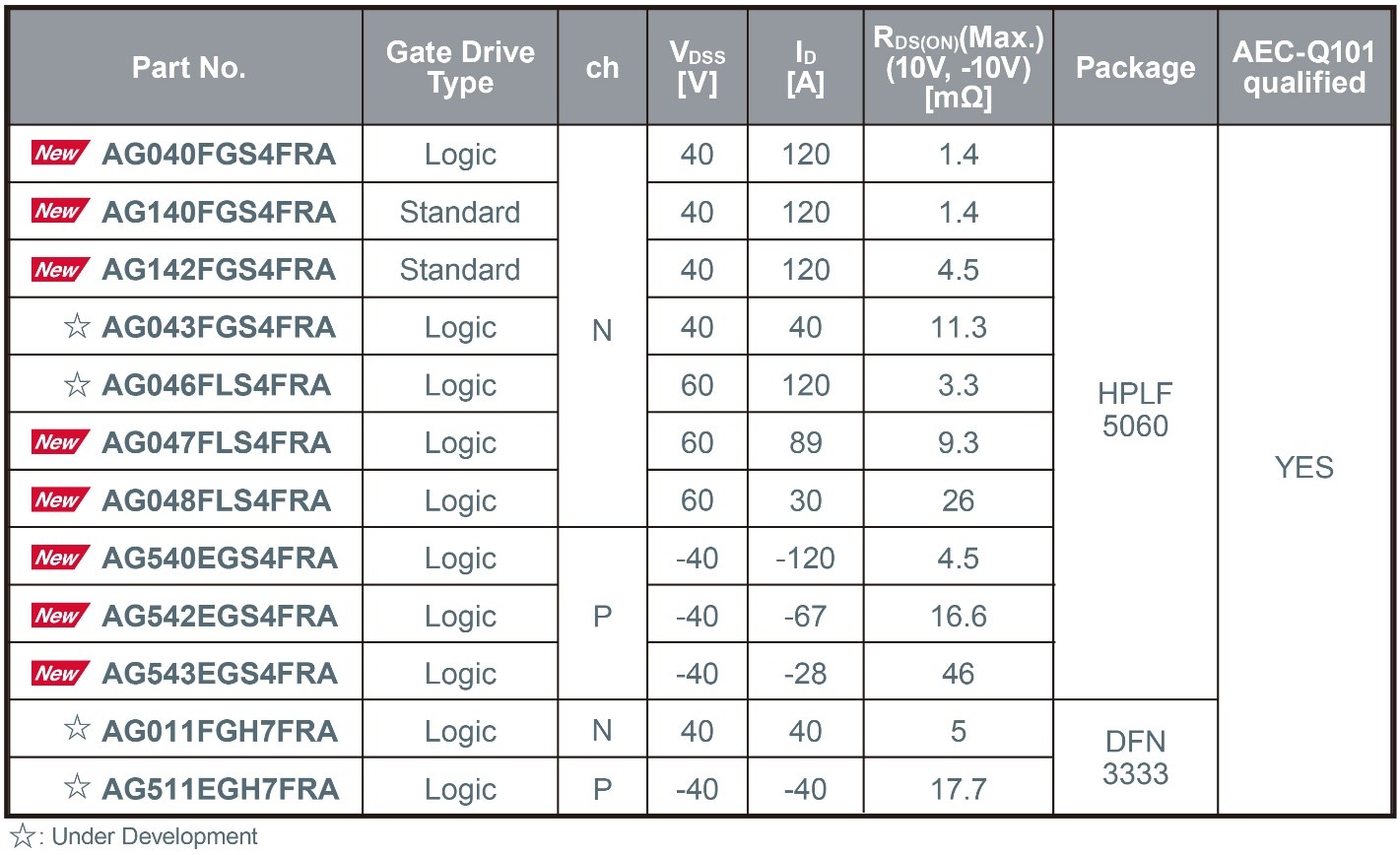
ROHM’s New Compact, Highly Reliable Package Added to Automotive 40V/60V MOSFET Lineup
ROHM has expanded its lineup of low-voltage (40V/60V) MOSFETs for automotive applications – such as main inverter control circuits, electric pumps, and LED headlights – by introducing the latest products adopting the new HPLF5060 package (4.9mm × 6.0mm).
In recent years, automotive low-voltage MOSFETs have been trending toward smaller packages, such as the 5060-size and even more compact options. However, this miniaturisation introduces significant challenges for achieving reliable mounting, primarily due to narrow terminal spacing and leadless designs.
To address these issues, the new HPLF5060 package offers a smaller footprint compared to the widely used TO-252 package (6.6mm × 10.0mm) while enhancing board-mount reliability through the adoption of gull-wing leads. Additionally, the use of copper clip junction technology enables high-current operation, making the HPLF5060 an ideal solution for demanding automotive environments.
Mass production of new products using this package began in November 2025 (sample price: $3.5/unit, excluding tax). Online sales have also started, and the products are also available for online purchase through online distributors such as DigiKey and Farnell.
In addition to expanding the lineup of products using this package, mass production of the smaller DFN3333 (3.3mm × 3.3mm) package, which employs wettable flank technology, is scheduled to begin around February 2026. Furthermore, development has commenced on a TOLG (TO-Leaded with Gull-wing) package (9.9mm × 11.7mm) to further expand the lineup of high-power, high-reliability packages.
The post ROHM’s New Compact, Highly Reliable Package Added to Automotive 40V/60V MOSFET Lineup appeared first on ELE Times.
Fraunhofer ISE achieves record efficiencies for tandem photovoltaic modules
Building I2C-PPS. Part 2 - Planning
 | Continuing from the idea published a couple of days before - Building a programmable DC-DC Power Supply with I2C Interface (I2C-PPS). Part 1 - Idea. I decided to get some intuition about overall device structure before gathering its schematics. As I sketched it in the picture the buck-boost converter can be seen as the set of several blocks - a power stage, input and output filters with respective current sensors, a set of programming resistors, a digital I/O plus indication circuit, and a master switch. The power stage consist of 4 power MOSFETs and the inductor. The input and output filters are sets of capacitors mixed with current sensing resistors. The converter's operation mode and HW limits on voltage and current are set by programming resistors. And digital I/O with indication circuit provides interface for RPI and some leds for us - humans. The master switch makes it possible to start or shutdown the thing as it needed independently by RPI as it's needed. Normally, it should stay off and should go off if RPI goes down turning the converter off when input voltage is here without running RPI. For the switcher TI provides a design calculator in form of an excel spreadsheet and schematic design checklist which allow to select values for main components with desired input and output specs in mind. As for now I decided to go with 4-6V input window but it really should stay at 5V and set HW input and output current limits at 5A. With 250kHz switching frequency many 10uH inductors with Isat > 7A and DCR in recommended range should work along with set of recommended power MOSFETs. More details you can find in the project repo - github.com/condevtion/i2c-pps. Looks like it's time to pull KiCAD into the project. [link] [comments] |
AI in 2026: Enabling smarter, more responsive systems at the edge

As artificial intelligence (AI) continues its momentum across the electronics ecosystem, 2026 is shaping up to be a defining year for edge AI. After years of rapid advancement in cloud‑centric AI training and inference, the industry is reaching a tipping point. High‑performance intelligence is increasingly migrating to the edge of networks and into systems that must operate under stringent constraints on latency, power, connectivity, and cost.
This shift is not incremental. It reflects a broader architectural evolution in how engineers design distributed intelligence into next‑generation products, systems, and infrastructure.
Consider an application such as detecting dangerous arc faults in high‑energy electrical switches, particularly in indoor circuit breakers used in residential, commercial, or industrial environments. The challenge in detecting potential arc faults quickly enough to trip a breaker and prevent a fire hazard is that traditional threshold‑based criteria often generate an impractically high number of false positives, especially in electrically noisy environments.
An AI‑based trigger‑detection approach can significantly reduce false positives while maintaining a low rate of false negatives, delivering a more practical and effective safety system that ultimately saves lives.
What edge AI means for design
Edge AI refers to artificial intelligence processing performed on or near the physical hardware that collects and acts on data, rather than relying solely on remote cloud data centers. By embedding inference closer to where data originates, designers unlock real‑time responsiveness, tighter privacy controls, and reduced dependence on continuous network connectivity.
These capabilities allow systems to make decisions in milliseconds rather than seconds, a requirement across many industrial and embedded domains.

Figure 1 Smart factory environments demand immediate pattern recognition and decision‑making.
From factory automation to safety‑critical monitoring, the need for immediate pattern recognition and decision‑making has become a core design constraint. Systems must be engineered to operate with local intelligence that is context‑aware and resilient, maintaining performance even during intermittent or unavailable cloud connectivity.
Engineering drivers behind the edge shift
Design engineers are responding to several overlapping trends.
- Latency and determinism
Latency remains a fundamental limiter in real‑time systems. When AI models execute at the edge instead of in the cloud, network round‑trip delays are eliminated. For applications such as command recognition, real‑time anomaly detection, and precision control loops, deterministic timing is no longer optional—it is a design requirement.

Figure 2 Latency issues are driving many industrial applications toward edge AI adoption.
In the arc‑fault detection example described earlier, both latency and determinism are clearly essential in a safety‑oriented system. However, similar constraints apply to other domains. Consider an audio‑based human‑machine interface for an assistive robot or a gesture‑based interface at an airport kiosk. If system response is delayed or inconsistent, the user experience quickly degrades. In such cases, local, on‑device inference is critical to product success.
- Power and energy constraints
Embedded platforms frequently operate under strict power and energy constraints. Delivering AI inference within a fixed energy envelope requires careful balancing of compute throughput, algorithm efficiency, and hardware selection. Engineering decisions must support sustained, efficient operation while staying within the electrical and packaging limits common in distributed systems.
- Data privacy and security
Processing AI locally reduces the volume of sensitive information transmitted across networks, addressing significant privacy and security concerns. For systems collecting personal, operational, or safety‑critical data, on‑device inference enables designers to minimize external exposure while still delivering actionable insights.
For example, an occupancy sensor capable of detecting and counting the number of people in hotel rooms, conference spaces, or restaurants could enable valuable operational analytics. However, even the possibility of compromised personal privacy could make such a solution unacceptable. A contained, on‑device system becomes essential to making the application viable.
- Resource efficiency and scalability
In deployments involving thousands or millions of endpoints, the cumulative cost of transmitting raw data to the cloud and performing centralized inference can be substantial. Edge AI mitigates this burden by filtering, transforming, and acting on data locally, transmitting only essential summaries or alerts to centralized systems.
Edge AI applications driving design innovation
Across industries, edge AI is moving beyond pilot programs into full production deployments that are reshaping traditional design workflows.
Industrial systems
Predictive maintenance and anomaly detection now occur directly at the machine, reducing unplanned downtime and enabling real‑time operational adjustments without dependence on remote analytics.

Figure 3 Edge AI facilitates predictive maintenance directly at the machine.
Automotive and transportation
In‑vehicle occupancy sensing is emerging as a critical edge AI application. Systems capable of detecting the presence of passengers—including children left in rear seats—must operate reliably and in real time without dependence on cloud connectivity.
On‑device AI enables continuous monitoring using vision, radar, or acoustic data while preserving privacy and ensuring deterministic system response. These designs prioritize safety, low power consumption, and secure local processing within the vehicle’s embedded architecture.
Consumer and IoT devices
Smart devices that interpret voice, gesture, and environmental context locally deliver seamless user experiences while preserving battery life and privacy.
Infrastructure and energy
Distributed assets in energy grids, utilities, and smart cities leverage local AI to balance loads, detect dangerous arc faults, and optimize performance without saturating communication networks. A common theme emerges across these sectors: the more immediate the required intelligence, the closer the AI must reside to the data source.
Design Considerations for 2026 and beyond
Embedding intelligence at the edge introduces new complexities. Beyond system design and deployment, AI development requires structured data collection and model training as both an initial and ongoing effort. Gathering sufficiently diverse and representative data for effective model training demands careful planning and iterative refinement—processes that differ from traditional embedded development workflows.
However, once structured data collection becomes part of the engineering lifecycle, many organizations find that it leads to more practical, cost‑effective, and impactful solutions.
Beyond data strategy, engineers must address tight memory footprints, heterogeneous compute architectures, and evolving toolchains that bridge model training with efficient, deployable inference implementations. A holistic approach requires profiling real‑world operating conditions, validating model behavior under constraint, and integrating AI workflows with existing embedded software and hardware stacks.
In this context, the selection of compute architecture and development ecosystem becomes critical. Platforms offering a broad performance range, robust security mechanisms, and long product lifecycles enable designers to balance immediate requirements with long‑term roadmap considerations. Integrated development flows that support optimization, profiling, and debugging across the edge continuum further accelerate time to market.
Edge AI in 2026 is not simply a buzz phrase—it’s a strategic design imperative for systems that must act quickly, operate reliably under constraint, and deliver differentiated performance without overburdening networks or centralized infrastructure.
By bringing intelligence closer to where data is generated, engineers are redefining what distributed systems can achieve and establishing a new baseline for responsive, efficient, and secure operation across industries.
Nilam Ruparelia is associate director of Microchip’s Edge AI business unit.
Special Section: AI Design
- The AI design world in 2026: What you need to know
- AI workloads demand smarter SoC interconnect design
- AI’s insatiable appetite for memory
- The AI-tuned DRAM solutions for edge AI workloads
- Designing edge AI for industrial applications
- Round pegs, square holes: Why GPGPUs are an architectural mismatch for modern LLMs
- Bridging the gap: Being an AI developer in a firmware world
- Why power delivery is becoming the limiting factor for AI
- Silicon coupled with open development platforms drives context-aware edge AI
- Designing energy-efficient AI chips: Why power must Be an early design consideration
- Edge AI in a DRAM shortage: Doing more with less
The post AI in 2026: Enabling smarter, more responsive systems at the edge appeared first on EDN.
The Rise of the AgentEngineer: How AI is Orchestrating the Future of Chip Design
While traditional Electronic Design Automation tools have been faithfully executing commands for decades, today’s agentic AI systems are rewriting the rulebook by thinking, iterating, and problem-solving autonomously across entire design workflows. Picture this: specialised AI agents functioning like a virtual design team—complete with their own CEO, CTO, and engineering specialists—orchestrating everything from RTL generation to physical design verification in feedback-driven loops that don’t just respond to errors, they anticipate and resolve them. This isn’t your standard chatbot-writes-some-code scenario; we’re talking about multi-agent architectures powered by Large Language Models that refuse to call it a day until every simulation passes. As the semiconductor industry grapples with a workforce crisis that threatens to bottleneck innovation, these AI systems are emerging as more than assistants; they’re becoming co-designers capable of exponentially multiplying engineering productivity. To understand how industry leaders are navigating this transformation from AI-assisted to AI-orchestrated design, we reached out to companies at the forefront of this revolution.
Architecture to Autonomy: Building Multi-Agent AI Systems for Chip Design
The semiconductor design floor is witnessing an unprecedented transformation where intelligent agents collaborate, critique, and refine work autonomously, like a seasoned design team operating at machine speed.
The Multi-Agent Architecture
Industry implementations structure these systems around specialised agent roles: RTL generation specialists handle code synthesis, verification agents scrutinise design correctness, and physical design agents optimise layouts. The orchestration framework manages task routing and dependencies, ensuring coherent workflow progression. Critically, these agents don’t replace existing EDA platforms; instead, they orchestrate them, invoking synthesis runs and analysing timing reports with minimal human intervention.
LLM Selection and Domain Adaptation
Behind these agents run Large Language Models serving as inference engines. The industry has split between proprietary models like GPT-4 and Claude, which offer robust reasoning capabilities, and open-source alternatives such as DeepSeek-Coder and Llama variants, providing customisation flexibility for high-volume workloads.
Raw LLMs produce generic code, but semiconductor design demands precision. Organisations implement two adaptation strategies: Retrieval-Augmented Generation (RAG) connects LLMs to design rule manuals, timing libraries, and verified IP repositories, grounding outputs in proven patterns. Domain-specific fine-tuning retrains models on millions of lines of verified RTL, enabling them to recognise design intent from terse specifications and suggest synthesis-aligned optimisations.
Talking about choosing the “right” LLM, 
Addressing Code Hallucination
The critical challenge remains code hallucination, plausible but incorrect outputs. Industry leaders deploy multi-layered validation: formal verification integration, simulation-in-the-loop refinement cycles, constraint-guided generation, and mandatory human review checkpoints for critical path logic. As one verification lead noted, AI-generated RTL receives the same scrutiny as junior engineer code, but iterates at 100x speed before human review.
“Hallucination is not a mysterious AI problem. It is the result of under-specified intent. We deal with it the same way we deal with junior engineers: through validation gates. Every AI-generated output passes through linting, simulation, coverage analysis, and equivalence checks. Nothing bypasses human review for critical design decisions. Trustworthy output comes from engineering discipline applied to AI, not from believing AI will magically become trustworthy,” added Gupta.
The technical architecture is maturing rapidly, but the true test ahead is scaling from engineer assistance to autonomous subsystem design, determining whether agentic AI becomes indispensable infrastructure or remains an expensive experiment.
AgentEngineer Revolution: Transforming Roles and Multiplying Productivity
The automation wave reshaping semiconductor design isn’t just changing workflows—it’s fundamentally redefining what it means to be a design engineer in 2026.
Quantifiable Productivity GainsEarly adopters report transformative productivity metrics. RTL generation rates have surged from approximately 50-100 lines per engineer-day in manual workflows to 500-1,000+ lines with AI assistance—a 10x improvement when measured by functional complexity rather than raw line count. Time-to-tapeout reductions range from 20-40% for complex SoC projects, with verification cycles seeing the most dramatic compression.
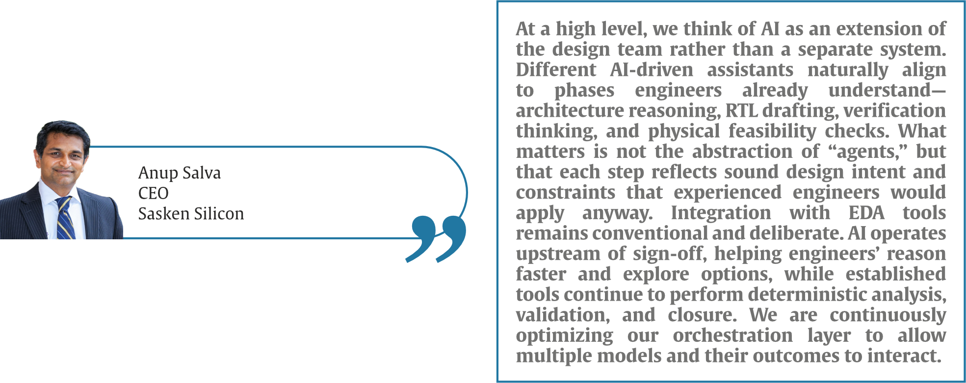
“The biggest gains have come from reducing friction, not replacing engineers. Tasks that previously required multiple iteration initial RTL structure, verification scaffolding, and early debug hypotheses now converge faster. We typically see meaningful schedule compression in early and mid-design phases, allowing teams to spend more time on optimisation, corner cases, and RF-digital interactions. This has increased our capacity to take on more complex mixed-signal and SoC programs without sacrificing rigour,” explains Anup Salva, CEO, Sasken Silicon.
Verification coverage metrics tell an equally compelling story. AI-driven testbench generation achieves 85-95% functional coverage in initial passes compared to 60-70% with manual approaches, while bug detection rates during pre-silicon validation have improved by 30-50%. One design team reported identifying critical corner-case failures that traditional directed tests missed entirely, caught by AI agents exploring unconventional stimulus patterns.
Perhaps most significant: engineering teams report handling 2-3x more concurrent design projects without proportional headcount increases, effectively multiplying organisational capacity during an industry-wide talent shortage.
The Evolving Engineer RoleThe shift from manual RTL coding to AI-orchestrated design is forcing a fundamental role transformation. Traditional design engineers spent 60-70% of their time writing and debugging code. Today’s “AgentEngineers” allocate that time differently: 40% on high-level architectural specification and constraint definition, 30% on AI output validation and refinement, 20% on system integration and optimisation, and just 10% on direct coding for critical path logic AI cannot yet handle reliably.
Talking on the evolving role of Engineers in the AI era, Srinivas Gupta, CEO, Silicon Patterns, emphasises that, “AI is not eliminating engineering roles, it is exposing who is adding real value. The role of the engineer is shifting from manual construction to intent definition, supervision, and judgment. Writing RTL is no longer the bottleneck; understanding what should be written and why is. Effective training is not about teaching “prompt engineering.” It is about teaching engineers how to reason clearly, review outputs critically, and understand failure modes. The best learning happens when AI is embedded directly into real project workflows, spec reviews, verification bring-up, debug, not in isolation.”
New competencies are emerging as essential: prompt engineering skills to communicate design intent effectively to LLM agents, AI system supervision capabilities to recognize when autonomous agents are diverging from design goals, and elevated architectural thinking to work at higher abstraction layers. The most successful engineers are those who transition from implementation experts to design orchestrators—defining what to build while delegating how to build it.
Training for TransformationOrganisations are implementing structured transition programs. Technical training covers AI model capabilities and limitations, effective prompt crafting for design specifications, and verification strategies for AI-generated code. Just as importantly, cultural training addresses the psychological shift from individual contributor to AI collaborator, teaching engineers when to trust autonomous outputs and when human judgment remains irreplaceable.
The semiconductor workforce crisis that threatened industry growth is being addressed not through massive hiring campaigns, but through radical productivity multiplication—a smaller cohort of AgentEngineers accomplishing what previously required entire design teams.
Trust, Validation, and the Road to 2026: Overcoming Deployment Challenges
Agentic AI’s technical promise confronts harsh deployment realities. The path from laboratory demonstration to production tapeout demands solving trust, integration, and scalability challenges that determine whether this technology revolutionises the industry or remains confined to pilot projects.
The Three Critical Deployment ChallengesIntegration Complexity tops the challenge list. Legacy EDA environments weren’t architected for AI orchestration—tool licenses limit concurrent sessions, APIs lack programmatic access depth, and design databases struggle with AI agents’ iterative read/write intensity. Organisations report 6-12 month integration timelines just to achieve basic agent-tool interoperability.
Trust and Validation Frameworks represent the existential challenge. For tape-out critical stages—final timing closure, DFT insertion, physical verification—engineers demand confidence levels AI systems cannot yet guarantee. One design director noted, “We can’t ship silicon that passes simulation but fails in production because an AI agent hallucinated a clock domain crossing fix.”
Organisational Resistance manifests subtly but persistently. Experienced engineers trained over decades resist delegating design authority to probabilistic systems. Version control becomes contentious when distinguishing human versus AI contributions. Accountability questions arise when AI-generated blocks cause post-silicon failures.
Building Trust Through ValidationSuccessful deployments implement rigorous validation hierarchies. AI-generated RTL undergoes formal equivalence checking against specifications, simulation coverage thresholds exceed 95% before human review, and critical paths receive mandatory expert sign-off regardless of AI confidence scores. Human-in-the-loop checkpoints gate progression, with engineers retaining veto authority at every stage.
Observability tools provide transparency into AI decision-making—logging which training examples influenced specific design choices, tracking confidence metrics for generated code segments, and flagging low-confidence outputs for immediate human review.
The 2026 Automation RoadmapIndustry consensus positions current systems at Level 2 on the five-level autonomy scale: capable assistants requiring continuous supervision. Reaching Level 4—autonomous subsystem design with minimal oversight—demands breakthroughs across multiple fronts.
Enhanced LLM reasoning must progress beyond pattern matching to genuine architectural trade-off analysis, understanding power-performance-area implications of micro-architectural choices. Memory systems need expansion to manage entire SoC contexts rather than isolated module designs. Formal methods integration must advance from post-generation validation to constraint-guided generation, preventing invalid designs rather than detecting them.
On the India front, Anup Salva, CEO, Sasken Silicon, notes that, “India’s advantage lies in its depth of engineering intuition, especially in areas like RF, analogue, and system-level integration. These are domains where AI works best as a multiplier, not a replacement. Over the next few years, we expect higher automation in well-understood design spaces, but always guided by engineers who understand the underlying physics and architecture. Progress will be driven more by better problem formulation and design discipline than by radical new tools.”
The competitive landscape trajectory appears clear: by late 2026, agentic AI will likely transition from a competitive differentiator to table stakes. Organisations not deploying these systems risk falling behind on time-to-market metrics. Yet the dominant paradigm will remain hybrid human-AI workflows rather than full autonomy—engineers orchestrating AI agents rather than being replaced by them, at least through this decade.
by: Shreya Bansal, Sub-Editor
The post The Rise of the AgentEngineer: How AI is Orchestrating the Future of Chip Design appeared first on ELE Times.
I love my teacher
 | submitted by /u/RequiemOfLigh [link] [comments] |
USB Hub made entirely of TH components
 | Didnt think it was a thing! Would have expected some mandatory SMT ICs [link] [comments] |
Wolfspeed adds VP of sales for EMEA
Passive RC circuit produces gain

Could a simple passive RC network without any transformers, inductors, switches, or non-linear components produce a voltage gain?
Wow the engineering world with your unique design: Design Ideas Submission Guide
Well, it’s not “free energy,” however, yes, and can even use the same value resistor and capacitor in a ladder network shown in Figure 1, although differing values also can be utilized.
 Figure 1 Passive RC circuit using resistors and capacitors of the same value in a ladder network.
Of course, this isn’t of much use other than a curiosity, but it’s a fun circuit to build and play around with!
I built one with seven sections (Figure 2) using an R of 10 kΩ and a C of 0.1 µF, then plotted the results.

Figure 2 A seven-section RC ladder network with an R of 10 kΩ and C of 0.1 µF.
The Bode plot can be seen in Figure 3. As you can see, the gain remains around 0 dBv and behaves as a low-pass filter, then slowly rises to a peak of 1.07 dBv at 1 kHz before falling off.

Figure 3 Bode plot of the passive RC circuit showing low-pass filter behavior until a slow rise to a peak of 1.07 dBv at 1 kHz.
This agrees well with the simulation shown in Figure 4.

Figure 4 Circuit simulation of a passive RC circuit that closely matches the Bode plot shown in Figure 3.
If you swap the resistors and capacitors, the circuit behaves like a high-pass filter and produces a higher gain of 1.13 dBv at 26 Hz, as shown in Figure 5, and a simulation in Figure 6.

Figure 5 Bode plot of the passive RC circuit showing high-pass filter behavior.

Figure 6 Circuit simulation of a passive RC circuit that closely matches the Bode plot shown in Figure 5.
As noted by someone, this technique can be employed with an emitter-follower, which has a voltage gain less than unity to create an oscillator. However, that’s for another upcoming Design Idea (DI), which will also include a note on how a single unbiased JFET can produce a +dBv voltage gain!
Anyway, hopefully some folks find this interesting and have some fun!
Michael A Wyatt is a life member with IEEE and has continued to enjoy electronics ever since his childhood. Mike has a long career spanning Honeywell, Northrop Grumman, Insyte/ITT/Exelis/Harris, ViaSat, and retiring (semi) with Wyatt Labs. During his career, he accumulated 32 US Patents and, in the past, published a few EDN Articles, including Best Idea of the Year in 1989.
Related Content
- RC networks
- SPICE Course, Part 2: Time Constant Simulation
- Designing RC active filters with standard-component values
- A simple software lowpass filter suits embedded-system applications
The post Passive RC circuit produces gain appeared first on EDN.
Tower and Scintil announce availability of first heterogeneously integrated DWDM lasers for AI infrastructure
Build a practical 400 mA linear Li-ion charger with visible CC-CV behavior

Single-cell lithium-ion (Li-ion) chargers are widely used, yet many practical designs rely on highly integrated ICs that conceal their internal operation. The type of Li-ion charger outlined in this design is, somewhat surprisingly, not readily found in a general review of available internet and YouTube resources.
Wow the engineering world with your unique design: Design Ideas Submission Guide
The present circuit is practical, deployable, and firmly grounded in established circuit theory, and may offer a complementary perspective to prevailing practice, particularly for designers who value analytical transparency and first-principles reasoning. It operates from a 5 V supply, commonly found in 5 V/1 A smartphone chargers, delivers 400 mA of constant current (CC), then transitions to 4.217 V constant-voltage (CV) regulation, and has been built and tested using half of an LM324 quad operational amplifier.
The circuit, shown in Figure 1, performs reliably and is well-suited for bench chargers, embedded products, and instructional laboratories. This design emphasizes simplicity, component availability, and safe charging behavior while remaining easy to analyze and adapt.

Figure 1 Schematic of the dual-loop linear Li ion charger. The schematic shows the key nodes that are referenced and plotted in the LTSpice simulation. In practice, a 1N4007 diode for D2 also worked well.
The charger uses two independent control loops acting on a PNP pass transistor. An inner loop regulates charge current, while an outer loop regulates battery voltage. The voltage loop output also provides a convenient indicator of charging status.
CC loop operationA 1.25 V reference is divided using 115 kΩ and 10 kΩ resistors to produce a 0.10 V current reference. An LM324 section compares the 1.25 V reference to the drop across a 0.25 Ω sense resistor in series with the battery return. The op amp drives an NPN transistor, which sinks base current from the PNP pass device until the sense voltage equals the reference.
The resulting charge current is 0.4 A. This current regulation is independent of battery voltage, ensuring safe charging even from deeply discharged cells.
CV loop operationA second LM324 section monitors battery voltage through a 47.5 kΩ and 20 kΩ divider. When the divided voltage reaches 1.25 V, corresponding to 4.217 V at the battery terminals, the op amp reduces drive to the pass transistor, transitioning the charger into CV mode.
The voltage loop is intentionally compensated to be slower than the current loop, ensuring a smooth handover without oscillation or overshoot. As in my case, if a commercial 1.25-V reference, e.g., TLV431, is not available, a 2k/2k potential divider connected to the common LM431-2.5-V voltage reference works reasonably well. However, since it is an integral part of both control loops, extra care should be taken to stabilize the loops to prevent oscillations.
Loop stabilityThe changeover from CC to CV crossover can cause some ringing, as shown in the measurement of U2OUT shown in the DSO capture in Figure 2. This appears as both LEDs are dimly lit, showing rapid oscillations. There are two possible remedies. The first is to dampen the voltage loop by including a small capacitance of 33 pF to 500 pF in parallel with Rtop. The second is to dampen the current loop by adding a small RC time constant from the emitter to the collector of Q2, the pass transistor driver. In LTSpice, you can probe phase margin by injecting a small AC source at the summing point or by param sweeping and observing step responses.

Figure 2 Circuit construction and measurements. Inset (a) close-up of the breadboarded circuit showing the status indication LEDs. The photograph was taken when the cell voltage was 4.09 V, which is the threshold of the CC-CV crossover (see text). (b) shows the oscillation at the node U2OUT, which drives the LEDs and forms the pass transistor pre-driver signal. The image was captured on a Tektronix TDS2024C DSO.
Charge status indicationThe output of the voltage regulating amplifier doubles as a logic-level indicator of charging state. When the battery voltage is below the regulation threshold, the output drives a red LED indicating active charging. As the battery approaches full charge and current tapers, the output level changes and illuminates a green LED. This approach eliminates the need for an additional comparator while providing clear, real-time visual feedback.
Thermal and practical considerationsWith a deeply discharged cell at approximately 2.2 V, the PNP pass transistor must dissipate roughly 1.1 W at 400 mA. Off-the-shelf, low saturation voltage transistors such as the 2SB772 will work comfortably without a heat sink. In the constructed prototype, a modest copper area was sufficient for thermal management. Although in the built version a 5W rating is used for the sense resistor, it dissipates only 40 mW, allowing a 0.25 W rated component a more than adequate margin. All active components operate within their safe operating area when supplied from a regulated 5 V source.
Experimental verificationThe charger was assembled on a prototype board and tested with a single 18650 Li-ion cell. Startup into CC mode was immediate, followed by a smooth transition to CV operation at approximately 4.22 V. Charge current tapered naturally as expected.
Supplementary files:
- A video of the circuit in operation is shown here: https://youtube.com/shorts/oSzR4XQViFs
- LTSpice simulation (.asc) file: Li-ion-ocaya-LTSpice schematic.asc
The LTspice simulation models the Li-ion cell as an ideal capacitor C in series with a small ESR = 80 mΩ, charged from a constant current I = 0.4 A source; the terminal voltage is
![]() where the capacitive core obeys:
where the capacitive core obeys:
![]()
Over a finite interval ΔV and time Δt, the approximation C = I Δt/ΔV can be made, assuming that the current is reasonably constant. The current falls progressively in reality, imparting a non-linear character to the cell voltage transient. With the cell rising from 2.2 V to 4.217 V, the ESR contributes a small, essentially instantaneous step of = 0.4 × 0.08 = 0.032 V (32 mV), after which the slope is set by I/C. Thus, if the observed CC interval Δt for the ΔV ≈ (4.217 − 2.2) = 2.017 V rise is about 5250 s (≈ 1.46 h), then C ≈ (0.4 × 5250) / 2.017 ≈ 1040 F.
This is a first-order capacitor-plus-ESR approximation, with the caveat that real Li-ion cells have voltage–state-of-charge (SoC) and temperature dependencies that make C a state-dependent quantity rather than a fixed constant.
Figure 3 plots the LTSpice simulation values of the nodes and branches named in Figure 1. In Figure 3, the battery was assumed to be deeply discharged, denoted by a state of charge of 2.2 V.

Figure 3 LTspice simulation of the key nodes and currents in the circuit. The measurements on the actual circuit closely match these plots.
The simulation shows that it transited from CC to CV charging in approximately 1 hr 21 mins after the onset of charging. The charging current tapered off thereafter and dropped to zero. The circuit current dropped to 19 mA without the battery connected, and when the charging was completed. The measured voltage across the Li-ion was 4.21 V, with only the green LED fully on, with no flickering on either LED, as shown in Figure 4.

Figure 4 Photographs showing the current drawn by the circuit from a 5-V bench supply, and a multimeter showing a 4.21 V SoC of the Li-ion battery when charging is completed.
Compliant Li-ion chargingThis design demonstrates that a fully compliant Li-ion charging profile can be achieved using readily available analog components. It is suitable for real-world use while remaining accessible to analysis and modification. The circuit offers a practical alternative for engineers who require simplicity, transparency, and predictability in low-power Li-ion charging applications.
P.S.: Like many enthusiasts around the world, the designer lives in a region where access to electronics stores and new components is limited. The motivation for this circuit was robustness and realizability using parts salvaged from discarded equipment.
Professor Ocaya specializes in electronics and solid-state physics, which he teaches at the Qwaqwa Campus of the UFS. He is active in computing, mathematical methods, new techniques for device characterization, material science, and microcontroller-based instrument design. He holds a C3 rating from the National Research Foundation (NRF) of South Africa.
Related Content
- Circuit’s RMS output is linearly proportional to temperature over wide range
- A battery charger that does even more
- Building a Battery Charger with the CC/CV Method
- Lead-acid battery charger
The post Build a practical 400 mA linear Li-ion charger with visible CC-CV behavior appeared first on EDN.
IIIT Hyderabad’s Smart Approach To Sand Mining Enforcement, Incorporating AI in Trucks
‘Truck art’ or the hand-painted ‘Horn Ok Please’, ‘Use Dipper at Night’ and the ‘Buri nazar waale tera mooh kala’ are an integral part of Indian highways. These artistic expressions, which lighten up many a road journey, also find an extension in hand-painted registration plates. However, such unstandardised lettering can prove to be a challenge for automatic number plate recognition (ANPR) systems. Most commercial ANPR systems are designed for standardised license plates. ANPR systems play a crucial role in modern governance, helping authorities monitor traffic, enforce regulations, prevent illegal transport, and improve public safety. From toll booths to traffic violations, ANPR enables real-time vehicle tracking without manual checks.
A Unique Number Plate Problem
Hence, when the Telangana IT Department approached IIIT-H, seeking an ANPR solution for the Telangana Mineral Development Corporation (TGMDC), their requirement was very different from typical commercial use cases.TGMDC was on the lookout for a cost-effective, robust solution tailored to monitor sand mining trucks, primarily to curb illegal mining and transport. “Typical license plates are actually easy to detect,” explains Dr. Veera Ganesh Yalla, CEO of iHub-Data and Adjunct Faculty at IIIT-H. But in India, especially with trucks, plates are often hand-painted, inconsistent, and highly variable. “They might follow black lettering on a yellow background, but from vehicle to vehicle, their design, the style, everything is unique,” he says, making off-the-shelf solutions for their detection both ineffective and expensive.

Building Smart, Not From Scratch
Commercial systems are typically very expensive, with per-camera costs of licensing and maintenance running into tens of lakhs. Leveraging prior research from Prof. Ravikiran Sarvadevabhatla’s team at the Centre for Visual Information Technology, IIIT-H, where a prototype license plate recognition system had been developed, the iHub-Data team took the research forward into real-world deployment. “The lab tech was more like a research prototype, not really for scaling or translation. So we decided to take it and see what we could do,” Dr. Yalla recalls. The team studied the workflow, rebuilt and strengthened the handwritten character recognition component. What’s unique is that they integrated the analytics as a plug-in into an open-source platform. ”If anybody wants to plug in our license plate technology into their platform, they can do it without having to rewrite their entire platform from scratch,” he notes.
Real-life Deployment
Their solution, named Vahan Eye, was piloted at Chityal on the Vijayawada–Hyderabad highway, where the team installed cameras, laid cables, and deployed the system end-to-end. The deployment tracks trucks entering Telangana and cross-checks them against a whitelist of nearly 40,000 approved vehicles. Tweaked specially to suit the needs of TGMDC, the solution offers customised dashboards. Since September, the system has been running continuously. Despite challenges such as low lighting at night and festival-related obstructions such as garlands covering the number plates, the algorithm has proven robust and continues to improve with live data.

From PoC to Public Impact
Built by a lean team of fewer than five engineers and powered by modern deep learning models, Vahan Eye demonstrates how lab research can be translated into an affordable, field-ready public solution. “Our IP is that we really figured out how to solve this whole handwritten license plate character problem,” says Dr. Yalla. Currently, the team is working on customising the solution for the Police Department for automatic detection of traffic violations by 2-wheelers.
Dr. Yalla, who began his career in the video surveillance industry with classical machine learning solutions that used support vector machines, explains that with advances in deep learning, more powerful algorithms such as YOLO and RF-Detr are now being applied, leading to significantly improved performance and accuracy. As he puts it, the goal is clear: prove the technology works, make it accessible at a fraction of commercial costs, and enable scalable adoption across government departments.
The post IIIT Hyderabad’s Smart Approach To Sand Mining Enforcement, Incorporating AI in Trucks appeared first on ELE Times.
Applied Materials, CG Power, Lam Research, Larsen & Toubro, and Micron Join the IDTA
The India Deep Tech Alliance (IDTA) announced that Applied Materials, CG Power, Lam Research, Larsen & Toubro, and Micron Technology have joined the Alliance. These additions further strengthen IDTA’s cross-sector collaboration model, which brings together investors, corporates, and technology-enabling partners to mobilise capital, technical expertise, market access, and policy engagement for the advancement of Indian deep tech startups.
With the addition of these global and Indian industry leaders, IDTA now spans artificial intelligence, semiconductor equipment, memory, materials, infrastructure engineering, and power systems, creating an integrated platform to support investment, technology collaboration, talent development, and startup commercialisation. With the shared goal of accelerating the growth of India’s deep tech economy, IDTA Corporate Strategic Partners aim to leverage their expertise to provide strategic and technology counsel to other IDTA members and emerging startups. Strategic advisory and ecosystem collaborations may include:
- Manufacturing and scale-up guidance for lab-to-fab transitions and production readiness.
- Technical talks, training, and access to expert resources.
- Collaborative research discussions and ecosystem initiatives with startups, researchers, and industry.
- Private industry input to policy dialogues related to national priority technology sectors.
- Mentorship, network access, and co-development opportunities in concert with investors.
IDTA is an industry-led consortium formed to mobilise capital and company-building expertise to help India-domiciled deep tech startups scale globally. It was formed to expand private sector support for strategic technology sectors, complementing the Government of India’s Research, Development & Innovation (RDI) Scheme.
This latest membership expansion follows NVIDIA joining IDTA as a Founding Member and Strategic & Technical Advisor, underscoring the Alliance’s ambition to build globally relevant, India-anchored deep tech capabilities at scale. Since its founding in September 2025, IDTA has expanded to a commitment of more than $2.5B USD in venture funding to Indian deep tech startups over the next five years, including a dedicated $1B USD allocation to Indian AI startups to be invested over the next three years. IDTA venture capital members have deployed $110M USD into 50+ companies over the past six months.
“The entry of Applied Materials, CG Power, Lam Research, L&T, and Micron marks a pivotal step in moving India’s deep tech ambition from intent to execution,” said Arun Kumar, India Managing Partner of Celesta Capital and Chair of IDTA. “Together with NVIDIA’s role as a founding member and strategic advisor, this coalition brings unmatched depth across semiconductors, advanced manufacturing, infrastructure, and systems engineering. IDTA is designed to align capital, technology, and policy so that India can emerge not just as a participant, but as a trusted global hub for next-generation technologies.”
Quotes from New IDTA Corporate Strategic Partners:
Om Nalamasu, CTO, Applied Materials, said, “Applied Materials has a long history of working across industry, startups, academia, and research institutions to advance foundational technologies. As a materials engineering leader, we believe long‑term progress comes from sustained, ecosystem‑level collaboration. Through this alliance, we look forward to contributing our deep technology expertise to help build resilient ecosystems for India and the world.’’
Mr. Amar Kaul, Global CEO & Managing Director, CG Power, said, “India’s deep tech journey is entering a decisive phase, one where execution, industrial capability, and long-term partnerships will determine global relevance. CG Power’s participation in the India Deep Tech Alliance reflects our conviction that nation-building today requires strong, technology-led manufacturing ecosystems. Through IDTA, we look forward to contributing our expertise in industrial, power systems and semiconductors to create resilient and future-ready value chains that reinforce India’s position as a trusted global technology hub.”
Kevin Chen, Head of Lam Capital & Corporate Development, Lam Research, said: “Semiconductor manufacturing excellence depends on deep collaboration across equipment, materials, process technology, and talent. We look forward to engaging with IDTA to help Indian innovators navigate technology roadmaps, manufacturability, and global ecosystem linkages that accelerate from lab to fab.”
Prashant Chiranjive Jain, Head Corporate Centre, Larsen & Toubro, said: “The India Deep Tech Alliance represents a pivotal shift toward indigenous innovation. By synergising L&T’s engineering heritage with advanced capabilities in AI, design engineering, and quantum systems, we are committed to building a robust deep-tech ecosystem. We look forward to delivering cutting-edge solutions that position India as a global leader in the next generation of technology.”
Anand Ramamoorthy, Managing Director, Micron India, said: “Micron’s decision to join the India Deep Tech Alliance reflects our commitment to ecosystem-led collaboration to propel a vital economic engine for India. Micron’s technology and innovation expertise will play a vital role in helping advance globally competitive deep tech from India while aligning with IDTA’s support for the national RDI agenda and its focus on translating research into market impact.”
The post Applied Materials, CG Power, Lam Research, Larsen & Toubro, and Micron Join the IDTA appeared first on ELE Times.
Звіт проректора з наукової роботи КПІ Сергія Стіренка на засіданні Вченої ради 12 січня 2026 року: "Науково-інноваційна діяльність університету як складова сталого зростання"

Шановні колеги, вашій увазі пропонується інформація про результати науково-інноваційної діяльності університету як складової сталого зростання за 2025 рік та про перспективи розвитку на рік 2026.
I made a digital clock with DIY etched PCB
 | I also wrote about it here https://boxart.lt/en/blog/diy_digital_clock [link] [comments] |
Сторінки


![[link]](https://i.redd.it/v9veatvgs7kg1.png)
![[link]](https://i.redd.it/obio4jbi06kg1.jpeg)
![[link]](https://i.redd.it/4z6i7vs104kg1.jpeg)