
At the recent Conformance Agreement Group (CAG) meeting #78 of the Global Certification Forum (GCF), Rohde & Schwarz verified NTN NB-IoT test cases for radio frequency (RF) and radio resource management (RRM), successfully meeting all test platform approval criteria (TPAC). The R&S TS-RRM and R&S TS8980 test platforms were approved for every type of NTN NB-IoT test (RF, Demod and RRM), making Rohde & Schwarz the only company to have activated both NTN NB-IoT radio frequency (RF) and radio resource management (RRM) work items (WI) in the GCF.
Новини світу мікро- та наноелектроніки
Power Tips #129: Driving high voltage silicon FETs in 1000-V flybacks

The 800 V automotive systems enable higher performance electric vehicles capable of driving ranges longer than 400 miles on a single charge and charging times as fast as 20 minutes. 800 V batteries rarely operate at exactly 800 V and can go as high as 900 V with converter input requirements up to 1000 V.
There are a number of power design challenges for 1000-V-type applications, including field-effect transistors (FET) selection and the need to have a strong enough gate drive for >1,000 V silicon FETs which generally have larger gate capacitances than silicon carbide (SiC) FETs. SiC FETs have the advantage of lower total gate charge than silicon FETs with similar parameters; however, SiC often comes with increased cost.
You’ll find silicon FETs used in designs such as the Texas Instruments (TI) 350 V to 1,000 V DC Input, 56 W Flyback Isolated Power Supply Reference Design, which cascodes two 950 V FETs in a 54 W primary-side regulated (PSR) flyback. In lower-power general-purpose bias supplies (<10 W), it is possible to use a single 1,200 V silicon FET in TI’s Triple Output 10W PSR Flyback Reference Design which is the focus of this power tip.
This reference design can be a bias supply for the isolated gate drivers of traction inverters. It includes a wide input (60 V to 1000 V) PSR flyback with three isolated 33 V outputs, 100 mA loads, and uses TI’s UCC28730-Q1 as the controller. Figure 1 shows the UCC28730-Q1 datasheet with a 20-mA minimum drive current.

Figure 1 Gate-drive capability of the UCC28730-Q1 with a 20-mA minimum drive current. Source: Texas Instruments
The challenge is that the 1,200 V silicon FET will have a very large input capacitance (Ciss) of around 1,400 pF at 100 V VDS, which is 4 times more than a similarly rated SiC FET.
With a relatively weak gate drive from the UCC28730-Q1, Equation 1 estimates the primary FET turn-on time to be approximately 840 ns.
![]()
Figure 2 shows that as FET gate-to-source capacitance (CGS) and gate-to-drain capacitance (CGD) increases, it consumes the on-time of the primary FET required to regulate the output voltage of the converter.

Figure 2 FET turn on and off curves, as FET CGS and CGD increase, it consumes the on-time of the primary FET required to regulate the output voltage of the converter. Source: Texas Instruments
Figure 3 shows the undesirable effect of this by looking at the gate voltage of the UCC28730-Q1 driving the primary FET directly. In this example, it takes approximately 800 ns to completely turn on the FET and 1.5 µs for the gate to reach its nominal voltage. As you go to 400 V, the controller is still trying to charge CGD when the controller decides to turn off the FET. It is much worse at 1,000 V where the CGS is still being charged before turning off. This shows that as the input voltage increases, the controller cannot output a complete on-pulse and therefore the converter cannot power up to nominal output voltage.

Figure 3 Gate voltage of UCC28730-Q1 directly driving the primary FET with increasing input voltage. Source: Texas Instruments
To solve this, you can use a simple buffer circuit using two low-cost bipolar junction transistors as shown in Figure 4.

Figure 4 Simple N-Channel P-Channel N Channel-, P-Channel N-Channel P-Channel (NPN-PNP) emitter follower gate-drive circuit. Source: Texas Instruments
Figure 5 shows the gate current waveform of the primary FET and demonstrates the buffer circuit capable of gate drive currents greater than 500 mA.

Figure 5 Gate drive buffer current waveform of PMP23431, demonstrating that the buffer circuit is capable of gate drive current greater than 500 mA. Source: Texas Instruments
As shown in Equation 2, this reduces the charge time to 33 ns and is 25 times faster compared to just using the gate drive of the controller.

A PSR flyback architecture typically requires a minimum load current to stay within regulation. This helps increase the on-time and the converter can now power up to its minimum load requirements at 1000 V as shown in Figure 6. The converter’s overall performance is in the PMP23431 test report and Figure 7 shows the switching waveform with constant pulses on the primary FET. At 1,000 V with the minimum load requirement, the on-time is approximately 1 µs. Without this buffer circuit, the converter would not power up to 1,000 V input.

Figure 6 Converter startup with minimum load requirement with a 1000-V input. Source: Texas Instruments

Figure 7 Primary FET switching waveform of PMP23431 at 1000 V input. Source: Texas Instruments
In high voltage applications up to 1,000 V, the duty cycle can be quite small—in the hundreds of nanoseconds. A high-voltage silicon FET can be the limiting factor to achieving a well-regulated output due to its high gate capacitances. This power tip introduced PMP23431 and a simple buffer circuit to quickly charge the gate capacitances to support the lower on-times of these high voltage systems.
 Darwin Fernandez is a systems manager in the Automotive Power Design Services team at Texas Instruments. He has been at TI for 14 years and has previously supported several power product lines as an applications engineer designing buck, flyback, and active clamp forward converters. He has a BSEE and MSEE from California Polytechnic State University, San Luis Obispo.
Related Content
- Power Tips #128: Designing a high voltage DC-link capacitor active precharge circuit
- Power Tips #76: Flyback converter design considerations
- Power Tips #98: Designing a DCM flyback converter
- Why use a BJT in a flyback converter?
- Power Tips #91: How to improve flyback efficiency with a nondissipative clamp
- Power Tips #77: Designing a CCM flyback converter
- Power Tips #17: Snubbing the flyback converter
Additional Resources
- Read the application note, “Practical Considerations in High-Performance MOSFET, IGPT and MCT Gate-Drive Circuits.”
- Check out the application report, “Fundamentals of MOSFET and IGBT Gate Driver Circuits.”
- Download the PMP41009 reference design.
googletag.cmd.push(function() { googletag.display('div-gpt-ad-native'); });
-->
The post Power Tips #129: Driving high voltage silicon FETs in 1000-V flybacks appeared first on EDN.
Categories: Новини світу мікро- та наноелектроніки
ESSCI Partners with IIT Guwahati & IIT Ropar to Boost Semiconductor Skill Development and Innovation
New Delhi: Electronics Sector Skills Council of India (ESSCI) proudly unveils a momentous leap forward in its relentless pursuit of skill development and innovation within the semiconductor domain. In a historic move, ESSCI has inked a game-changing Memorandum of Understanding (MoU) with the esteemed Indian Institutes of Technology (IIT) Guwahati and Ropar. This visionary collaboration is poised to ignite a revolution, fostering a dynamic ecosystem primed for skill enhancement, innovation acceleration, and the flourishing of semiconductor startups.
This MoU aims to train not only students from Indian Institutes of Technology (IITs) but also aspiring engineers from diverse academic backgrounds in various job roles crucial for the semiconductor industry. It will play a crucial role in providing skilled manpower to the industry, including Tata Semiconductor Assembly and Test Pvt Ltd (“TSAT”), which is in the process of establishing a semiconductor unit in Morigaon, Assam. This state-of-the-art facility, with a remarkable capacity of producing 48 million chips per day, is being constructed at an investment of Rs 27,000 crore. The facility will cater to diverse segments such as automotive, electric vehicles, consumer electronics, telecom, and mobile phones.
At the heart of this groundbreaking partnership lies the establishment of cutting-edge, industry-led skill centers dedicated to nurturing skilled manpower in semiconductor technology development and testing realms. This initiative includes Training of Trainers (ToT) programs under the National Skills Qualifications Framework (NSQF) standards, as well as the development of courses and programs aligned with industry standards.
Formalized amidst great anticipation in Guwahati, the MoU bears the signatures of luminaries Dr. Abhilasha Gaur, the dynamic Chief Operating Officer of ESSCI, and the venerable Prof. Rajeev Ahuja, serving as Director at both IIT Guwahati and IIT Ropar.
The momentum surged further as Dr. Abhilasha Gaur took the stage as a distinguished speaker at the prestigious Semiconductor Horizons Workshop hosted by IIT Guwahati. Her illuminating insights illuminated the path forward, offering a glimpse into the latest trends and breakthroughs shaping the semiconductor landscape.

Mr. Amrit Manwani, Chairman, ESSCI, highlighted the immense growth potential of the semiconductor industry and underscored the importance of skilled professionals to meet the industry’s workforce demands. Citing an ESSCI study, as the manufacturing component of the industry gains traction, the share of manufacturing job roles in the manpower pool is expected to reach around 35-40% by 2025-26 from the current 30%.
Dr. Abhilasha Gaur, COO, ESSCI further emphasized three key factors driving the growth of the semiconductor sector in India: government support, focus on ATMP (Assembly, Testing, Marking, and Packaging), and bullish industry plans. She reiterated ESSCI’s dedication to collaborating with industry partners to develop a skilled workforce capable of supporting the industry’s growth.
Prof. Rajeev Ahuja, Director, IIT Guwahati, said, “We are dedicated to uplifting the surrounding community and fostering productive industry-academic collaborations. Understanding the pivotal role of the nation leading the semiconductor industry in shaping the future, IIT Guwahati is committed to advancing progressive initiatives in this sector and aspires to lead the way.”
Dr. Charan Gurumurthy, CEO of Tata Semiconductor Assembly and Test Pvt Ltd, speaking as the chief guest, highlighted the pervasive role of semiconductors in our daily lives and emphasized the importance of prioritizing their localization. Dr. Gurumurthy’s remarks also detailed the strategic initiatives pursued by TSAT to uphold its position as a leader in technological innovation, thus establishing a benchmark for the industry. Additionally, Tata’s upcoming semiconductor plant in Assam, slated for 2026, is projected to create employment opportunities for hundreds of young individuals.
The post ESSCI Partners with IIT Guwahati & IIT Ropar to Boost Semiconductor Skill Development and Innovation appeared first on ELE Times.
Categories: Новини світу мікро- та наноелектроніки
India’s Semiconductor Journey: A Path to Technological Self-Reliance
In the realm of global technology, India is forging ahead with ambitious plans to enhance its semiconductor or chip manufacturing capabilities. Semiconductors, crucial components in modern electronic devices ranging from smartphones, EVMs, and applications of Artificial Intelligence, etc., are at the heart of India’s strategic initiatives aimed at reducing dependence on imports and establishing itself as a significant player in this pivotal ICT sector.
The Production Linked Incentive (PLI) scheme extended to the ICT sector including chip manufacturing has been a game changer. It signaled also India’s determination to bolster semiconductor manufacturing., among other things This initiative attracted global giants such as Intel, Samsung, and TSMC, recognizing India’s potential as a lucrative market and manufacturing hub. The prospect of substantial incentives and access to India’s expanding consumer base has spurred a flurry of activity in the semiconductor sector.
Recent advancements underscore notable progress toward India’s semiconductor aspirations. Tata Group is on track to launch commercial production from India’s inaugural semiconductor fabrication unit by 2026, with plans for additional facilities in the pipeline. Samsung’s pledge to invest $8 billion in expanding its semiconductor fabrication facility further underscores India’s appeal for semiconductor production.
Besides, companies like Reliance Jio and Infosys are leveraging their telecommunications and IT services expertise to drive innovation in semiconductor design and manufacturing. This collective effort from both domestic and international stakeholders is propelling India toward semiconductor self-sufficiency and also chip designing. India has a considerable capacity in chip designing and that work has been outsourced to a few software companies. With the prospects of FAB coming up in India, domestic chip-designing companies will have more work.
The Indian government’s proactive stance, through initiatives like the National Electronics Policy and Electronics Manufacturing Clusters (EMC) scheme, is fostering an enabling environment for semiconductor manufacturing. Nevertheless, challenges persist, including environmental concerns surrounding fabrication processes and the necessity for additional policy reforms, skill development and more importantly capital infusion since semiconductor manufacturing is a highly capital-intensive sector.
Addressing these challenges requires the implementation of sustainable practices and rigorous environmental regulations. Additionally, efforts to streamline regulations, facilitate ease of doing business, and invest in education and vocational training programs are imperative for sustaining India’s semiconductor manufacturing growth. Chip manufacturing is a highly competitive segment, which requires sourcing rare earth, which is hard to find out in India. Countries like China, the Netherlands, and the US are sourcing the high-demand rare earth that goes into chip manufacturing from countries like the Democratic Republic of Congo, Zimbabwe, and Latin American countries. Our embassies and high commissions should play an important role in identifying such locations for sourcing rare earth. Chip-making also requires considerable investment in R&D since the specifications of the chips keep on changing.
Despite these challenges, India’s semiconductor journey holds great promise. With robust government support, strategic investments, and a burgeoning talent pool, India is poised to emerge as a global leader in semiconductor innovation and production. As momentum gathers, India’s semiconductor industry is paving the way for a new era of technological advancement and economic prosperity.
 Mr Rajiv Batra, President, Rabyte.
The post India’s Semiconductor Journey: A Path to Technological Self-Reliance appeared first on ELE Times.
Categories: Новини світу мікро- та наноелектроніки
Wise-integration & Leadtrend Technology Introduce GaN System-in-Package Targeting Rapid Consumer Device Charging
SiP Includes Wise-integration’s 650V E-Mode Gallium-Nitride (GaN) Transistor Die And Leadtrend’s Silicon Die Flyback Controller
Wise-integration, a French pioneer in digital control of gallium nitride (GaN) and GaN ICs for power supplies, and Leadtrend Technology Corporation (TWSE stock code: 3588), a specialist in analog and analog-digital mixed-mode IC designs, today announced the release of a GaN system-in-package (SiP) supporting consumer electronics applications.
Their collaboration’s targeted application is a 65-watt USB PD adapter for high-speed charging of smartphones, laptops and other devices. The LD966LGQALVE High Voltage Multi-Mode PWM Controller of Flyback with GaN integrated includes Leadtrend’s silicon die flyback controller and Wise-integration’s 650V e-mode gallium-nitride (GaN) transistor die in a SiP. The SiP has passed 1,000 hours of operating life tests (OLT).
“This SiP enables original design manufacturers (ODM) to develop a less expensive system with fewer components, a smaller printed circuit board and faster system-development time,” said Thierry Bouchet, CEO of Wise-integration. “This collaboration also underscores Leadtrend’s confidence in the breadth and depth of our GaN expertise and the quality of our products.”
The LD966L is green-mode PWMIC built-in with brown-in/out functions of a QFN8X8 package. It minimizes the component count and circuit space, and reduces overall material cost for the power applications. It features HV start, green-mode power-saving operation, soft-start functions to minimize power loss and enhances system performance.
The LD966LGQALVE Evaluation Board features an overall peak efficiency of 93.02 percent and a power density of 22.7 W/in3. For more information, see: https://www.leadtrend.com.tw/tw/product-page/12/355-ld966L.
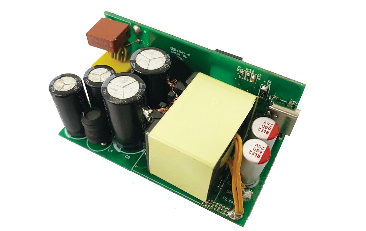
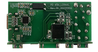 Figure 1: LD966LGQALVE Evaluation Board
Wise-integration has optimized GaN capabilities to make power-electronics technology both greener and more efficient with high-current, high-voltage breakdown and high switching frequency. Its WiseGan® power-integrated circuit (IC) combines several power electronics functions into a single GaN chip for improved speed, efficiency, reliability and cost-effectiveness.
The company opened an office in Taiwan in 2022, and uses 650V GaN/Si technology from Taiwan Semiconductor Manufacturing Co. (TSMC) in its 650V e-mode GaN transistor die with ESD protection.
Wise-integration recently announced the closing of its Series B round of funding totalling €15 million.
The post Wise-integration & Leadtrend Technology Introduce GaN System-in-Package Targeting Rapid Consumer Device Charging appeared first on ELE Times.
Categories: Новини світу мікро- та наноелектроніки
Rohde & Schwarz first to achieve TPAC for NTN NB-IoT RF and RRM conformance test cases
The post Rohde & Schwarz first to achieve TPAC for NTN NB-IoT RF and RRM conformance test cases appeared first on ELE Times.
Categories: Новини світу мікро- та наноелектроніки
Littelfuse Unveils IX4352NE Low-side Gate Driver for SiC MOSFETs and High-power IGBTs
New driver offers tailored turn-on and turn-off timing, minimized switching losses, and
enhanced dV/dt immunity
Littelfuse, Inc., an industrial technology manufacturing company empowering a sustainable, connected, and safer world, is excited to announce the launch of the IX4352NE Low-side SiC MOSFET and IGBT Gate Driver. This innovative driver is specifically designed to drive Silicon Carbide (SiC) MOSFETs and high-power Insulated Gate Bipolar Transistors (IGBTs) in industrial applications.
The key differentiator of the IX4352NE lies in its separate 9 A source and sink outputs, which enable tailored turn-on and turn-off timing while minimizing switching losses. An internal negative charge regulator also provides a user-selectable negative gate drive bias for improved dV/dt immunity and faster turn-off. With an operating voltage range (VDD – VSS) of up to 35 V, this driver offers exceptional flexibility and performance.
One of the standout features of the IX4352NE is its internal negative charge pump regulator, which eliminates the need for an external auxiliary power supply or DC/DC converter. This feature is particularly valuable for turning off SiC MOSFETs, saving valuable space typically required for external logic level translator circuitry. The logic input’s compatibility with standard TTL or CMOS logic levels further enhances space-saving capabilities.
The IX4352NE is ideally suited for driving SiC MOSFETs in various industrial applications such as:- on-board and off-board chargers,
- Power Factor Correction (PFC),
- DC/DC converters,
- motor controllers, and
- industrial power inverters.
Its superior performance makes it ideal for demanding power electronics applications in the electric vehicle, industrial, alternate energy, smart home, and building automation markets.
With its comprehensive features, the IX4352NE simplifies circuit design and offers a higher level of integration. Built-in protection features such as desaturation detection (DESAT) with soft shutdown sink driver, Under Voltage Lockout (UVLO), and thermal shutdown (TSD) ensure the protection of the power device and the gate driver. The integrated open-drain FAULT output signals a fault condition to the microcontroller, enhancing safety and reliability. Furthermore, the IX4352NE saves valuable PCB space and increases circuit density, contributing to overall system efficiency.
Notable improvements over the existing IX4351NE include:- A safe DESAT-initiated soft turn-off.
- A thermal shutdown with high threshold accuracy.
- The charge pump’s ability to operate during thermal shutdown.
The new IX4352NE is pin-compatible, allowing for a seamless drop-in replacement in designs that specify the existing Littelfuse IX4351NE, which was released in 2020.
“The IX4352NE extends our broad range of low-side gate drivers with a new 9 A sink/source driver, simplifying the gate drive circuitry needed for SiC MOSFETs,” commented June Zhang, Product Manager, Integrated Circuits Division (SBU) at Littelfuse. “Its various built-in protection features and integrated charge pump provide an adjustable negative gate drive voltage for improved dV/dt immunity and faster turn-off. As a result, it can be used to drive any SiC MOSFET or power IGBT, whether it is a Littelfuse device or any other similar component available on the market.”
AvailabilityThe IX4352NE Low-side SiC MOSFET and IGBT Gate Driver are available in tube format in 50 per tube or tape and reel format in quantities of 2,000. Place sample requests through authorized Littelfuse distributors worldwide. For a listing of Littelfuse distributors, please visit Littelfuse.com.
For More Information
Additional information on the latest series release is available on the IX4352NE Low-side SiC MOSFET and IGBT Gate Driver product page. For technical questions, please contact one of the following in the Littelfuse Integrated Circuits Division (SBU):
Hugo Guzman, Product Marketing Manager, HGuzman@Littelfuse.com
Klaus Wiedorn, Sr. Technical Marketing Analyst, KWiedorn@Littelfuse.com
The post Littelfuse Unveils IX4352NE Low-side Gate Driver for SiC MOSFETs and High-power IGBTs appeared first on ELE Times.
Categories: Новини світу мікро- та наноелектроніки
Unleashing the potential of industrial and commercial IoT

We’re in the fourth industrial revolution, commonly referred to as Industry 4.0, where advanced technologies are reshaping the landscape of manufacturing and business. The idea of machines communicating with each other, robots milling around, and factories practically running themselves no longer seems like a sci-fi concept.
In the fourth industrial revolution, digital and physical worlds are converging to improve the industrial and commercial (I&C) industries. The Internet of Things (IoT) is a critical player in this revolution, disrupting every facet of the global economy and laying the foundation for a comprehensive overhaul of production, management, and governance systems.
With an estimated annual economic impact ranging from $1.6 trillion to $4.9 trillion by 2025 for factories and retail settings, the rising potential of IoT is becoming increasingly evident as advancements in connectivity open new doors for innovative use cases across the I&C industries.
Despite the rapid advancements in wireless network technologies, companies have been held back from achieving their maximum efficiency and productivity gains due to several operational challenges. Many businesses in industrial and commercial settings face substantial downtime, delayed production, high operating costs, low energy efficiency, and inefficient processes.
So, how can we leverage Industry 4.0’s digital transformation to increase productivity, reduce downtime, lower costs, and drive future growth? The answer may lie in harnessing the power of the I&C IoT.
What’s industrial and commercial IoT?
The Industrial Internet of Things (IIoT) involves the integration of smart technologies and sensors in the industrial sector, enabling the collection and analysis of data to optimize processes, improve worker safety, enhance energy efficiency, improve productivity, and predict potential issues. The IIoT is indispensable for navigating global competition, striking a balance between capturing new business and ensuring sustainable operations.
Commercial IoT encompasses the application of interconnected devices and technologies in the commercial business domain, where the integration of digital solutions aims to enhance retail efficiency, reduce labor costs, and create a seamless omnichannel experience. These advancements in smart retail technology are helping transform traditional business models and increase overall profitability for companies across the globe.

Figure 1 IoT technology will contribute to the growth of commercial industries. Source: Silicon Labs
While such devices may sound out of reach, many exist and are used today for a growing number of I&C applications. In the commercial industry, facility managers seeking to upgrade their estate cost-effectively often use commercial lighting devices like the INGY smart lighting control system that incorporates sensors into luminaires to enable a variety of smart building services without needing an additional infrastructure investment.
Retailers are also adopting electronic shelf label (ESL) devices like the RAINUS InforTab that manage store-wide price automation and reduce operating costs by eliminating hours of tedious human resources. Additionally, asset tracking devices like the Zliide Intelligent Tag can provide fashion retailers with extremely precise location information on how their merchandise moves, helping improve the user experience.
Of course, the commercial industry is not the only application for asset-tracking devices. Machine manufacturers and contractors can also use asset tracking devices like the Trackunit Kin tag that helps connect the entire construction fleet through one simple platform, reducing downtime and costs associated with asset management.
Manufacturers also use smart factory automation devices like CoreTigo’s IO-Link that provide cable-grade, fast, and scalable connectivity for millions of sensors, actuators, and devices at any site worldwide to enable real-time control and monitoring across the entire operational technology.
Likewise, plant and facility managers seeking a comprehensive view of their operations can use predictive maintenance devices such as the Waites plug-and-play online monitoring system to provide a range of sensors and gateways for monitoring and analyzing data, which streamlines device setup and installation.
Benefits of industrial and commercial IoT devices
The growing use of I&C IoT devices could help businesses in the commercial industry make well-informed, real-time decisions, have better access control, and develop more intelligent, efficient, and secure IoT applications. For example, before advanced I&C IoT technology, someone at a retail store had to go out and change the tags on the store shelves if the pricing changed.
Now, with electronic shelf labels, retailers can provide real-time updates. Additionally, by using connected devices and sensors to collect data about a wide variety of business systems, companies can automate processes and improve supply chain management efficiency.
For example, a large retail chain operating hundreds of stores across the country could integrate smart shelf sensors, connected delivery trucks, and a warehouse management system to monitor goods moving through the supply chain in real time. Insights from this data would enable retailers to reduce stockouts, optimize deliveries, and improve warehouse efficiency.
Businesses are also improving control by adopting commercial lighting solutions and wireless access points. With these solutions, businesses can enable indoor location services to track assets and consumer behavior and speed up click-and-collect through shop navigation.
I&C devices also have the potential to positively impact the industrial segment by helping businesses optimize operation efficiency, routing, and scheduling. Prior to predictive maintenance devices, manufacturers had to halt their production line for hours or days if a pump failed and they weren’t planning for it. The repercussions were substantial since every hour of unplanned machine downtime costs manufacturers up to $260,000 in lost production.

Figure 2 IIoT is expected to play a critical role in reshaping the industrial automation. Source: Silicon Labs
Now, with predictive maintenance systems, manufacturers can identify early-stage failures. Moreover, recent advancements in edge computing have unlocked new capabilities for industrial IoT devices, enabling efficient communication and data management.
Machine learning (ML) integration into edge devices transforms data analysis, providing real-time insights for predictive maintenance, anomaly detection, and automated decision-making. This shift is particularly relevant in smart metering, where wireless connectivity allows for comprehensive monitoring, reducing the need for human intervention.
Challenges for industrial and commercial IoT devices
I&C IoT devices have progressed significantly due to the widespread adoption of wireless network technologies, the integration of edge computing, the implementation of predictive maintenance systems, and the expansion of remote monitoring and control capabilities.
Despite all the benefits that I&C IoT devices could bring to consumers, these technologies are not being utilized to their fullest potential in I&C settings today. This is because four significant challenges stand in the way of mass implementation:
- Interoperability and reliability
The fragmented landscape of proprietary IoT ecosystems is a significant hurdle for industrial and commercial industry adoption, and solution providers are addressing this challenge by developing multi-protocol hardware and software solutions.
Multi-protocol capabilities are especially important for I&C IoT devices, as reliable connectivity ensures seamless data flow and process optimization in factories, guarantees reliable connectivity across vast retail spaces, and contributes to consistent sales and operational efficiency. Due to the long product lifecycle, it is also critical for the devices to be compatible with legacy protocols and have the capability to upgrade to future standards as needed.
- Security and privacy
Security and privacy concerns have been major roadblocks in the growth of industrial and commercial IoT, with potential breaches jeopardizing not only data but also entire networks and brand reputations. Thankfully, solution providers are stepping in to equip developers with powerful tools. Secure wireless mesh technologies offer robust defenses against attacks, while data encryption at the chip level paves the way for a future of trusted devices.
This foundation of trust, built by prioritizing cybersecurity from the start and choosing reliable suppliers, is crucial for unlocking the full potential of the next generation of IoT. By proactively shaping their environment and incorporating risk-management strategies, companies can confidently unlock the vast opportunities that lie ahead in the connected world.
- Scalability of networks
Creating large-scale networks with 100,000+ devices is a critical requirement for several industrial and commercial applications such as ESL, street lighting, and smart meters. In addition, these networks may be indoors with significant RF interference or span over a large distance in difficult environments. This requires significant investments in testing large networks to ensure the robustness and reliability of operations in different environments.
- User and developer experience
Bridging the gap between ambition and reality in industrial and commercial IoT rests on two crucial pillars: improving the user experience and the developer experience. If we’re going to scale and deploy this market at the level that we know needs to happen, we need solutions that simplify deployment and management for users while empowering developers to build and scale applications with greater speed and efficiency.
Initiatives like Matter and Amazon Sidewalk are paving the way for easier wireless connectivity and edge computing, but further strides are needed. Solution providers can play a vital role by offering pre-built code and edge-based inference capabilities, accelerating development cycles, and propelling the industry toward its true potential.
Looking ahead
As the industrial and commercial IoT landscape evolves, we are primed for a dynamic and interconnected future. The industrial and commercial IoT industry is poised for continued growth and innovation, with advancements in wireless connectivity, edge computing, AI, and ML driving further advances in industrial automation, supply chain optimization, predictive maintenance systems, and the expansion of remote monitoring and control capabilities.
The semiconductor industry has been quietly helping the world advance with solutions that will help set up the standards of tomorrow and enable an entire ecosystem to become interoperable.
Ross Sabolcik is senior VP and GM of industrial and commercial IoT products at Silicon Labs.
Related Content
- AI Will Empower Industry 4.0 — When It Arrives
- Designer’s Guide to Industrial IoT Sensor Systems
- Smart and Secure Embedded Solutions for IoT Design
- As Industry 4.0 Rises, DevOps Helps Expedite Workflows
- Jumping into Industry 4.0 with Predictive Maintenance Solutions
googletag.cmd.push(function() { googletag.display('div-gpt-ad-native'); });
-->
The post Unleashing the potential of industrial and commercial IoT appeared first on EDN.
Categories: Новини світу мікро- та наноелектроніки
EEVblog 1618 - The Equation For Charge In A Capacitor
Categories: Новини світу мікро- та наноелектроніки
Hear me out
 | What if somebody built an entire calculator using only transistors, resistors, buttons and LEDs. No ICs, no logic gates, no arrays, nothing but pure smd transistors. A calculator with 4 7-segment displays (1+1 for the two input numbers, 2 for the result), 10 inputtable numbers (0-9) and 4 operations (+,-,*,/). Everything would be driven by transistors, including the displays. According to ChatGPT (very reliable, I know), it would take around 3000 components to build such a device. Difficult to make? Yes. Cool to look at? Yes! [link] [comments] |
Categories: Новини світу мікро- та наноелектроніки
Looking inside a laser measurer

Tape measures are right up there with uncooperative-coiling (and -uncoiling) extension cords and garden hoses on the list of “things guaranteed to raise my blood pressure”. They don’t work reliably (thanks to gravity) beyond my arm span unless there’s something flat underneath them for the entire distance they’re measuring. Metal ones don’t do well with curved surfaces, while fabric ones are even more gravity-vulnerable. Speaking of which, the only way to keep a fabric one neatly spooled when not in use is with a rubber band, which will inevitably slip off and leave a mess in whatever drawer you’re storing it in. And when metal ones auto-spool post-use, they inevitably slap, scratch, or otherwise maim your hand (or some other body part) enroute.
All of which explains why, when I saw Dremel’s HSLM-01 3-in-1 Digital Measurement Tool on sale at Woot! for $19.99 late last October, I jumped for joy and jumped on the deal. I ended up buying three of ‘em: one for my brother-in-law as a Christmas present, another for me, and the third one for teardown for all of you:

The labeling in this additional stock photo might be helpful in explaining what you just saw:
 Here’s a more meaningful-info example of the base unit’s display in action:

The default laser configuration is claimed to work reliably for more than five dozen feet, with +/- 1/8-inch accuracy:
 while the Wheel Adapter enables measuring curved surfaces:

and the Tape Adapter (yes, I didn’t completely escape tape, but at least it’s optional and still makes sense in some situations) is more accurate for assessing round-trip circumference (and yes, they spelled “circumference” wrong):
 I mean…look how happy this guy is with his!

Apologies: I dilly-dally and digress. Let’s get to tearing down, shall we? Here’s our victim, beginning with the obligatory outer box shots:


And here’s what the inside stuff looks like:
 Here’s part of the literature suite, along with the included two AAA batteries which I’ll put to good use elsewhere:
 Technology licensed from Arm and STMicroelectronics? Now that’s intriguing! Hold that thought.
 Here’s the remainder of the paper:

And here’s the laser measurer and its two-accessory posse:

This snapshot of the top of the device, as usual accompanied by a 0.75″ (19.1 mm) diameter U.S. penny for size comparison purposes:

is as good a time as any to conceptually explain how these devices work. Wikipedia more generally refers to them as laser rangefinders:
A laser rangefinder, also known as a laser telemeter, is a rangefinder that uses a laser beam to determine the distance to an object. The most common form of laser rangefinder operates on the time of flight principle by sending a laser pulse in a narrow beam towards the object and measuring the time taken by the pulse to be reflected off the target and returned to the sender. Due to the high speed of light, this technique is not appropriate for high precision sub-millimeter measurements, where triangulation and other techniques are often used. It is a type of scannerless lidar.
The basic principle employed, as noted in the previous paragraph, is known as “time of flight” (ToF), one of the three most common approaches (along with stereopsis, which is employed by the human visual system, and structured light, used by the original Microsoft Kinect) to discerning depth in computer vision and other applications. In the previous photo, the laser illumination emitter (Class 2 and <1mW) is at the right, with the image sensor receptor at left. Yes, I’m guessing that this explains the earlier STMicroelectronics licensing reveal. And the three metal contacts mate with matching pins you’ll soon see on the no-laser-necessary adapters.
The bottom is admittedly less exciting:

As are the textured and rubberized (for firm user grip) left and right sides (the two-hole structure at the bottom of the left side is presumably for a not-included “leash”):


I intentionally shot the front a bit off-center to eliminate reflections-of-self from bouncing off the glossy display and case finish:

The duller-finish backside presented no such reflectance concerns:

I have no idea what that white rectangular thing was inside the battery compartment, and I wasn’t brave enough to cut it open for a more thorough inspection (an RFID tracking tag, maybe, readers?):


This closeup of the back label does double-duty as a pictorial explanation of my initial disassembly step:
 Screws underneath, just as I suspected!

You know what comes next…

Liftoff!


We can already see an overview of the laser transmitter function block (complete with a heatsink) at upper right and the receptor counterpart at upper left. Turns out, in fact, that the entire inner assembly lifts right out with no further unscrew, unglue, etc. effort at this point:

From an orientation standpoint, you’re now looking at the inside of the front portion of the outer case. Note the metal extensions of the three earlier noted topside metal contacts, which likely press against matching (flex? likely) contacts on the PCB itself. Again, hold that thought.

Now we can flip over and see the (even more bare) other side of the PCB for the first time:

This is a perspective you’ve already seen, this time absent the case, however:

Three more views from different angles:


And as you may have already guessed, the display isn’t attached to the PCB other than via the flex cable you see, so it’s easy to flip 180°:


Speaking of flipping, let’s turn the entire PCB back over to its back side, now unencumbered by the case that previously held it in place:

Again, some more views from different angles:


See those two screws? Removing them didn’t by itself get us any further along from a disassembly standpoint:

But unscrewing the two other ones up top did the trick:

Flipping the PCB back over and inserting a “wedge” (small flat head screwdriver) between the PCB and ToF subassembly popped the latter off straightaway:


Here’s the now-exposed underside of the ToF module:

and the seen-before frontside and end, this time absent the PCB:


Newly exposed, previously underneath the ToF module, is the system processor, a STMicrolectronics (surprise!…not, if you recall the earlier licensing literature…) STM32F051R8T7 based on an Arm Cortex-M0:
 And also newly revealed is the laser at left which feeds the same-side ToF module optics, along with the image sensor at right which is fed by the optics in the other half of the module (keep in mind that in this orientation, the PCB is upside-down from its normal-operation configuration):

I almost stopped at this point. But those three metal contacts at the top rim of the base unit intrigued me:

There must be matching electrical circuitry in the adapters, right? I figured I might as well satisfy my curiosity and see. In no particular order, I started with my longstanding measurement-media nemesis, the Tape Adapter, first. Front view:

Top view:

Bottom view, revealing the previously foreshadowed pins:

Left and right sides, the latter giving our first glimpse at the end-of-tape tip:


And two more tip perspectives from the back:


Peeling off the label worked last time, so why not try again, right?


Revealed were two plastic tabs, which I unwisely-in-retrospect immediately forgot about (stay tuned). Because, after all, that seam along the top looked mighty enticing, right?

It admittedly was an effective move:

Here’s the inside of the top lid. That groove you see in the middle mates up with the end of the “spring” side of the spool, which you’ll see shortly:

And here’s the inside of the bottom bulk of the outer case. See what looks like an IC at the bottom of that circular hole in the center? Hmmm…

Now for the spool normally in-between those two. Here’s a top view first. That coiled metal spring normally fits completely inside the plastic piece, with its end fitting into the previously seen groove inside the top lid:
 The bottom side. Hey, at least the tape isn’t flesh-mangling metal:

A side view, oriented as when it’s installed in the adapter and in use:

And by the way, about the spindle that fits into that round hole…it’s metallic. Again, hold that thought (and remember my earlier comment about using a rubber band to keep a fabric tape measure neat and tidy?):

Here’s the part where I elaborate on my earlier “forgot about the plastic tabs” comment. At first things were going fine:

 But at this point I was stuck; I couldn’t muscle the inner assembly out any more. So, I jammed the earlier seen flat head screwdriver in one side and wedged it the rest of the way out:


Unfortunately, mangling one of the ICs on the PCB in the process:


Had I just popped both plastic tabs free, I would have been home free. Live and learn (once again hold that thought). Fortunately, I could still discern the package markings. The larger chip is also from STMicroelectronics (no surprise again!), another Arm Cortex-M0 based microcontroller, this time the STM32F030F4. And while at first, reflective of my earlier close-proximity magnetic-tip comment, I thought that the other IC (which we saw before at the bottom of that round hole) might be a Hall effect sensor, I was close-but-not-quite: it’s a NXP Semiconductors KMZ60 magnetoresistive angle sensor with integrated amplifier normally intended for angular control applications and brushless DC motors. In this case, the user’s muscle is the motor! Interesting, eh?
Now for the other, the Wheel Adapter. Front:

Top:

Bottom (pins again! And note that the mysterious white strip seen earlier was pressed into service as a prop-up device below the angled-top adapter):

Left and right sides:


And label-clad back:

I’m predictable, aren’t I?

 Note to self: do NOT forget the two now-exposed plastic tabs this time:

That went much smoother this time:

But there are TWO mini-PCBs this time, one down by the contact pins and another up by the wheel, connected by a three-wire harness:

Unfortunately, in the process of removing the case piece, I somehow snapped off the connector mating this particular mini-PCB to the harness:

Let’s go back to the larger lower mini-PCB for a moment. I won’t pretend to feign surprise once again, as the redundancy is likely getting tiring to the readers, but the main sliver of silicon here is yet another STMicroelectronics STM32F030F4 microcontroller:


The mini-PCB on the other end of the harness pops right out:


Kinda looks like a motor (in actuality, an Alps Alpine sensor), doesn’t it, but this time fed by the human-powered wheel versus a tape spool?


So, a conceptually similar approach to what we saw before with the other adapter, albeit with some implementation variation. I’ll close with a few shots of the now-separate male and female connector pair that I mangled earlier:


And now, passing through 2,000 words and fearful of the mangling that Aalyia might subject me to if I ramble on further, I’ll close, as-usual with an invitation for your thoughts in the comments!
—Brian Dipert is the Editor-in-Chief of the Edge AI and Vision Alliance, and a Senior Analyst at BDTI and Editor-in-Chief of InsideDSP, the company’s online newsletter.
Related Content
- Measuring powerful laser output takes a forceful approach
- Rotational (or linear) measurement using an optical mouse sensor
- Modeling and simulation of magnetoresistive sensor systems (Part 1 of 2)
- MEMS ultrasonic time-of-flight innovation: sensors advance user experiences
- 3D vision gives robots guidance
googletag.cmd.push(function() { googletag.display('div-gpt-ad-native'); });
-->
The post Looking inside a laser measurer appeared first on EDN.
Categories: Новини світу мікро- та наноелектроніки
Cadence Design Systems is empowering a sustainable future with Mission Sustainable Program
Cadence has a mission to help solve technology’s toughest challenges to make a lasting, positive impact on our world, highlighting the company’s commitment to environmental stewardship and empowering employees to become ambassadors for sustainability both within and beyond the organization.
The launch of the Mission Sustainable program in 2023 marked an amplification of this commitment by mobilizing employees from every corner of the company to engage in sustainable development actively. This initiative underscores Cadence’s dedication to environmental care and its vision to cultivate a company-wide culture of sustainability champions.
Innovative Elements of Mission SustainableCadence launched the Mission Sustainable program in 2023 with two key features: the “Live the Brand Sustainably” Quiz and the “Mission Sustainable Ideation Challenge.”
The Live the Brand Sustainably Quiz transformed learning into an exciting competition, deepening employee understanding of Cadence’s ESG efforts and spurring a spirited dialogue around sustainability. This educational contest has significantly bolstered internal engagement with the company’s sustainable vision.

The Mission Sustainable Ideation Challenge harnessed collective creativity by reaching out to our global team to devise innovative solutions in critical sustainability domains such as water conservation, waste reduction, and enhancing supply chain sustainability. Garnering over 150 ideas globally, the challenge culminated in a presentation before Cadence’s leadership, spotlighting the innovation engine driving the company.
A standout project by Indian software architects Gunjan Goel and Naina Dandona, titled “Climate Resilient Software Architecture,” clinched the challenge’s top honor, embodying the inventive spirit Cadence seeks to foster.
Nimish Modi, SVP and GM of Strategy and New Ventures and the executive champion of the program, highlights the foundational belief of Mission Sustainable: “Nurturing sustainability isn’t just a corporate responsibility; it’s a collective endeavor that requires the commitment and passion of every individual. At Cadence, our sustainability initiatives are about reducing our environmental footprint, innovating Cadence technology that delivers sustainability impact for our customers, and empowering our employees to become agents of positive change. Through meaningful engagement and collaboration, we are shaping a more sustainable future for our company and inspiring a broader culture of environmental stewardship.”
Charting a Course Towards Sustainable ExcellenceThe Mission Sustainable challenge has sparked engagement and participation throughout Cadence, encouraging collaboration towards achieving sustainability milestones. Cadence is forging ahead on its sustainability path, leveraging its employees’ diverse talents and innovative thinking, inviting all to be part of a greener, more responsible future.
Read more about Cadence’s environmental, social, and governance programs in the 2023 Cadence ESG Report.
The post Cadence Design Systems is empowering a sustainable future with Mission Sustainable Program appeared first on ELE Times.
Categories: Новини світу мікро- та наноелектроніки
Anritsu Introduces Revolutionary Site Master MS2085A and MS2089A Analyzers: A New Era in Field Testing for Diverse Applications
Anritsu Corporation, a global leader in test and measurement solutions, is excited to unveil its groundbreaking advancements in field testing equipment – the Site Master MS2085A Cable and Antenna Analyzer and the MS2089A with Integrated Spectrum Analyzer. These latest entries to the Anritsu lineup are designed from the ground up to further cement Anritsu’s dominance in the installation and maintenance arena and to also address the multifaceted demands of the general-purpose market. They redefine industry standards for functionality, precision, and user-friendly operation, marking a transformative leap forward in field testing technology.
The Site Master MS2085A and MS2089A encapsulate the pinnacle of modern engineering, combining Anritsu’s extensive experience and commitment to customer-focused innovation. This dual offering merges the functions of cable and antenna analysis with spectrum analysis and monitoring in a seamless, integrated solution. It is tailored to support a wide spectrum of industries, including telecommunications, broadcasting, aerospace, satellite, and defense, facilitating a variety of applications from Distributed Antenna Systems (DAS) and satellite monitoring to interference analysis and routine installation and maintenance tasks.
Highlighted Features and Advantages:- Multi-functional Capability: The Site Master’s integration of cable and antenna analysis alongside spectrum analysis equips professionals with a singular, versatile tool for a wide array of testing and analysis needs. It stands as a comprehensive solution for assessing antenna systems, diagnosing wireless networks, or conducting spectrum signal monitoring.
- Operational Efficiency: Merging multiple testing functions into one device, the Site Master significantly optimizes field testing workflows. This consolidation reduces the need for multiple instruments, streamlines testing processes, and allows for greater achievements in shorter timeframes – effectively enhancing productivity while minimizing operational costs.
- Accuracy and Dependability: Engineered for precision and built to withstand rigorous field conditions, the Site Master ensures consistent, reliable outcomes. Its superior measurement accuracy and robust construction instill confidence in every test result, allowing for precise, informed decisions under any circumstances.
- Advanced Features: With features like Real-Time Spectrum Analysis (RTSA), IQ capture and streaming, and PIM hunting, we’re not just meeting industry standards, we’re creating them.

Raymond Chan, Product Manager at Anritsu Corporation, expresses his enthusiasm: “We are thrilled to launch the Site Master MS2085A and MS2089A, signifying a monumental stride in field testing technology. These innovations underscore our dedication to advancing testing and measurement technologies that not only meet but exceed our customers’ evolving requirements across various sectors. They stand as a testament to Anritsu’s unwavering commitment to excellence, setting a new benchmark for field testing proficiency.”
The Site Master MS2085A and MS2089A Analyzers are now available globally. For detailed information on the products and their capabilities, please visit www.anritsu.com.
The post Anritsu Introduces Revolutionary Site Master MS2085A and MS2089A Analyzers: A New Era in Field Testing for Diverse Applications appeared first on ELE Times.
Categories: Новини світу мікро- та наноелектроніки
Why verification matters in network-on-chip (NoC) design

In the rapidly evolving semiconductor industry, keeping pace with Moore’s Law presents opportunities and challenges, particularly in system-on-chip (SoC) designs. Notably, the number of transistors in microprocessors soared to an unprecedented trillion.
Therefore, as modern applications demand increasing complexity and functionality, improving transistor usage efficiency without sacrificing energy efficiency has become a key goal. Thus, the network-on-chip (NoC) concept has been introduced, a solution designed to address the limitations of traditional bus-based systems by enabling efficient, scalable, and flexible on-chip data transmission.
Designing an NoC involves defining requirements, selecting an architecture, choosing a routing algorithm, planning the physical layout, and conducting verification to ensure performance and reliability. As the final checkpoint before a NoC can be deemed ready for deployment, a deadlock/livelock-free system can be built, increasing confidence in design verification.
In this article, we will dive deeper into a comprehensive methodology for formally verifying an NoC, showcasing the approaches and techniques that ensure our NoC designs are robust, efficient, and ready to meet the challenges of modern computing environments.
Emergence of network-on-chip
NoCs have revolutionized data communications within SoCs by organizing chip components into networks that facilitate the simultaneous transmission of data through multiple paths.
The network consists of various elements, including routers, links, and network interfaces, which facilitate communication between processing elements (PEs) such as CPU cores, memory blocks, and other specialized IP cores. Communication occurs through packet-switched data transmission where data is divided into packets and routed through the network to its destination.
One overview of the complexity of SoC design emphasizes the integration of multiple IP blocks and highlights the need for automated NoC solutions across different SoC categories, from basic to advanced. It advocates using NoCs in SoC designs to effectively achieve optimal data transfer and performance.
At the heart of NoC architecture are several key components:
- Links: Bundles of wires that transmit signals.
- Switches/routers: Devices routing packets from input to output channels based on a routing algorithm.
- Channels: Logical connections facilitating communication between routers or switches.
- Nodes: Routers or switches within the network.
- Messages and packets: Units of transfer within the network, with messages being divided into multiple packets for transmission.
- Flits: Flow control units within the network, dividing packets for efficient routing.
Architectural design and flow control
NoC topology plays a crucial role in optimizing data flow, with Mesh, Ring, Torus, and Butterfly topologies offering various advantages (Figure 1). Flow control mechanisms, such as circuit switching and wormhole flow control, ensure efficient data transmission and minimize congestion and latency.

Figure 1 The topology of an NoC plays an important role in optimizing data flow, as shown with Mesh and Ring (top left and right) and Torus and Butterfly (bottom left and right). Source: Axiomise
Role of routing algorithms in NoC efficiency
As we delve into the complexity of NoC design, one integral aspect that deserves attention is the routing algorithm, the brains behind the NoC that determines how packets move through the complex network from source to destination. They must be efficient, scalable, and versatile enough to adapt to different communication needs and network conditions.
Some of the common routing algorithms for network-on-chip include:
- XY routing algorithm: This is a deterministic routing algorithm usually used in grid-structured NoCs. It first routes to the destination columns along the X-axis and then to the destination rows along the Y-axis. It has the advantages of simplicity and predictability, but it may not be the shortest path and does not accommodate link failures.
- Parity routing algorithm: This algorithm aims to reduce network congestion and increase fault tolerance of the network. It avoids congestion by choosing different paths (based on the parity of the source and destination) in different situations.
- Adaptive routing algorithms: These algorithms dynamically change routing decisions based on the current state of the network (for example, link congestion). They are more flexible than XY routing algorithms and can optimize paths based on network conditions, but they are more complex to implement.
- Shortest path routing algorithms: These algorithms find the shortest path from the source node to the destination node. They are less commonly used in NoC design because calculating the path in real-time can be costly, but they can also be used for path pre-computation or heuristic adjustment.
Advantages of NoCs
- Scalability: As chip designs become more complex and incorporate more components, NoCs provide a scalable solution to manage interconnects efficiently. They facilitate the addition of new components without significantly impacting the existing communication infrastructure.
- Parallelism: NoCs enable parallel data transfers, which can significantly increase the throughput of the system. Multiple data packets can traverse the network simultaneously along different paths, reducing data congestion and improving performance.
- Power consumption: By providing shorter and more direct paths for data transfer, NoCs can reduce the chip’s overall power consumption. Efficient routing and switching mechanisms further contribute to power savings.
- Improved performance: The ability to manage data traffic efficiently and minimize bottlenecks through routing algorithms enhances the overall performance of the SoC. NoCs can adapt to the varying bandwidth requirements of different IP blocks, providing optimized data transfer rates.
- Quality of service (QoS): NoCs can support QoS features, ensuring that critical data transfers are given priority over less urgent communications. This is crucial for applications requiring high reliability and real-time processing.
- Flexibility and customization: The flexibility and customization of the NoC architecture is largely due to its ability to employ a variety of routing algorithms based on specific design requirements and application scenarios.
- Choice of routing algorithm: Routing algorithms in an NoC determine the network path of a packet from its source to its destination. The choice of routing algorithm can significantly impact the performance, efficiency, and fault recovery of the network.
NoC verification challenges
Designing an NoC and ensuring it works per specification is a formidable challenge. Power, performance, and area (PPA) optimizations—along with functional safety, security, and deadlock and livelock detection—add a significant chunk of extra verification work to functional verification, which is mostly centred on routing, data transport, data integrity, protocol verification, arbitration, and starvation checking.
Deadlocks and livelocks can cause a chip respin. For modern-day AI/ML chips, it can cost $25 million in some cases. Constrained random simulation techniques are not adequate for NoC verification. Moreover, simulation or emulation cannot provide any guarantees of correctness. So, formal methods rooted in proof-centric program reasoning are the only way of ensuring bug absence.
Formal verification to the rescue
Industrial-grade formal verification (FV) relies on using formal property verification (FPV) to perform program reasoning, whereby a requirement expressed using the formal syntax of System Verilog Assertions (SVA) is checked against the design model via an intelligent state-space search algorithm to conclude whether the intended requirement holds on all reachable states of the design.
The program reasoning effort terminates with either a proof or a disproof, generating counter-example waveforms. No stimulus is generated by human engineers, and the formal verification technology automatically generates almost an infinite set of stimuli only limited by the size of inputs. This aspect of verifying designs via proof without any human-driven stimulus and with almost an infinite set of stimuli is at the heart of formal verification.
It gives us the ability to pick corner-case issues in the design as well as pick nasty deadlocks and livelocks lurking in the design. Deep interactions in state space are examined quickly, revealing control-intensive issues in the design due to concurrent arbitration and routing traffic in the NoC.
With NoCs featuring numerous interconnected components operating in tandem, simulating the entire range of possible states and behaviors using constrained-random simulation becomes computationally burdensome and impractical. It is due to the intense effort needed for driving stimuli into the NoC that is needed to unravel the state-space interaction, which is not easily possible. This limitation undermines the reliability and precision of simulation outcomes.
Compelling advantages of NoC architectures tout the benefits of integrating FV into the design and verification process using easy-to-understand finite state machine notations and using protocol checkers developed for FV in chip and system integration testing increases confidence and aids error detection and isolation.
The effectiveness of this approach and the challenges of verifying complex systems with large state spaces are emphasized when compared to traditional system simulation successes.
An NoC formal verification methodology
In the complex process of chip design verification, achieving simplicity and efficiency amid complexity is the key. This journey is guided through syntactic and semantic simplification and innovative abstraction techniques.
In addition to these basic strategies, using invariants and an internal assumption assurance process further accelerates proof times, leveraging microarchitectural insights to bridge the gap between testbench and design under test (DUT). This complex verification dance is refined through case splitting and scenario reduction, breaking down complex interactions into manageable checks to ensure comprehensive coverage without overwhelming the verification process.
Symmetry reduction and structural decomposition address verification challenges arising from the complex behavior of large designs. These methods, along with inference-rule reduction and initial-value abstraction (IVA), provide a path that effectively covers every possible scenario, ensuring that even the most daunting designs can be confidently verified.
Rate flow and hopping techniques provide innovative solutions to manage the flow of messages and the complexity introduced by deep sequential states. Finally, black-box and cut-pointing techniques are employed to simplify the verification environment further, eliminating internal logic not directly subject to scrutiny and focusing verification efforts where they are most needed.
Through these sophisticated techniques, the goal of a thorough and efficient verification process becomes a tangible reality, demonstrating the state-of-the-art of modern chip design and verification methods.
Safeguarding NoCs against deadlocks
When setting up NoCs, it’s important for channels to be independent, but it’s not easy to ensure of this. Dependencies between channels can lead to troublesome deadlocks, where the entire system halts even if just one component fails.
Formal verification also contributes to fault tolerance, crucial in NoCs where numerous components communicate. When a component fails, it’s important to understand how close the system is to a permanent deadlock.
Formal verification exhaustively explores all possible system states, offering the best means to ensure fault tolerance. With the right approach, weaknesses of an NoC can be identified and addressed. Catching them early on can save the expensive respin.
Optimizing routing rules to suit the needs is common and critical for performance, but it can be tricky and hard to thoroughly test in simulation. Hundreds of new test cases may emerge just by introducing one new routing rule.
So, modelling all the optimizations in formal verification is crucial. If done properly, it can catch corner case bugs quickly or prove that optimizations behave as expected, preventing unexpected issues.
In the next section, we describe at a high level how some bugs can be caught with formal verification.
Formal verification case studies
Message dependence caused deadlock
A bug originated from a flaw in the flow control mechanism where both request and response packets shared the same FIFO. In this scenario, when multiple source ports initiate requests, the flow control method leads to a deadlock. For instance, when source port 0 sends a request reqs0, consisting of header flit h0req, body b0req, and tail t0req, it gets moved successfully.
Subsequently, the response resps0 made of (h1resp, b1resp, t1resp) intended also for source port 0 arrive, it causes no issue. However, when a subsequent request reqs2 from source port 2 with header flit h2req, body b2req, and tail t2req entered the FIFO, only its header and body move forward, but the tail is blocked from being sampled in the FIFO as the response’s header h2resp has blocked the tail t2req because they arrive in the same clock cycle.
Consequently, source port 2 was left waiting for the tail t2, and found itself blocked by the response header, resulting in a deadlock. Meanwhile, source port 1, also waiting for a response, would never get one, further exacerbating the deadlock situation. This deadlock scenario paralyzed the entire NoC grid, highlighting the critical flaw in the flow control mechanism.

Figure 2 Dependence between request and response causes deadlock. Source: Axiomise
Routing error caused deadlock
In the context of the previously mentioned flow control method, each source port awaits a response after sending a request. However, a deadlock arises due to a flaw in the routing function. When a request is mistakenly routed to an incorrect target port, triggering the assertion of the “wrong_dest” signal, the packet is discarded. Consequently, the source port remains in a state of deadlock, unable to proceed with further requests while awaiting a response that will never arrive.

Figure 3 A deadlock in the flow is caused by a routing error and is unable to proceed. Source: Axiomise
Redundant logic revealing PPA issues
Certain design choices in the routing algorithm, such as prohibiting-specific turns, lead to situations where several FIFOs never have push asserted, and some arbiters handle less than two requestors.
This has been identified during the verification process, revealing that these components—and consequently, millions of gates—are going unused in the design but still occupy chip area and, when clocked, would burn power while not contributing to any performance. Eliminating these superfluous gates significantly reduced manufacturing costs and improved design efficiency.
The case for formal verification in NoC
An NoC-based fabric is essential for any modern high-performance computing or AI/ML machine. NoCs enhance performance by efficient routing to avoid congestion. While NoCs are designed to be efficient at data transmission via routing, they often encounter deadlocks and livelocks in addition to the usual functional correctness challenges between source and destination nodes.
With a range of topologies possible for routing, directing simulation sequences to cover all possible source/destination pairs is almost impossible for dynamic simulation. Detecting deadlocks, starvation and livelocks is nearly impossible for any simulation or even emulation-based verification.
Formal methods drive an almost infinite amount of stimulus to cover all necessary pairs encountered in any topology. With the power of exhaustive proofs, we can establish conclusively that there isn’t a deadlock or a livelock or starvation with formal.
Editor’s Note: Axiomise published a whitepaper in 2022, summarizing a range of practically efficient formal verification techniques used for verifying high-performance NoCs.
Zifei Huang is a formal verification engineer at Axiomise, focusing on NoC and RISC-V architectures.
Adeel Liaquat is an engineering manager at Axiomise, specializing in formal verification methodologies.
Ashish Darbari is founder and CEO of Axiomise, a company offering training, consulting, services, and verification IP to various semiconductor firms.
Related Content
- Introduction to Formal Verification
- What is the future for Network-on-Chip?
- Interconnect (NoC) verification in SoC design
- How formal verification saves time in digital IP design
- Specifications: The hidden bargain for formal verification
googletag.cmd.push(function() { googletag.display('div-gpt-ad-native'); });
-->
The post Why verification matters in network-on-chip (NoC) design appeared first on EDN.
Categories: Новини світу мікро- та наноелектроніки
Microchip Expands its Radiation-Tolerant Microcontroller Portfolio with the 32-bit SAMD21RT Arm Cortex-M0+ Based MCU for the Aerospace and Defense Market
The SAMD21RT MCU is offered in 64-pin ceramic and plastic packages with a 10 mm × 10 mm footprint
Space exploration is experiencing a resurgence with exciting new missions like the highly anticipated Artemis II mission, the recent successful lunar landing missions such as JAXA SLIM and Chandaaryan-3, and New Space deployments in Low Earth Orbit (LEO). Designers require electronic components that meet stringent radiation and reliability standards to operate in the harsh environments found in space. Microchip Technology today announces the SAMD21RT, a radiation-tolerant (RT) Arm Cortex-M0+ based 32-bit microcontroller (MCU) in a 64-pin ceramic and plastic package with 128 KB Flash and 16 KB SRAM.
Designed for space-constrained applications where size and weight are of critical importance, the SAMD21RT is available in a small footprint of 10 mm × 10 mm. Running at up to 48 MHz, the SAMD21RT delivers high-performance processing for harsh environments. The device integrates analog functions including an Analog-to-Digital Converter (ADC) with up to 20 channels, a Digital-to-Analog Converter (DAC) and analog comparators.
The SAMD21RT device builds on Microchip’s existing family of SAMD21 MCUs, which is widely used in industrial and automotive markets. It is also based on Commercial-Off-The-Shelf (COTS) devices, which significantly simplifies the design process when transitioning to a radiation-tolerant device as the design remains pinout compatible. Microchip offers a comprehensive system solution for space applications with many devices that can be designed around the SAMD21RT MCU including FPGAs, power and discrete devices, memory products, communication interfaces and oscillators providing a broad range of options across qualification levels.
To withstand harsh environments including radiation and extreme temperatures, the SAMD21RT can operate in temperatures ranging from −40°C to 125°C and provides a high level of radiation tolerance with a Total Ionizing Dose (TID) capability up to 50 krad and Single Event Latch-up (SEL) immunity up to 78 MeV.cm²/mg.
“The advantage of working with Microchip is that we have the history, knowledge and capability to do the design and testing in house for our radiation-tolerant and radiation-hardened devices,” said Bob Vampola, vice president of Microchip’s aerospace and defense business unit. “We continue to bring newer technologies like Ethernet, AI and ML, which have evolved in the commercial and industrial markets, and improve them with radiation performance to meet the needs of space missions. We also continue to provide higher computing performance and integration of newer technologies into smaller packages, reducing weight and size.”
The low-power SAMD21RT features idle and standby sleep modes and sleepwalking peripherals. Other peripherals include a 12-channel Direct Memory Access Controller (DMAC), a 12-channel event system, various Timer/Counters for Control (TCC), a 32-bit Real Time Counter (RTC), a Watchdog Timer (WDT) and a USB 2.0 interface. Communication options include Serial Communication (SERCOM), I2C, SPI and LIN.
With tens of thousands of parts in orbit, Microchip has been a significant part of space exploration history and is critical to the missions of today and tomorrow. Its products are on the way to the moon as part of the Artemis program and are contributing to the success of the Space Launch System, Orion Spacecraft, Lunar Gateway, Lunar Lander and next-generation spacesuits. To learn more about Microchip’s space heritage, visit the space applications page on the company’s website.
Development ToolsThe SAMD21RT 32-bit MCU is supported by the SAM D21 Curiosity Nano Evaluation Kit, MPLAB® X Integrated Development Environment (IDE) and MPLAB PICkit 5 in-circuit debugger/programmer.
The SAMD21RT 32-bit MCU is available in limited sampling upon request. For additional information, contact a Microchip sales representative.
ResourcesHigh-res images available through Flickr or editorial contact (feel free to publish):
- Application image: flickr.com/photos/microchiptechnology/53641199810/sizes/l
The post Microchip Expands its Radiation-Tolerant Microcontroller Portfolio with the 32-bit SAMD21RT Arm Cortex-M0+ Based MCU for the Aerospace and Defense Market appeared first on ELE Times.
Categories: Новини світу мікро- та наноелектроніки
Wireless Power in the Kitchen
Authors: Akshat JAIN, STMicroelectronics India, Fabrizio Di FRANCO, STMicroelectronics, Italy, Martin DENDA, Rene WUTTE, STMicroelectronics Austria, Bruno TISSERAND, STMicroelectronics, France
Wireless power is going to introduce significant innovations in kitchens, making them smarter, sleeker and more space-efficient. Appliances from simple low-power juicers to blenders or kettles, and others that require up to 2.2 kW of power will benefit by eliminating power cords thanks to the new standard “Ki Cordless Kitchen” that is set to be released by the Wireless Power Consortium. The key driver of rapid adoption is interoperability. All certified Ki transmitters and appliances will follow defined safety protocols and work with each other, regardless of the brand, device type, or version of Ki they use.
The Ki transmitter can also be considered a smart induction cooktop that will not only power Ki receivers but also operate standard induction utensils like heating a pan. Ki enables smart communication between transmitters and appliances based on Near Field Communication (NFC) providing auxiliary power, bi-directional data paths, advanced control features, authentication and protections (FOD) and it is essential for interoperability. The block diagram of the Ki Cordless Kitchen concept block diagram is highlighted in Figure 1.
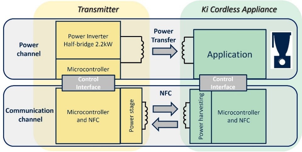 Figure 1: Ki Cordless Kitchen concept block diagram
STMicroelectronics, a global semiconductor leader serving customers across the wide spectrum of electronics applications, has been participating in the Ki Cordless Kitchen standard since the beginning and is ready with the Ki Cordless Kitchen power transmitter reference design i.e. STEVAL-KITXCB. The reference design consists of a power inverter board, auxiliary power supply board, an NFC board, inverter microcontroller board, a power coil, NFC antenna and GUI display board as shown in Figure 2. Thanks to the modular design approach, it is easy for users to test and debug the various sections involved.
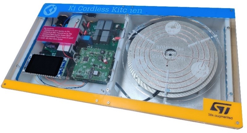 Figure 2: Ki Cordless Kitchen evaluation kit (STEVAL-KITXCB)
The main power board comprises an inverter stage based on half-bridge topology. The IGBTs during power transfer switch between 26 to 74 kHz. The power inverter board is connected to a power coil and is digitally controlled by the STM32G474RET6 microcontroller, which specifically addresses the needs of digital power conversion applications thanks to the High-resolution timer peripheral and a rich and advanced integrated analog. The NFC communication between the Ki transmitter and Ki receiver is managed by ST25R3916, a high-performance NFC universal device which is mounted on a dedicated daughter card. The NFC antenna is connected to the NFC daughter card. The auxiliary power supply is managed by an off-line flyback circuitry based on VIPer318, high voltage converter ensuring compactness and very low standby consumption to generate 24V DC. The interconnection between the main power inverter board and the daughter cards of the evaluation kit is shown in Figure 3. The inverter stage is based on STGWA50IH65DF trench gate field-stop 650 V IH series IGBT, featuring very low Vcesat and Eoff to ensure high efficiency at high switching frequency and supported by the robust half-bridge gate driver L6491D, provided with high driving current source and sink capability.
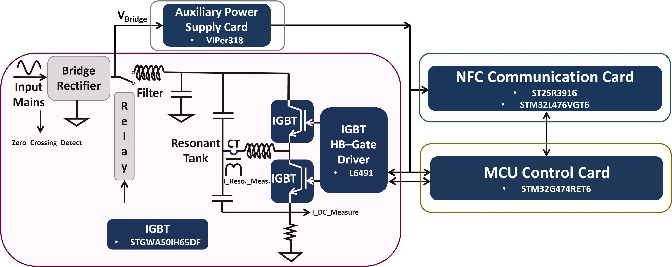 Figure 3: Ki Cordless Kitchen transmitter reference design (STEVAL-KITXCB) – Block Diagram
The Ki Kitchen standard protocol is managed by a dedicated STM32L476VGT64 microcontroller mounted on an NFC daughter card and it communicates over UART with the STM32G474RET6 microcontroller, which is managing power inverter stage. During startup when the Ki receiver/appliance is brought on top of induction hub the Ki transmitter will supply the initial energy to power the User interface of the appliance through NFC and establish a communication carrier as shown in Figure 4. And when the Ki receiver/appliance is switched ON (requesting power from the Ki transmitter) from its user interface, then the auxiliary power transfer from NFC stops, and the power inverter of the Ki transmitter transmits the power including auxiliary power to the Ki receiver via the principle of induction.
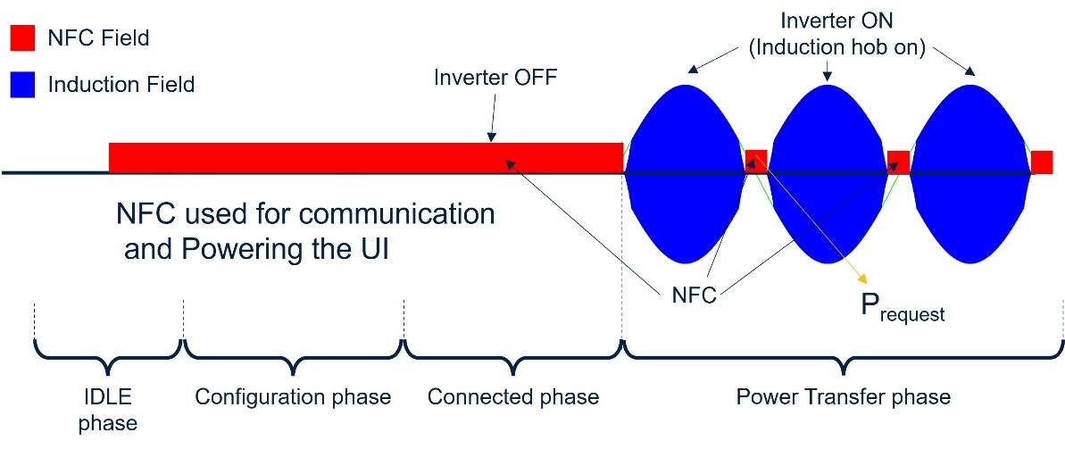 Figure 4: NFC Communication – Idle state and power transfer state
To prevent interference between NFC and wireless induction power transfer during the power transfer state, the wireless induction power transfer is switched completely off during the mains crossing and NFC becomes active as shown in Figure 4.
Ki receiver vs Induction Utensil (Pan/Pot)
The standard induction utensils are made of ferromagnetic materials. The bottom of an induction utensil (pan/pot) can be treated as an induction coil with one winding and low load resistance where received power is dissipated. So, the power transmitter coil and utensil can be considered a transformer in which the induction utensil acts as a shorted secondary (load). An alternating current is made to flow through the transmitter resonant power coil, which leads to the generation of an oscillating magnetic field. The magnetic field induces an electric current inside the induction utensil.
The Ki receiver mainly consists of a resonant power coil, resonant capacitor, NFC circuitry and Ki receiver/appliance circuitry. For the Ki transmitter the power coil is fixed but for the Ki receivers, the size of the power coil varies depending on the power requirements. To maximize the energy transfer, the Ki receiver must be tuned to the transmitter’s resonant frequency. Now, there will be two resonance points: one of the Ki transmitter and the other of the Ki receiver. To have better efficiency, the transmitter needs to operate at a second resonant frequency, but that doesn’t guarantee the maximum power required by the Ki receiver. To transmit the desired power the Ki transmitter needs to shift to the first resonant frequency. The resonant shift is managed by the STM32G474RET6 microcontroller control algorithm.
To shorten the development time and let customers evaluate products in the final application, STMicroelectronics offers a reference design (STEVAL-KITXCB) for the transmitter and is working on the reference design for the different types of receivers. The hardware design files and firmware source code are available with developer-friendly license terms. For more details, please contact the STMicroelectronics sales office.
The post Wireless Power in the Kitchen appeared first on ELE Times.
Categories: Новини світу мікро- та наноелектроніки
Relay and solenoid driver circuit doubles supply voltage to conserve sustaining power

A generally accepted fact about relays and solenoids is that after they’re driven into the actuated state, only half as much coil voltage and therefore only one fourth as much coil power, are required to reliably sustain it. Consequently, any solenoid or relay driver that continuously applies the full initial actuation voltage to merely sustain is wastefully squandering four times as much power as the job requires.
The simplest and cheapest (partial) solution to this problem is shown in Figure 1.

Figure 1 Basic driver circuit where C1 actuates, current-halving R1 sustains, then C1 discharges through R1 during Toff.
Wow the engineering world with your unique design: Design Ideas Submission Guide
But as is often true of “simple and cheap,” Figure 1’s solution suffers from some costs and complications.
- While R1 successfully cuts sustaining current by half, it dissipates just as much power as the coil as it does so. Consequently, total sustaining power is ½ rather than ¼ of actuating power, so only half of the theoretical power savings are actually realized.
- When the driver is turned off, a long recovery delay must be imposed prior to the next actuation pulse to allow C1 enough time to discharge through R1. Otherwise, the next actuation pulse will have inadequate amplitude and may fail. This effect is aggravated by the fact that, during actuation, C1 charges through the parallel combination of R1 and Rm, but during Toff it discharges through R1 alone. This makes recovery take twice as long as actuation.
Figure 2 presents a better performing, albeit less simple and cheap, solution that’s the subject of this Design Idea.

Figure 2 Q1 and Q2 cooperate with C to double VL for actuation, Q2 and D2 sustain, then Q3 rapidly discharges C through R to quickly recover for the next cycle.
Actuation begins with a positive pulse at the input, turning Q1 on which drives the bottom end of the coil to -VL and turns on Q2 which pulls the top end of the coil to +VL. Thus, 2VL appears across the coil, insuring reliable actuation. As C charging completes, Schottky diode D2 takes over conduction from Q1. This cuts the sustaining voltage to ½ the actuation value, and therefore drops sustaining power to ¼.
At the end of the cycle when the incoming signal returns to V0, Q3 turns on, initiating a rapid discharge of C through D2 and R. In fact, recovery can easily be arranged to complete in less time than the relay or solenoid needs to drop out. Then no explicit inter-cycle delay is necessary and recovery time is therefore effectively zero!
Moral: You get what you pay for!
But what happens if even doubling the VL logic rail still doesn’t make enough voltage to drive the coil and a higher supply rail is needed?
Figure 3 addresses that issue with some trickery described in an earlier Design Idea: Driving CMOS totem poles with logic signals, AC coupling, and grounded gates.

Figure 3 Level shifting Q4, R1, and R2 are added to accommodate ++V > VL.
Stephen Woodward’s relationship with EDN’s DI column goes back quite a long way. Over 100 submissions have been accepted since his first contribution back in 1974.
Related Content
- Driving CMOS totem poles with logic signals, AC coupling, and grounded gates
- Booster circuit enables reliable solenoid operation
- Solenoid-protection circuit limits duty cycle
- Simple solenoid driver is adaptable and efficient
googletag.cmd.push(function() { googletag.display('div-gpt-ad-native'); });
-->
The post Relay and solenoid driver circuit doubles supply voltage to conserve sustaining power appeared first on EDN.
Categories: Новини світу мікро- та наноелектроніки
Ethernet adapter chips aim to bolster AI data center networking

At a time when scalable high-bandwidth and low-latency connectivity is becoming critical for artificial intelligence (AI) clusters, the new 400G PCIe Gen 5.0 Ethernet adapter chips aim to resolve connectivity bottlenecks in AI data centers.
Broadcom claims its 400G PCIe Gen 5.0 chips are the first Ethernet adapters built with 5-nm process technology. “We recognize the significance of fostering a power-efficient and highly connected data center for AI ecosystem,” said Jas Tremblay, VP and GM of the Data Center Solutions Group at Broadcom.
The 400G PCIe Gen 5.0 Ethernet adapters deliver higher rack density by driving passive copper cables up to five meters. Moreover, these Ethernet adapters employ low-latency congestion control technology and innovative telemetry features while equipped with a third-generation RDMA over Converged Ethernet (RoCE) pipeline.
These Ethernet adapters are built on Broadcom’s sixth-generation hardened network interface card (NIC) architecture. Their software is designed to be vendor agnostic; it supports a broad ecosystem of CPUs, GPUs, PCIe and Ethernet switches using open PCIe and Ethernet standards.

Ethernet adapter chips must resolve connectivity bottlenecks as cluster sizes grow rapidly in AI data centers. Source: Broadcom
According to Patrick Moorhead, chief analyst at Moor Insights and Strategy, as the industry races to deliver generative AI at scale, the immense volumes of data that must be processed to train large language models (LLMs) require even larger server clusters. He added that Ethernet presents a compelling case as the networking technology of choice for next-generation AI workloads.
AI-centric applications are reshaping the data center networking landscape, and Broadcom’s new 400G PCIe Gen 5.0 Ethernet adapters highlight the crucial importance of devices operating in the high-bandwidth, high-stress network environment that characterizes AI infrastructure.
Related Content
- AI Trolls for Data Center Woes
- PCIe Eyes Road Ahead with AI, Automotive
- Backplane tutorial: RapidIO, PCIe and Ethernet
- PCI Express vs. Ethernet: A showdown or coexistence?
- Accelerated Infrastructure Simply the Next Evolution of Data Center Infrastructure
googletag.cmd.push(function() { googletag.display('div-gpt-ad-native'); });
-->
The post Ethernet adapter chips aim to bolster AI data center networking appeared first on EDN.
Categories: Новини світу мікро- та наноелектроніки
EEVblog 1617 - Architectural LED Lighting Build + Test
Categories: Новини світу мікро- та наноелектроніки
Homemade circuit board to replace mechanical pinball machine selector.
 | My grandparents got this pinball machine in the mid 60s. There was a mechanical spinner that would register and record a highlighted letter if you hit a certain thing when it was lit up. It used a mechanical spinning device that broke, so my grandfather built the circuit board as a sort of logic puzzle after taking apart the mechanical device and figuring out what it needed. don’t know anything about electronics, but I thought y’all might be interested [link] [comments] |
Categories: Новини світу мікро- та наноелектроніки
Pages


![[link]](https://i.redd.it/gzvpmi9snu1d1.jpeg)