
ELE Times

How Can the High Voltage Intelligent Battery Shunt Reference Design Benefit You?
Courtesy: Element 14
Introduction
Accurate current measurement is a critical aspect of modern electrical engineering. Precision is essential everywhere – from battery management systems (BMS) to industrial automation. Traditional sensing methods are inadequate when temperatures fluctuate, leading to unreliable readings.
That’s where shunt resistors come to the rescue. These components produce a small, measurable voltage drop that reflects the amount of current flowing through them. However, their performance can be influenced by changes in temperature, which alter resistance and distort measurements. The temperature coefficient of resistance (TCR) quantifies this change, making low TCR shunt resistors essential for high precision applications.
Vishay’s WSBE8518 shunt resistor exemplifies such precision. Vishay offers the HV-IBSS-USB reference design – a sophisticated tool that simplifies testing and integration – to streamline its evaluation. This article explores the function of shunt resistors, the significance of low TCR, the impact of thermal drift, and how the HV-IBSS-USB reference design empowers engineers to achieve accurate current sensing in demanding environments.
Understanding Shunt Resistors in Current Sensing
A shunt resistor, also known as a current shunt resistor or an ammeter shunt, is a low resistance component placed in series with a load to measure voltage drop when current flows through it. This voltage drop, measured by an analogue-to-digital converter (ADC), is directly proportional to the current, enabling accurate current measurement using Ohm’s Law.
Shunt resistors are vital in precision current sensing across a wide range of high-reliability applications. These include monitoring charge and discharge cycles in BMS for electric vehicles (EV), energy storage systems, and portable devices, regulating output and detecting overcurrent in power supplies and motor control systems. Renewable energy setups like solar inverters and wind turbines ensure accurate power flow measurement, while industrial automation provides critical feedback for diagnostics and system reliability. They are also indispensable in network UPS systems, power meters, and high-precision environments such as aerospace and defence applications, where even minor deviations in current measurement can have critical consequences.
Selecting a shunt resistor involves balancing its resistance value, power rating, and TCR. For instance, the WSBE8518, with a 100 μΩ resistance and 36 W power rating at 70 °C, produces a 50 mV drop at 500 A – making it suitable for high current applications while maintaining accuracy. The WSBE series can support up to 1825 A with no noticeable resistance shift.
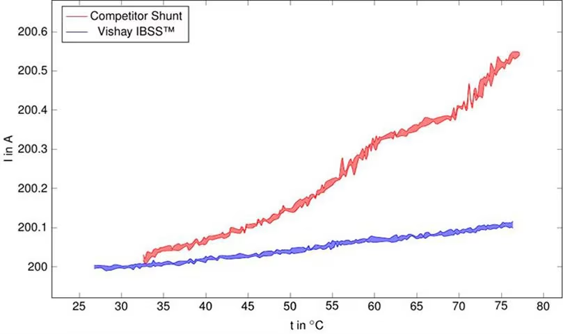 Figure 1: A comparison of current measurement stability over temperature between Vishay’s Intelligent Battery Shunt System (IBSS) and a competing shunt
Figure 1 demonstrates that as the temperature rises from 25 °C to 80 °C, the standard shunt (in red) shows a current reading drift from 200 A to over 200.6 A, while Vishay’s (in blue) remains nearly flat at 200 A, highlighting its superior thermal stability. Vishay also delivers cleaner, less noisy measurements, unlike the standard shunt’s non-linear, noisier signal response.
Why Does TCR Matter in Precision Sensing?
Resistance isn’t constant—it changes with temperature. The TCR quantifies this change, expressed in parts per million per degree Celsius (ppm/°C). In simple terms, TCR tells us how much a resistor’s value will drift as the temperature fluctuates.
If a resistor has a positive TCR, its resistance increases with rising temperature. A negative TCR means resistance decreases as it gets warmer. In either case, too much variation can compromise measurement accuracy. A low TCR is critical in precision current sensing, especially in systems where even the slightest error can cascade into larger problems. Due to increased electron scattering, most metals naturally see resistance rise with temperature. However, specialized alloys — such as the manganese-copper used in Vishay’s WSBE8518 shunt resistor —can achieve remarkably stable performance, with TCRs as low as ± 10 ppm/°C. This makes them ideal for applications demanding high accuracy under wide temperature swings.
For instance, a 1 mΩ shunt with a TCR of ± 50 ppm/°C will experience a resistance change of ± 5 µΩ over a 100 °C temperature swing, which is equivalent to ± 0.5 % of its nominal resistance. That may seem insignificant, but in high precision environments such as battery charge balancing or power regulation, such deviations can skew current readings and disrupt system performance. The following equation calculates the maximum change in resistance value for a given TCR:
R = R0 X 1 [ 1 + α(T-T0)]
where,
R = final resistance
R0 = initial resistance
α = TCR
T = final temperature
T0 = initial temperature
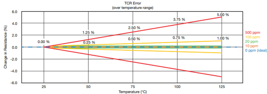 Figure 2: This graph compares different TCR levels as a percentage change in resistance versus increasing temperature from 25 °C
The benefits of low TCR are:
- Improved measurement accuracy: With resistance remaining stable across temperature variations, current sensing becomes more precise
- Better thermal stability: Minimal resistance drift, even under fluctuating ambient conditions or due to self-heating from applied power
- Ideal for high precision circuits: Supports applications that require consistent performance over wide temperature ranges
- Enhanced performance in harsh environments: Suitable for military and high-temperature electronics where reliability under thermal stress is critical
- Minimizes error in Kelvin configurations: Particularly advantageous in 4-terminal setups in which precise voltage sensing is critical
Figure 3 illustrates the superior thermal stability of WSBE series resistors (NiCr and CuMn) compared to standard shunt resistors. While the standard shunt exhibits a large resistance drift over temperature (indicative of poor TCR), the WSBE resistors maintain almost constant resistance across a broad thermal range.
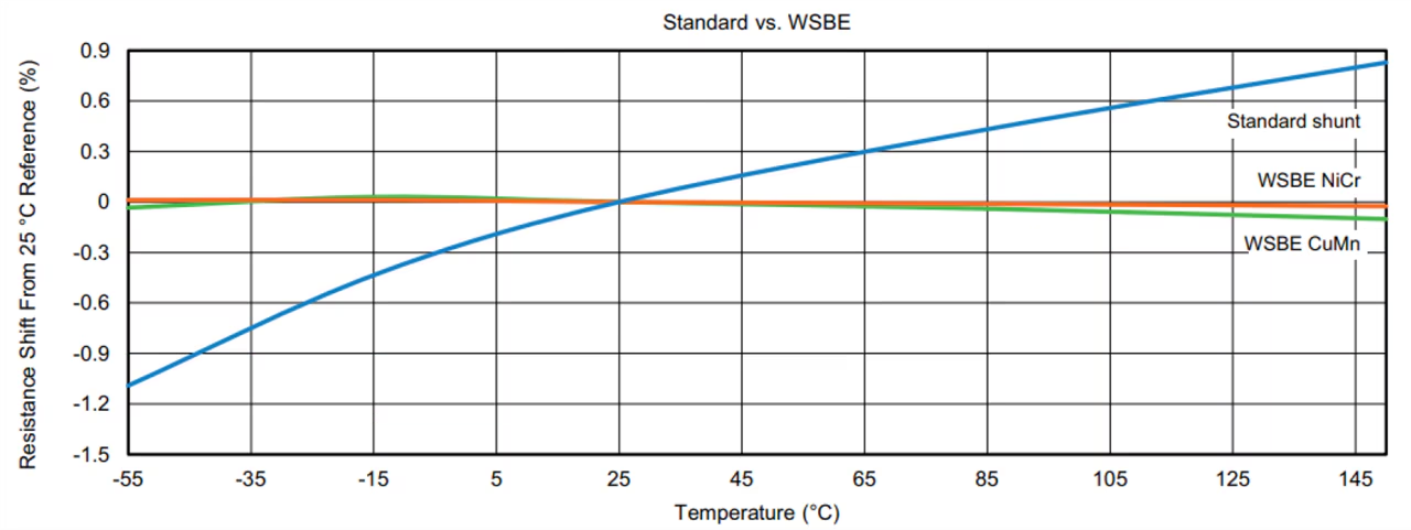 Figure 3: TCR comparison chart (WBSE series vs a standard shunt resistor)
Understanding Thermal Drift in Current Sensing
Thermal drift refers to changes in a component’s electrical characteristics caused by fluctuations in temperature. In shunt resistors, thermal drift alters resistance, directly affecting current measurement accuracy. For instance, copper, with a TCR of 3900 ppm/°C, can exhibit a 39 % resistance change over a 100 °C temperature range, severely compromising precision. Low TCR materials, such as the manganese-copper alloy in the WSBE8518, reduce this effect, maintaining high measurement accuracy.
Thermal drift can also arise from self-heating due to power dissipation during operation. Vishay’s HV-IBSS-USB mitigates this by combining a low TCR shunt with an efficient circuit design, minimizing temperature-induced errors. Kelvin (4-terminal) connections further enhance accuracy by reducing the impact of high TCR copper terminals, enabling consistent and repeatable measurements.
How the Reference Design Works
The HV-IBSS-USB reference design features two isolated domains: an HV analog front-end and an LV digital control section. Powered and interfaced via USB, the LV side hosts a microcontroller that manages data acquisition and communication. Power is transferred to the HV domain through a charge pump, where precision 22-bit sigma-delta ADCs and carefully selected analog components enable high-resolution current and voltage measurements.
The design compensates for thermal drift through automatic gain and offset calibration, ensuring accuracy across temperature variations. A dedicated voltage divider feeds the voltage signal directly to the ADC, eliminating amplifier drift. An NTC-based converter transmits a PWM signal across the isolation barrier for temperature monitoring. Data is available via a virtual COM port, auto-detected over USB, enabling seamless integration with PC-based tools.
- Current measurement: a third-order delta-sigma modulator converts the voltage drop across the WSBE8518 shunt into a digital signal, with automatic gain and offset calibration. The shunt’s TCR (10 ppm/°C) outperforms the analog circuitry’s drift (33.6 ppm/°C), ensuring high accuracy
- Voltage measurement: a 22-bit sigma-delta ADC measures voltage, divided by the CDMA2512 resistor to fit the ADC’s range
Temperature measurement: an NTC thermistor and multivibrator convert temperature to a frequency signal, transmitted as a PWM signal to the microcontroller
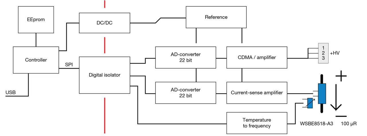 Figure 5: Functional block diagram of the HV-IBSS-USB
Application: EVs
In BMS for EVs and other compact mobility vehicles such as electric two-wheelers, precise current measurement is critical for monitoring charge and discharge cycles, balancing cells, and ensure safe, efficient operation. The HV-IBSS-USB facilitates the evaluation of the WSBE8518 shunt in these demanding environments. Installed in series with the high voltage battery pack, the shunt accurately measures currents up to 500 A, which is ideal for applications where currents routinely exceed 100 A.
The reference design’s USB-C interface enables real-time data logging, allowing engineers to analyze current flow, detect anomalies, and fine-tune battery management algorithms. The WSBE8518’s low TCR ensures accurate measurements even as operating temperatures rise during rapid charging or high load discharge. Voltage measurements spanning 10 V to 850 V and integrated temperature sensing provide additional data for detecting faults or optimizing power distribution.
A typical application circuit places the shunt between the EV battery and the drive or charging system. The HV-IBSS-USB’s HV+ and HV + terminals connect to the shunt’s Kelvin terminals, and the USB-C port links to a computer for data acquisition and analysis.
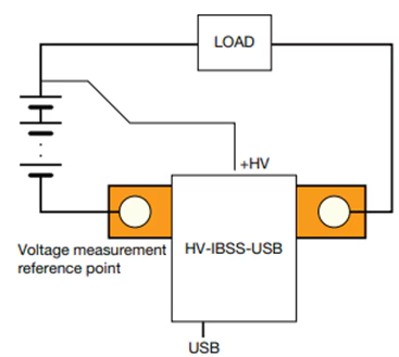 Figure 6: Typical application circuit
Conclusion
As current sensing requirements continue to tighten across EVs, energy storage, and high-power industrial systems, accuracy can no longer be left vulnerable to temperature effects and component drift. Vishay’s HV-IBSS-USB reference design, built around the ultra-low-TCR WSBE8518 shunt resistor, addresses this challenge head-on by combining material stability, Kelvin sensing, high-resolution ADCs, and intelligent calibration in a ready-to-evaluate platform. By minimizing thermal drift and simplifying high-voltage, high-current measurements, the design enables engineers to validate performance quickly, reduce development risk, and deploy more reliable battery and power management systems. In applications where every milliamp matters, the HV-IBSS-USB offers a practical pathway from precision measurement theory to real-world, production-ready accuracy.
The post How Can the High Voltage Intelligent Battery Shunt Reference Design Benefit You? appeared first on ELE Times.
The Move to 48 Volts in Transportation
Courtesy: Avnet
| Key Takeaways:
● 48V systems are being adopted in mobility, industrial, data centres, and automotive ● Higher voltage brings multiple benefits ● New 48V motor control kit offers flexibility and efficiency ● Battery management included |
Shifting to 48V isn’t just about higher voltage. What stands out here is how that shift enables lighter designs, longer battery life, and more efficient operation. Think drones that fly further, autonomous robots that run longer without a recharge, and electric vehicles that pack more punch without bulking up.
For OEMs looking at a new product line or planning upgrades, that’s more than a technical specification; it’s a competitive factor. Getting ahead of this voltage transition could mean catching the next wave in smart transportation and industrial automation.
The market’s responding, not just in automotive, but across sectors like logistics, warehousing, and even consumer robotics.
Put 48V on your roadmap
For teams evaluating roadmap priorities, the takeaway is that aligning with this voltage shift isn’t optional. It’s quickly becoming a baseline expectation for future-ready platforms.
NXP has introduced a high-power 48V motor control kit, and there’s quite a bit under the hood here. You’ve got flexibility for controlling single three-phase, dual three-phase, and single six-phase setups, plus compatibility with resolver, hall, and encoder sensors. That means it’s well-positioned for teams with complex motor demands. Those motors could be driving a range of applications, from drones to autonomous or guided robots.
From a strategic standpoint, having isolated communication and redundant power supply isn’t just a feature; it’s risk mitigation. Fault protection for things like overcurrent and overheating? That’s a game-changer for operational uptime. Add functional safety to the mix. It’s built for both industrial and automotive standards, so teams don’t have to choose between performance and compliance.
Development kit availability
Launch timing is crucial. NXP’s development kit is available from December for early access, but the full rollout lands in January. Contact your Avnet representative to register your interest. NXP is also bundling standard drivers and control libraries, so the barrier to entry is lower for engineering teams.
For OEMs that need deeper customisation, there’s a premium software tier with extra safety features and source code. The architecture is modular, too: controller board, adapter board, power stage, and heat sink, with motors left out for flexibility. That setup is deliberate, letting customers tailor the kit to their own requirements, rather than locking them into a one-size-fits-all hardware solution.
 The NXP development kit will be generally available from January 2026, with early access available by contacting your Avnet representative.
NXP MCUs are at the core, plus a GUI for streamlined control. It’s aimed at making deployment straightforward, whether for prototyping or scaling up production. That level of integration should make it easier for teams to hit aggressive timelines while still meeting compliance and quality bars.
Battery management for 48V systems
Let’s shift the focus to battery management. If you’re investing in next-gen mobility or industrial systems, BMS is at the heart of every decision. What’s new here is the scale. The product family now covers everything from 12 volts all the way up to 1500 volts, but the 48V range is the sweet spot for cost and flexibility. That’s not just for cars; it’s a fit for industrial energy storage, drones, and autonomous robots.
That creates a broader footprint, but what’s the real differentiator between these 48V solutions and the legacy setups? First, you’re seeing devices like the BMA 7518 that are exclusive to 48V, with others bridging up to higher voltages in industrial use. Certification’s a key lever. Everything’s aiming for ISO 26262 on the automotive side and IEC 61508 for industrial. Compliance isn’t just a checkbox; it moves the needle on market access and risk.
There’s a new software stack for active cell balancing, and “battery passport” tools are being rolled out to keep up with European compliance. Secure protocols are another layer, making sure the system’s ready for upcoming requirements. NXP is not just filling out the product line; it’s building for future-proofing and regulatory headwinds.
Early access to 48V solutions
Avnet is working with NXP to provide early access for select customers. If you’re aiming to build momentum before January, this is a real lever for market entry. By prioritising hands-on pilots and direct feedback loops, teams catch issues or feature requests early in the cycle.
If you are evaluating 48V systems, contact your Avnet representative to find out how you could benefit from these exciting developments.
The post The Move to 48 Volts in Transportation appeared first on ELE Times.
Adoption of Electric Motorcycles: A Challenging Ride Ahead
India’s tryst with electric two-wheelers began as early as the 1990s, but meaningful momentum only arrived decades later. Early policy interventions—such as subsidies offered by the Ministry of New and Renewable Energy (MNRE) between 2010 and 2012—laid the groundwork. The launch of the FAME (Faster Adoption and Manufacturing of Electric Vehicles) scheme further accelerated adoption, drawing both startups and legacy manufacturers into the electric mobility race.
Yet, despite this progress, one segment remains conspicuously underdeveloped: electric motorcycles. A joint NITI Aayog–TIFAC study published in June 2022 estimates that India’s two-wheeler manufacturing capacity could exceed 20 million units annually by 2030. However, electric motorcycles account for only a negligible fraction of this future potential.
Royal Enfield’s Electric Bet Rekindles DebateAs India’s foremost motorcycle manufacturer, Royal Enfield’s move into electric mobility represents more than product diversification—it marks a fundamental technological transition for a brand long associated with large-displacement engines, mechanical character, and long-distance touring capability. Entering the electric motorcycle space forces a redefinition of performance, shifting the emphasis from displacement and acoustics to torque delivery, thermal control, software, and system integration.
The company has signalled its electric intent through the Flying Flea platform, with two derivatives planned for launch after 2026. Beyond the product itself, the real story lies in the underlying technology stack Royal Enfield is building for the electric era.
According to Matt Cardenas, Head of EV Product Strategy at Royal Enfield, much of the vehicle’s technology has been developed in-house to optimise user experience. Over 200 engineers are engaged in powertrain development, with 42 patents already filed. The company has also partnered directly with NXP and Snapdragon to co-develop motorcycle-specific chips—an uncommon move in the two-wheeler industry.
For a company built on the appeal of powerful combustion motorcycles, Royal Enfield’s electric strategy suggests a broader reimagining of power itself. In the absence of exhaust notes and mechanical mass, performance is being reconstructed through torque curves, thermal discipline, and digital intelligence. How successfully this engineering-first approach translates into rider acceptance may ultimately determine whether electric motorcycles can move beyond the margins of India’s two-wheeler market.
Where Does India’s Electric Motorcycle Market Stand?In August 2025, NITI Aayog convened a high-level meeting with major two-wheeler OEMs—Hero MotoCorp, Bajaj Auto, TVS Motor, Ola Electric, Ather Energy, and Revolt Motors—to explore strategies for improving electric motorcycle adoption.
The current market structure highlights the challenge. Internal combustion engine (ICE) motorcycles still account for nearly two-thirds of India’s two-wheeler market. Electric scooters, by contrast, have achieved around 15% penetration within the EV segment and now represent almost one-third of all two-wheelers sold. Electric motorcycles, however, contribute just 0.1% of the total two-wheeler market, according to NITI Aayog.
It’s partly because motorcycle manufacturing is dominated by some heavy-loaded challenges, ranging from the weight of the battery to efficiency and experience.
The Weight of the Battery ProblemBattery weight remains one of the most fundamental constraints. Unlike four-wheelers, motorcycles are highly sensitive to mass distribution. For long-distance and off-road riding in particular, maintaining balance, agility, and stability becomes increasingly complex as battery size grows.
Engineers must carefully position the battery to preserve handling characteristics while reinforcing the frame without adding excessive weight. Ergonomics also demands rethinking, as the traditional engine layout is replaced by a bulkier energy storage system. Suspension and braking systems require complete recalibration to match the altered dynamics of an electric powertrain. In effect, designing an electric motorcycle is far more complex than simply swapping an engine for a motor.
Reflecting the same idea, Ather’s leadership has noted that practical and cost considerations currently favour electric scooters over bikes in India — an observation directly linked to the challenges electric motorcycles face in matching affordability and everyday utility.
Efficiency Gains That Don’t Fully TranslateOn paper, electric motors are vastly more efficient than ICEs, converting 80–90% of electrical energy into motion, compared to just 20–30% for combustion engines. Regenerative braking and fewer moving parts further enhance theoretical efficiency.
However, these advantages shrink when evaluated on a well-to-wheel basis. Petrol has a far higher energy density by weight than today’s lithium-ion batteries. A small fuel tank can deliver long range with minimal mass, while an equivalent amount of stored electrical energy adds substantial weight. For long-distance riding at sustained speeds, the heavier battery pack can negate much of the motor’s inherent efficiency advantage, resulting in shorter real-world range than ICE motorcycles.
Transmission, Maintenance, and the Rider’s BondElectric scooters have benefited from simple, gearless drivetrains that translate easily into electric architectures. Motorcycles, especially those with gears, face greater design and manufacturing complexity. This also affects maintenance and repair—areas of particular importance to India’s motorcycle culture, where self-repair and aftermarket modifications are deeply ingrained. Limited service familiarity and proprietary components can dampen enthusiasm among seasoned riders.
The Sound of SilenceFor many long-distance and enthusiast riders, motorcycles are as much about emotion as engineering. The sound, vibration, and mechanical feedback of a combustion engine form a core part of the riding experience. Electric motorcycles, with their near-silent operation, can feel less visceral—even if they deliver superior acceleration.
That said, this argument is not universal. Electric bikes offer tangible benefits: drastically reduced noise pollution, smoother power delivery, and instant torque that can feel both controlled and exhilarating. For a new generation of riders, these attributes may redefine what performance and pleasure mean on two wheels.
A Weak Global Reference EcosystemGlobally, electric motorcycles lack the ecosystem support that helped electric scooters scale. The NITI Aayog study notes the absence of learning spillovers from international markets. While India benefited from mature Chinese supply chains and proven designs in e-scooters, no comparable global blueprint exists for electric motorcycles. As a result, manufacturers must build R&D capabilities largely from scratch.
Only a handful of players—Revolt Motors, Ultraviolette Automotive, Oben Electric, and Matter Motors—are currently active in India’s electric motorcycle space. This contrasts sharply with the success of Ola Electric and Ather Energy in the scooter segment. Internationally, the picture has also dimmed, highlighted by the bankruptcy of Italian high-performance EV motorcycle maker Energica in October 2024. While brands like Kawasaki and Zero remain prominent globally, volumes remain limited.
Also, executives from Bajaj Auto’s electric two-wheeler business have acknowledged that the industry initially struggled with supply chain readiness and cost structures, and that building a sustainable EV business requires a measured approach rather than aggressive cash burn — indirectly underscoring how complexity and cost are barriers for electrifying performance-oriented two-wheelers.
The Road AheadFor now, innovation appears to be the only force capable of sustaining momentum in electric motorcycles. Breakthroughs in battery chemistry, thermal management, lightweight materials, and modular platforms will be critical. Until governments worldwide offer stronger policy support—through targeted subsidies, charging infrastructure, and R&D incentives—electric motorcycles are likely to remain a passion project rather than a mass-market reality.
The ride ahead, much like the machines themselves, will demand balance, patience, and relentless engineering ingenuity.
The post Adoption of Electric Motorcycles: A Challenging Ride Ahead appeared first on ELE Times.
Edge AI Chipsets: How On-Device Intelligence Is Reshaping Embedded System Design
The cloud-first model for embedded systems is becoming a legacy architecture. We’re moving away from simply piping data to remote servers and instead shifting the entire decision engine onto the bare metal. Driven by specialised Edge AI silicon-like NPUs and accelerated RISC-V cores, this evolution allows us to bake autonomous logic directly into sensors and controllers. In a production environment, on-device AI is a functional requirement, not a luxury. As NVIDIA CEO Jensen Huang noted in his 2025 GTC keynote, “The next wave is already happening… Robotics, which has been enabled by physical AI-AI that understands the physical world, is the new era,” marking a definitive shift toward intelligence that lives where the action occurs.
Here is why Several factors make on-device AI critical today:
- Solving Latency: In robotics or power-grid monitoring, a cloud round-trip is a system failure. You need deterministic, sub-millisecond responses that only local inference provides.
- Cutting the Bandwidth Tax: Constant streaming drains batteries and budgets. Local processing means we only transmit the “meaning,” not the raw noise, making massive IoT fleets cost-effective.
- Hardened Privacy: For medical or industrial IP, data in transit is a liability. Keeping telemetry on the silicon is the most effective way to ensure confidentiality. Cristiano Amon, CEO of Qualcomm, reinforces this, stating: “When you do the processing on the device, it’s immediate. You don’t have to wait. It’s private. It’s your data. It’s your personal graph that stays with you.
- True Autonomy: Your hardware shouldn’t brick when the Wi-Fi drops. Edge AI ensures the machine stays smart in remote or “noisy” environments.
These factors collectively make Edge AI an essential enabler of modern embedded intelligence.
Architectural Distinctions of Edge AI Chipsets
Edge AI chipsets differ from conventional microcontrollers (MCUs) and CPUs in architectural intent and operational efficiency. Core characteristics include:
- AI Accelerators (NPUs/VPUs): Dedicated engines built for neural-network inference (convolutions, matrix multiplications) that significantly exceed CPUs in speed and power efficiency.
- Heterogeneous SoC Architectures: A combination of CPU (control tasks), NPU (AI inference), and sometimes GPU (parallel processing), ensures optimised resource allocation across workloads.
- Model Optimisation: Deep learning models can be deployed on devices with limited resources without experiencing significant accuracy loss thanks to techniques like quantisation, pruning, and compression.
- Power & Thermal Management: Edge AI can function within stringent power and temperature constraints thanks to dynamic voltage and frequency scaling, low-power modes, and thermal improvements.
- Security & Reliability Features: Protection of sensitive operations-particularly in industrial deployments and critical infrastructure achieved through measures such as memory isolation, secure boot processes, and hardware-level tamper-resistant design.
By combining these features, edge-AI chipsets make intelligent behaviour feasible on devices previously incapable of complex decision-making.
Transforming Embedded System Design
The introduction of Edge AI fundamentally alters embedded system design:
- From Reactive to Cognitive Systems: Traditional embedded devices follow deterministic logic to detect defects, predict equipment failures and monitor the electronic equipment. Edge AI enables them to perceive, classify, and act autonomously.
- Real-Time Autonomy: With local inference, devices operate independently of cloud connectivity, critical for industrial, safety-critical, or remote applications.
- Distributed Intelligence & Scalability: Large IoT deployments can now distribute AI across nodes, reducing network load and ensuring real-time responsiveness.
- Energy and Bandwidth Efficiency: Local processing cuts down on data transmission, which saves energy and money and makes the system less reliant on centralized infrastructure.
- Cross-Layer Co-Design: Hardware-software co-design is now essential. Teams must optimise model architecture, memory allocation, runtime scheduling, and power management from the outset.
Edge AI thus transforms embedded systems from simple controllers into autonomous, intelligent agents capable of learning and decision-making.
Real-World Applications
Edge AI chipsets are already revolutionising multiple sectors:
- Industrial Automation & Smart Manufacturing: Vision-based defect detection, predictive maintenance, anomaly detection, and real-time monitoring of inverters, EV chargers, and SMPS.
- Embedded Vision & IoT: Smart cameras, object detection, robotics, drones, and smart sensors with on-device analytics.
- Consumer Electronics & Wearables: Offline voice recognition, gesture detection, and biometric authentication while preserving privacy.
- Energy & Power Electronics: Autonomous monitoring of power converters, predictive fault detection, and safety-critical decisions in EV and renewable energy systems.
- Agriculture & Remote Infrastructure: Edge AI sensors classify crop health, monitor environmental conditions, and operate autonomously in rural or low-connectivity areas.
These applications illustrate that Edge AI is no longer experimental – it’s a practical enabler for real-world intelligence in embedded systems.
Challenges and Considerations
While Edge AI presents opportunities, several challenges require careful engineering:
- Resource Constraints: Limited compute, memory, and power require model optimisation, which may impact accuracy or capability.
- Hardware Heterogeneity: Diverse SoCs and NPUs make deployment across platforms complex.
- Thermal and Power Management: Continuous inference can generate heat and consume power, impacting device lifespan.
- Security & Trust: Edge devices handling sensitive data must ensure secure boot, encryption, and tamper resistance.
- Model Lifecycle Management: Updating and maintaining models across fleets of devices, especially in remote locations, is a significant operational challenge.
- Design Complexity: Effective deployment demands collaboration between ML engineers, hardware designers, and embedded software developers.
Addressing these challenges is essential for scalable, robust, and efficient Edge AI implementations.
Emerging Trends & the Road Ahead
Edge AI chipsets are evolving rapidly:
- TinyML and Micro-Edge Devices: Ultra-low-power NPUs enable AI on minimal sensors and microcontrollers.
- Chiplet-Based Modular SoCs: Modular architectures combining CPUs, AI accelerators, and memory provide scalable, upgradeable solutions.
- Cross-Layer Automation: Improved toolchains for quantisation, pruning, scheduling, and deployment reduce manual tuning and accelerate development.
- Hybrid Edge-Cloud Models: On-device inference combined with federated learning or cloud aggregation balances autonomy with long-term model improvement.
- Enhanced Security: Trusted execution environments and secure hardware primitives protect distributed edge deployments.
These trends point toward embedded systems that are intelligent, autonomous, energy-efficient, and scalable across industries.
India’s Emerging Edge AI Ecosystem
India is rapidly contributing to the global Edge AI landscape. Startups and MNCs like Netrasemi, Mindgrove Technologies, InCore Semiconductors, and MosChip Technologies are developing edge-AI SoCs, NPUs, and embedded solutions tailored for industrial, automotive, and IoT applications. With government initiatives like Digital India and Make in India, combined with academic research, the country is fostering innovation in Edge AI for both domestic and global markets.
Conclusion
Edge AI chipsets are changing what we expect from embedded devices. Work that once had to be pushed to a central system can now be handled directly where the data is produced. This allows equipment to react immediately, even in environments where connectivity is unreliable or power is limited. Designing such systems is no longer just a matter of selecting a processor and writing code; it involves careful trade-offs between performance, power use, reliability, and long-term maintenance, with security built in from the start. As AI visionary Andrew Ng recently summarised, “The future AI wealth doesn’t belong to those who own the largest GPU clusters but to those who know how to use the smallest models to solve the most specific problems… Edge computing and small models are the wealth keys.
For engineers in the embedded domain, this is a practical turning point rather than a theoretical one. Devices are moving beyond fixed, single-purpose roles and taking on more responsibility within distributed setups. Edge AI enables the development of autonomous and efficient systems. These solutions deliver the consistent reliability required by various industries.
The post Edge AI Chipsets: How On-Device Intelligence Is Reshaping Embedded System Design appeared first on ELE Times.
Quantum-Safe Hardware: Why the Cybersecurity Deadline Is Closer Than the Quantum Breakthrough
The world’s digital infrastructure is quietly approaching a cryptographic inflexion point. For decades, global cybersecurity has relied on a small set of mathematical assumptions, most notably RSA and elliptic-curve cryptography. These assumptions underpin everything from cloud authentication and mobile networks to payment systems, defence communications, and digital identity. Quantum computing threatens not to weaken these foundations, but to invalidate them entirely.
What makes this transition uniquely dangerous is not the arrival of quantum computers themselves, but the mismatch between how fast cryptography can be broken and how slowly hardware trust systems can be replaced. This is not a software problem that can be patched overnight. It is a hardware lifecycle problem measured in decades. As quantum research accelerates and post-quantum cryptography standards solidify, a hard truth is emerging across the industry: quantum-safe hardware must be deployed well before quantum computers can break encryption. Waiting for certainty is, paradoxically, the fastest path to systemic insecurity.
From Mathematical Risk to Engineering Reality
Quantum computing represents a rare technological disruption where the threat is mathematically inevitable, not probabilistic. Shor’s algorithm does not weaken RSA or elliptic-curve cryptography; it nullifies them. Once fault-tolerant quantum computers emerge, today’s cryptographic foundations collapse outright. More critically, attacks need not be real-time: encrypted data captured today can be decrypted years later under the “harvest now, decrypt later” model.
As Ali El Kaafarani, CEO of PQShield, has consistently argued, the industry’s mistake is treating post-quantum cryptography as a future software upgrade rather than a present hardware engineering challenge. Once quantum decryption is possible, compromise is retroactive; you don’t lose today’s secrets, you lose yesterdays. This reality has shifted focus from cryptographic theory to what can be implemented in silicon. While many PQC schemes exist on paper, only a narrow set survives real-world constraints of memory, power, latency, and side-channel resistance. Lattice-based algorithms such as NIST-standardised Kyber and Dilithium are currently the most hardware-viable, though they still impose significant demands. Other approaches, like code-based cryptography, struggle with impractically large key sizes that overwhelm secure hardware resources.
Why Hardware, Not Software, Is the Real Battleground
Cryptography is enforced by hardware roots of trust, HSMs, secure elements, TPMs, SIMs, and embedded controllers that underpin secure boot, identity, and key protection. Post-quantum cryptography breaks the assumptions these systems were built on: larger keys and heavier computation quickly expose the limits of hardware optimised for RSA and ECC. While software can absorb this overhead, hardware-bound systems cannot.
This is where “crypto-agility” fractures. Many platforms claim algorithm agility, but in practice, it exists only at the firmware or API layer, not in silicon. As Todd Moore, Vice President of Data Security Products at Thales, has noted, true crypto-agility is about whether hardware can evolve without becoming a performance bottleneck. In high-throughput environments, first-generation “PQC-ready” hardware often works functionally but not economically, forcing a choice between degraded performance and early replacement. Crypto-agility is no longer a software feature; it is a physical property of hardware architecture.
The Myth of Universal Crypto-Agility
In response to quantum risk, many vendors describe their products as “crypto agile.” In practice, crypto-agility has often meant that software can be updated, while the underlying hardware remains fixed. That model is breaking down. True crypto-agility in the post-quantum era requires hardware that was designed with uncertainty in mind: spare compute capacity, flexible accelerators, sufficient secure memory, and firmware update paths that are themselves resistant to quantum attacks. Much of the hardware deployed today, particularly older HSMs and embedded roots of trust, does not meet this bar.
Newer platforms from vendors such as Thales and Entrust are moving toward genuinely post-quantum-ready architectures, but even here, the industry is candid that early PQC support is only a first step. In many environments, especially high-throughput systems like certificate authorities and telecom authentication servers, performance collapses when PQC is layered onto hardware never designed for it. The uncomfortable implication is that a significant portion of deployed cryptographic hardware will ultimately need physical replacement, not because it is insecure today, but because it cannot scale securely tomorrow.
The Long-Life Device Problem: Secure Boot and Identity
Quantum risk becomes existential when hardware is expected to remain trusted for 15–20 years. Industrial equipment, telecom infrastructure, vehicles, medical devices, and defence systems often outlive multiple cryptographic generations. If the firmware-signing keys protecting these systems become quantum-breakable mid-lifecycle, attackers gain the ability to install malicious updates that appear fully legitimate.
To address this, hardware designers are rethinking trust from the ground up. Secure boot chains are increasingly being designed around hybrid verification models, where classical and post-quantum signatures coexist during a long transition period. Device identity is shifting toward roots of trust that can support PQC natively, rather than bolting it on later.
Equally important is the ability to migrate trust anchors in the field. Hardware that cannot rotate its cryptographic identity without physical access becomes a liability the moment quantum attacks become practical. In this sense, quantum-safe hardware is no longer just a security feature; it is a prerequisite for product longevity.
Scale Changes Everything
Post-quantum cryptography is feasible at a small scale. The real challenge emerges at volume. Larger keys and signatures mean more data moving through networks, more bytes stored in certificates, and more cycles spent on verification. In isolation, these costs are manageable. At the scale of global telecom networks, payment systems, and cloud platforms, they become systemic.
Cloud providers have already found that naïve PQC deployment can inflate handshake sizes enough to affect latency and throughput. Telecom operators face similar issues in authentication signalling, where milliseconds matter. This is why hybrid cryptography combining classical and post-quantum algorithms has become the dominant near-term strategy. Hardware acceleration is the critical enabler here. When PQC is supported at the silicon level, much of the overhead becomes manageable. When it is not, performance penalties cascade across the system.
The Real Deadline No One Wants to Announce
Public timelines often place cryptographically relevant quantum computers in the early to mid-2030s. Internally, many security leaders plan as if the deadline is earlier. The reason is simple: hardware migration takes time. From design and validation to certification and deployment, replacing cryptographic hardware across critical infrastructure can take a decade. Waiting for definitive proof that quantum computers can break RSA guarantees that the response will come too late. A pragmatic consensus is forming across the industry. By the second half of this decade, all new cryptographic hardware procurement must be quantum-safe by design. By the end of the decade, high-value infrastructure must complete the transition. Anything beyond those risks turning today’s encrypted data into tomorrow’s breach archive.
As Marco Pereira, Global Head of Cybersecurity at Capgemini, has emphasised about quantum risk “Quantum readiness isn’t about predicting a date, it’s about managing irreversible risk. Every encrypted asset today could become tomorrow’s breach if organisations delay adopting post-quantum protections.
Quantum-safe hardware is not driven by fear of the unknown. It is driven by certainty that cryptography is bounded by physics, certainty that hardware lifecycles are slow, and certainty that data longevity outlasts algorithm lifetimes. The organisations that navigate this transition successfully will not be those that deploy post-quantum cryptography fastest in software, but those that redesign their hardware roots of trust early, with crypto-agility, scale, and long-term integrity at the core. In the quantum era, cybersecurity failures will not arrive with alarms or outages. It will arrive quietly, years after the data was first captured. The only winning strategy is to make that data permanently useless before the quantum key ever turns.
The post Quantum-Safe Hardware: Why the Cybersecurity Deadline Is Closer Than the Quantum Breakthrough appeared first on ELE Times.
SQL Server IoT 2025: Why It Matters for Embedded and OEM Systems
Courtesy: Arrow Electronics
The new SQL Server IoT 2025 is now available! If you build devices, appliances, or embedded systems that ship with a database inside, SQL Server IoT 2025 is worth a serious look. It brings the SQL Server 2025 engine into long-life, fixed-function products. You get the full engine, the same AI features, the same JSON and vector capabilities, and the same security improvements. The only difference is that it is packaged and licensed for OEM and embedded scenarios.
In my experience supporting embedded customers, the pattern is consistent. More data at the edge, tight security requirements, long product lifecycles, and pressure to support AI without adding cloud dependencies. SQL Server IoT 2025 helps you handle those problems without changing how you design your systems. You can use the same T-SQL, drivers, tools, containers, and development workflow.
AI where your device runs
The biggest change in SQL Server IoT 2025 is the built-in AI stack. The database now supports a native vector type, semantic search, hybrid search, and local or remote model execution. You can generate embeddings inside the engine, and you can run AI agents through a secure REST endpoint that SQL Server manages.
Nothing in this requires a cloud connection unless you choose to use one. You can keep models local by using Ollama or ONNX Runtime. You can also call cloud models through Azure OpenAI or OpenAI.
For embedded systems, this means you can build features that previously required a cloud round-trip. Examples include local anomaly detection, troubleshooting assistance, natural language search of manuals or logs, and smarter automation. If you already store your device data in SQL Server, the new vector features let you use that data immediately.
Security that matches modern requirements
The platform is secure out of the box. SQL Server IoT 2025 carries forward the security updates from SQL Server 2025. That includes TLS 1.3, TDS 8.0, PBKDF hashing, managed identities, and stricter defaults. This helps you ship hardware that is ready for audit and compliance checks. For teams in healthcare, manufacturing, or other controlled industries, this reduces significant design risk.
Performance improvements that help small systems
Most devices in the field run on constrained compute, so predictable behaviour underload becomes more important than raw horsepower. SQL Server IoT 2025 benefits from improvements like optimised locking, Lock After Qualification, tempdb governance, faster failover, and reduced contention during heavy workloads.
Your device can run more predictable workloads with fewer stalls. It starts faster, handles concurrency better, and gives you cleaner behaviour when something in the system misbehaves.
Better ways to move data out of the device
You also get Change Event Streaming, which pushes changes directly to Azure Event Hubs. The engine streams committed transactions without extra system tables. This helps when your design needs low-latency reporting or coordination with services outside the device.
If you use Microsoft Fabric, SQL Server IoT 2025 supports database mirroring directly into OneLake. That gives you a simple path to analytics or long-term storage without writing ETL code.
Developer workflow stays simple
Stability in the toolchain is just as important as stability in the engine. SQL Server IoT 2025 uses the same drivers, SSMS, VS Code extension, containers, and deployment workflow. You also get the new JSON type, JSON indexing, RegEx functions, Base64 utilities, and improved T-SQL functions that SQL Server 2025 introduces.
When an upgrade is worth it
If you are trying to decide whether this upgrade is worth it, these are the points that usually guide the decision:
- If your device is running SQL Server 2014 or 2016, you are past or near the end of mainstream support, and the extended support runway is shrinking fast. SQL Server IoT 2025 offers a long-life option with a modern engine, stronger security, and a cleaner feature set for long-term maintenance. You also get improvements like accelerated recovery, better indexing behaviour, and up-to-date drivers.
- If your product roadmap includes AI features or if customers are asking for analytics without sending data off the device, SQL Server IoT 2025 gives you a built-in way to handle that.
- If your company is standardising on Fabric or Azure Arc, IoT 2025 fits neatly into that architecture.
If your design team is trying to reduce custom code around queues, logs, or sync processes, IoT 2025 reduces that work.
The post SQL Server IoT 2025: Why It Matters for Embedded and OEM Systems appeared first on ELE Times.
Microchip Releases Plastic Transient Voltage Suppressors for A&D Applications
Microchip Technology announced the release of its JANPTX family of non-hermetic plastic Transient Voltage Suppressor (TVS) devices that meet the MIL-PRF-19500 qualification, offering high-reliability protection for aerospace and defence applications. These TVS devices are the first in the industry to achieve MIL-PRF-19500 qualification in a plastic package, offering engineers a lightweight, cost-effective solution without sacrificing stringent military performance requirements. The JANPTX product line is available in voltage ranges from 5V to 175V and includes five variants: JANPTX1N5555UJ, JANPTX1N5558UG, JANPTX1N5629AUJ, JANPTX1N5665AUG, JANPTX1N5907UG and JANPTX1N5907UJ.
With a high peak pulse power rating of 1.5 kW and clamping response times measured at less than 100 picoseconds in internal tests, the JANPTX family is designed to help ensure the safety and reliability of sensitive electronic components in demanding environments. Designed for surface mounting, these unidirectional TVS devices deliver protection against voltage transients such as lightning strikes, electrostatic discharge (ESD), and electrical surges.
Key Features of the TVS Devices
- Surface-mount unidirectional TVS design
- Can suppress transients up to 1,500W at 10/1000 µs
- Capable of clamping transients in less than 100 ps
- Working voltage range: 5V to 175V
- Military qualification: MIL-PRF-19500/716
- Equivalent hermetic packages available for surface mount and thru-hole
- Weight: ~0.25 grams
Development Tools
The JANPTX devices are supported by various SPICE models, which enable the virtual prediction and simulation of a circuit’s behaviour, eliminating the need for time-consuming physical prototyping and redesigns.
The post Microchip Releases Plastic Transient Voltage Suppressors for A&D Applications appeared first on ELE Times.
Týr-the-Pruner: Search-based Global Structural Pruning for LLMs
Courtesy: AMD
Key Takeaways:
- End-to-end global structural pruning: Týr-the-Pruner jointly optimises pruning and layer-wise sparsity allocation, avoiding two-stage global ranking pipelines.
- Multi-sparsity supernet with expectation-aware error modelling: Layers are pruned at multiple sparsity levels and evaluated collectively to capture cross-layer dependencies.
- Coarse-to-fine evolutionary search under a fixed sparsity budget: Sparsity-shift mutations preserve global constraints while progressively refining resolution (12.5% → 1.56%).
- Taylor-informed, backprop-free local pruning: First- and second-order saliency guides structured pruning with minimal functional drift.
- Near-dense accuracy with real hardware gains: Up to 50% parameter reduction retains ~97% accuracy on Llama-3.1-70B, accelerating inference on AMD Instinct GPUs.
As large language models (LLMs) scale into the tens and hundreds of billions of parameters, pruning has re-emerged as a critical lever for improving inference efficiency without sacrificing accuracy. AMD’s Týr-the-Pruner advances this frontier with a search-based, end-to-end framework for global structural pruning, delivering up to 50% parameter reduction while retaining ~97% of dense accuracy on Llama-3.1-70B—a new state of the art among structured pruning methods.
Accepted to NeurIPS 2025, the work also demonstrates tangible inference speedups on AMD Instinct GPUs, reinforcing pruning’s relevance not just as a compression technique, but as a practical path to deployment-scale efficiency.
Why global sparsity matters
Local structural pruning is appealing for its simplicity and efficiency: layers are pruned independently, often allowing even hundred-billion-parameter models to fit on a single device. However, this approach enforces uniform per-layer sparsity, overlooking how errors and redundancies propagate across layers.
Existing “global” pruning methods attempt to address this by first ranking substructures across layers and then pruning accordingly. While intuitive, this two-stage pipeline breaks end-to-end optimisation and struggles to capture inter-layer interactions.
Týr-the-Pruner flips the paradigm. Instead of ranking structures before pruning, it first constructs a multi-sparsity supernet and then searches directly for the optimal layer-wise sparsity distribution under a fixed global budget—yielding a truly end-to-end global pruning strategy.
Inside Týr-the-Pruner: How It Works
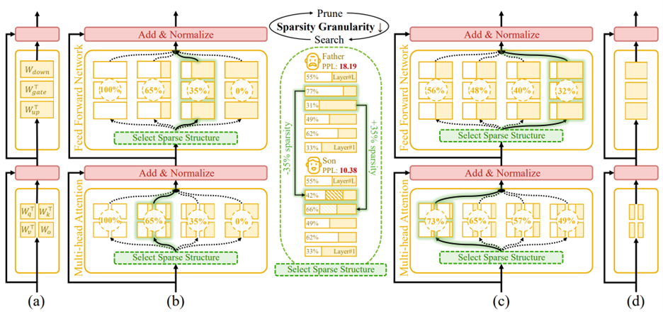
Figure 1. An overview of Týr-the-Pruner. Large language models (a) will be effectively locally pruned across multiple sparsity ratios and constructed into a supernet (b). An iterative prune-and-search strategy will be used to select the optimal sparse structure for each layer while maintaining a target overall sparsity ratio: pruning and sparsity-shift-driven evolutionary search are implemented iteratively with a coarse-to-fine sparsity interval granularity (c). Ultimately, the post-pruned LLM with the optimal sparsity distribution (d) is obtained.
Building a Reliable Supernet
The process begins by locally pruning every layer across multiple sparsity levels. Týr employs Taylor-informed saliency (first- and second-order) alongside backprop-free weight adjustment, applied progressively to minimise performance perturbations.
To ensure that different pruned variants remain mutually consistent, the framework introduces expectation-aware error accumulation, addressing the otherwise ambiguous error propagation that arises when multiple pruned copies coexist within a supernet.
Coarse-to-Fine Global Search
Once the supernet is established, Týr performs an evolutionary sparsity-shift search. Each mutation preserves the global sparsity budget—for example, making one layer slightly denser while another becomes equivalently sparser. Candidate models are evaluated using distillation-based similarity metrics over hidden activations and logits.
A naïve fine-grained search would be intractable: for an 80-sublayer model, even modest sparsity resolution would imply an astronomically large configuration space. Týr sidesteps this with an iterative coarse-to-fine strategy:
- The search begins with a coarse sparsity interval (12.5%) and just nine candidates per layer.
- After identifying a strong sparsity pattern, the search recentres and halves the interval (12.5% → 6.25% → 3.13% → 1.56%).
- After four iterations, Týr reaches fine-grained sparsity resolution while keeping each iteration’s effective search space manageable.
This design steadily narrows the search, accelerates convergence, and efficiently uncovers the optimal global sparsity distribution.
Results: Accuracy and efficiency on AMD hardware
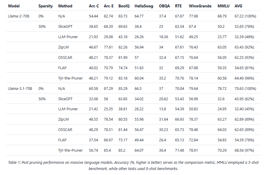
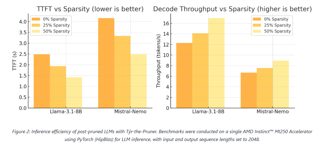
Across models and benchmarks, Týr-the-Pruner consistently preserves near-dense accuracy while delivering meaningful efficiency gains on AMD Instinct MI250 accelerators.
At 50% sparsity, the method retains 96–97% average accuracy on 70B-scale models—outperforming structured pruning approaches such as SliceGPT, LLM-Pruner, and FLAP. On smaller models, the runtime benefits are equally compelling: for Llama-3.1-8B and Mistral-Nemo, pruning cuts time-to-first-token by up to 1.75× and boosts decode throughput by up to 1.38×.
These results position pruning as a first-class optimisation technique for large-scale LLM inference, particularly on modern accelerator architectures.
Practical Considerations: Memory and Search Efficiency
While supernets can be large, Týr keeps memory usage close to that of a single dense model by storing pruned substructures on disk and loading only the active subnet into high-bandwidth memory. Disk footprints remain manageable—around 40 GB for 7–8B models and ~415 GB for 70B models—with older artefacts cleaned up between iterations.
The evolutionary search itself is computationally efficient. Evaluations proceed under progressively increasing token budgets (2K → 16K → 128K), converging rapidly thanks to the coarse-to-fine schedule. For 8B-scale models, a single search iteration completes in a few hours, keeping overall runtime well within practical limits.
Summary
Týr-the-Pruner represents a shift in how global structural pruning is approached. By unifying pruning and sparsity allocation into a single, end-to-end search process—and combining it with expectation-aware error modelling and coarse-to-fine optimisation—the framework achieves both high accuracy retention and real-world inference acceleration.
With up to 50% parameter reduction and ~97% accuracy preserved on Llama-3.1-70B, Týr-the-Pruner demonstrates that global pruning can be both principled and practical—setting a new benchmark for structured pruning in the era of large-scale LLM deployment.
The post Týr-the-Pruner: Search-based Global Structural Pruning for LLMs appeared first on ELE Times.
Global Semiconductor Revenue Grew 21% in 2025, reports Gartner
Worldwide semiconductor revenue totalled $793 billion in 2025, an increase of 21% year-over-year (YoY), according to preliminary results by Gartner, Inc., a business and technology insights company.
“AI semiconductors — including processors, high-bandwidth memory (HBM), and networking components continued to drive unprecedented growth in the semiconductor market, accounting for nearly one-third of total sales in 2025,” said Rajeev Rajput, Sr. Principal Analyst at Gartner. “This domination is set to rise as AI infrastructure spending is forecast to surpass $1.3 trillion in 2026.”
NVIDIA Strengthened its Lead While Intel Continued to Lose Share
Among the top 10 semiconductor vendors ranking, the positions of five vendors have changed from 2024 (see Table 1).
- NVIDIA extended its lead over Samsung by $53 billion in 2025. NVIDIA became the first vendor to cross $100 billion in semiconductor sales, contributing to over 35% of industry growth in 2025.
- Samsung Electronics retained the No. 2 spot. Samsung’s $73 billion semiconductor revenue was driven by memory (up 13%), while non-memory revenue dropped 8% YoY.
- SK Hynix moved into the No. 3 position and totalled $61 billion in revenue in 2025. This is an increase of 37% YoY, fueled by strong demand for HBM in AI servers.
- Intel lost market share, ending the year at 6% market share, half of what it was in 2021.
Table 1. Top 10 Semiconductor Vendors by Revenue, Worldwide, 2025 (Millions of U.S. Dollars)
| 2025 Rank | 2024 Rank | Vendor | 2025 Revenue | 2025 Market Share (%) | 2024 Revenue | 2025-2024 Growth (%) | |||||||
| 1 | 1 | NVIDIA | 125,703 | 15.8 | 76,692 | 63.9 | |||||||
| 2 | 2 | Samsung Electronics | 72,544 | 9.1 | 65,697 | 10.4 | |||||||
| 3 | 4 | SK Hynix | 60,640 | 7.6 | 44,186 | 37.2 | |||||||
| 4 | 3 | Intel | 47,883 | 6.0 | 49,804 | -3.9 | |||||||
| 5 | 7 | Micron Technology | 41,487 | 5.2 | 27,619 | 50.2 | |||||||
| 6 | 5 | Qualcomm | 37,046 | 4.7 | 32,976 | 12.3 | |||||||
| 7 | 6 | Broadcom | 34,279 | 4.3 | 27,801 | 23.3 | |||||||
| 8 | 8 | AMD | 32,484 | 4.1 | 24,127 | 34.6 | |||||||
| 9 | 9 | Apple | 24,596 | 3.1 | 20,510 | 19.9 | |||||||
| 10 | 10 | MediaTek | 18,472 | 2.3 | 15,934 | 15.9 | |||||||
| Others (outside top 10) | 298,315 | 37.6 | 270,536 | 10.3 | |||||||||
| Total Market | 793,449 | 100.0 | 655,882 | 21.0 |
Source: Gartner (January 2026)
The buildout of AI infrastructure is generating high demand for AI processors, HBM and networking chips. In 2025, HBM represented 23% of the DRAM market, surpassing $30 billion in sales while AI processors exceeded $200 billion in sales. AI semiconductors are set to represent over 50% of total semiconductor sales by 2029.
The post Global Semiconductor Revenue Grew 21% in 2025, reports Gartner appeared first on ELE Times.
India aims to be among the major semiconductor hubs by 2032, says Union Minister Ashwini Vaishnaw
India has joined the global race to manufacture semiconductor chips domestically to grow into a major global supplier. Amidst this progress, Union Minister for Electronics and Information Technology Ashwini Vaishnaw outlined how the government is positioning India as a key global technology player.
The Minister informed that the semiconductor sector is expanding rapidly, driven by demand from artificial intelligence, electric vehicles, and consumer electronics. India has made an early start with approvals for 10 semiconductor-related units. Four plants – CG Semi, Kaynes Technology, Micron Technology, and Tata Electronics’ Assam facility – are expected to commence commercial production in 2026.
He also highlighted the visible progress on the design and talent fronts. Currently, design initiatives involve 23 startups, while skill development programmes have been scaled across 313 universities. The domestic landscape is being strengthened by equipment manufacturers who are simultaneously setting up plants in India.
According to Vaishnaw, by 2028, these efforts are bound to make India a reckoning force in the global chip-making market. He said the period after 2028 would mark a decisive phase as industry growth reaches a tipping point. With manufacturing, design, and talent ecosystems in place, India aims to be among the major semiconductor hubs by 2032, including the capability to produce 3-nanometre chips, he added.
While addressing criticism that India’s AI growth is driven largely by global technology firms, Vaishnaw reiterated that sovereign AI remains a national goal. Indian engineers are working across all five layers of the AI stack – applications, models, chipsets, infrastructure, and energy. Twelve teams under the IndiaAI Mission are developing foundational models, several design teams are working on chipsets, and around $70 billion is being invested in infrastructure, supported by clean energy initiatives.
Subsequently, while responding to concerns on the utilisation of domestic OSAT and fabrication capacity, the minister said new industries inevitably face market-acceptance challenges. Success, he stated, will depend on the ability of Indian plants to deliver high-quality products at competitive prices.
The post India aims to be among the major semiconductor hubs by 2032, says Union Minister Ashwini Vaishnaw appeared first on ELE Times.
AI Glasses: Ushering in the Next Generation of Advanced Wearable Technology
Courtesy: NXP Semiconductors
AI integration into wearable technology is experiencing explosive growth and covering a variety of application scenarios from portable assistants to health management. Their convenience of operation has also become a highlight of AI glasses. Users can easily access teleprompting, object recognition, real-time translation, navigation, health monitoring, and other operations without physically interacting with their mobile phones. AI glasses offer a plethora of use cases seamlessly integrating the digital and real worlds, powering the next emerging market.
The Power Challenge: Performance vs. Leakage
The main challenge for AI glasses is battery life. Limited by the weight and size of the device itself, AI glasses are usually equipped with a battery capacity of only 150~300mAh. To support diverse application scenarios, related high-performance application processors mostly use advanced process nodes of 6nm and below. Although the chip under this process has excellent dynamic running performance, it also brings serious leakage challenges. As the process nodes shrink, the leakage current of the silicon can increase by an order of magnitude. The contradiction between high leakage current and limited battery capacity significantly reduces the actual usage time of the product and negatively affects the user experience.
The chip architect is forced to weigh the benefits of the various process nodes, keeping in mind active power as well as leakage. With the challenge of minimising energy usage, many designs have taken advantage of a dual chip architecture, allowing for lower active power consumption by using the advanced process nodes, while achieving standby times with much lower leakage through the more established process nodes.
Solving the Power Problem: Two Mainstream Architectures
Currently, AI glasses solutions on the market mainly use two mainstream architectures:
“Application Processor + Coprocessor” Architecture
The “application processor + coprocessor” solution can bring users the richest functional experience and maximise battery life. The application processors used in AI Glasses are based on advanced processes, focusing on high performance, usually supporting high-resolution cameras, video encoding, high-performance neural network processing, and Wi-Fi/Bluetooth connectivity. In turn, coprocessors steer towards mature process technologies, focusing on lower frequencies to reduce operating and quiescent power consumption. The combination of lower active and standby power enables always-on features such as microphone beam forming and noise reduction for voice wake-up, voice calls, and music playback.
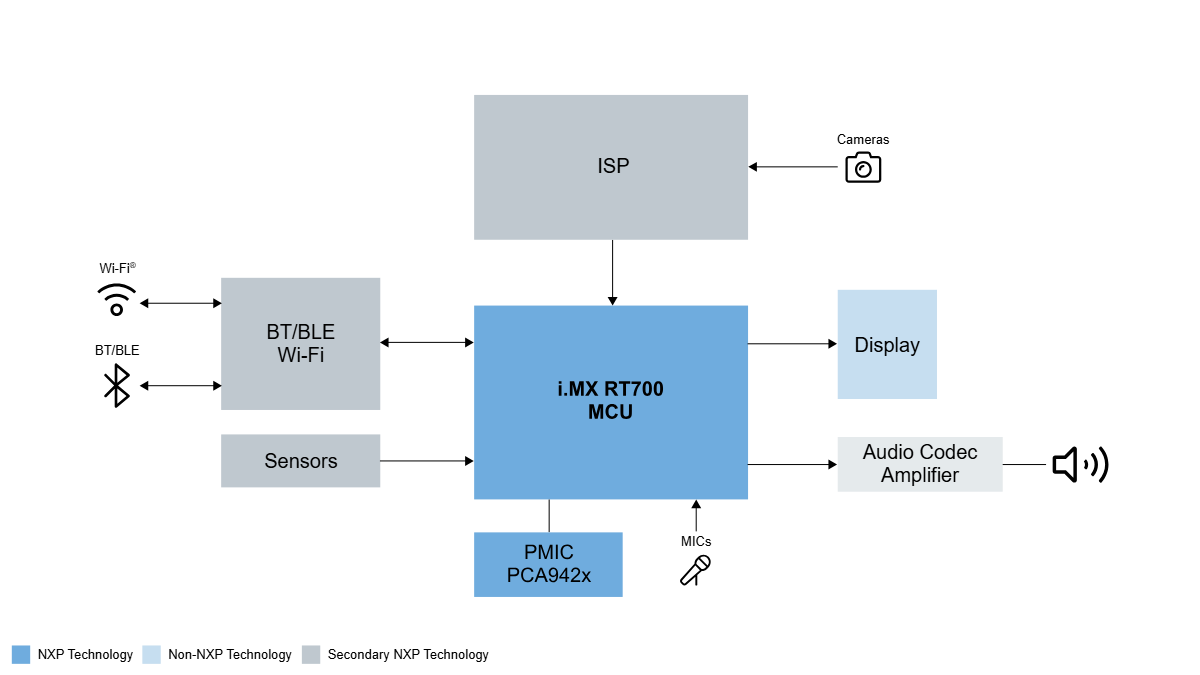
“MCU-only” Architecture
The “MCU-only” solution opens the door to designs with longer battery life, lighter and smaller frames, giving OEMs an easier path towards user comfort. With weight being one of the most important factors in the user experience of glasses, the MCU-only architecture reduces the number of components as well as the size of the battery. The weight of the glasses can be brought down to within 30g.
The strategy of an MCU-only architecture puts more emphasis on the microcontroller’s features and capabilities. Many features of the AP-Coprocessor design are expected within the MCU design. It is therefore critical to include features such as NPU, DSP, and a high-performing CPU core.
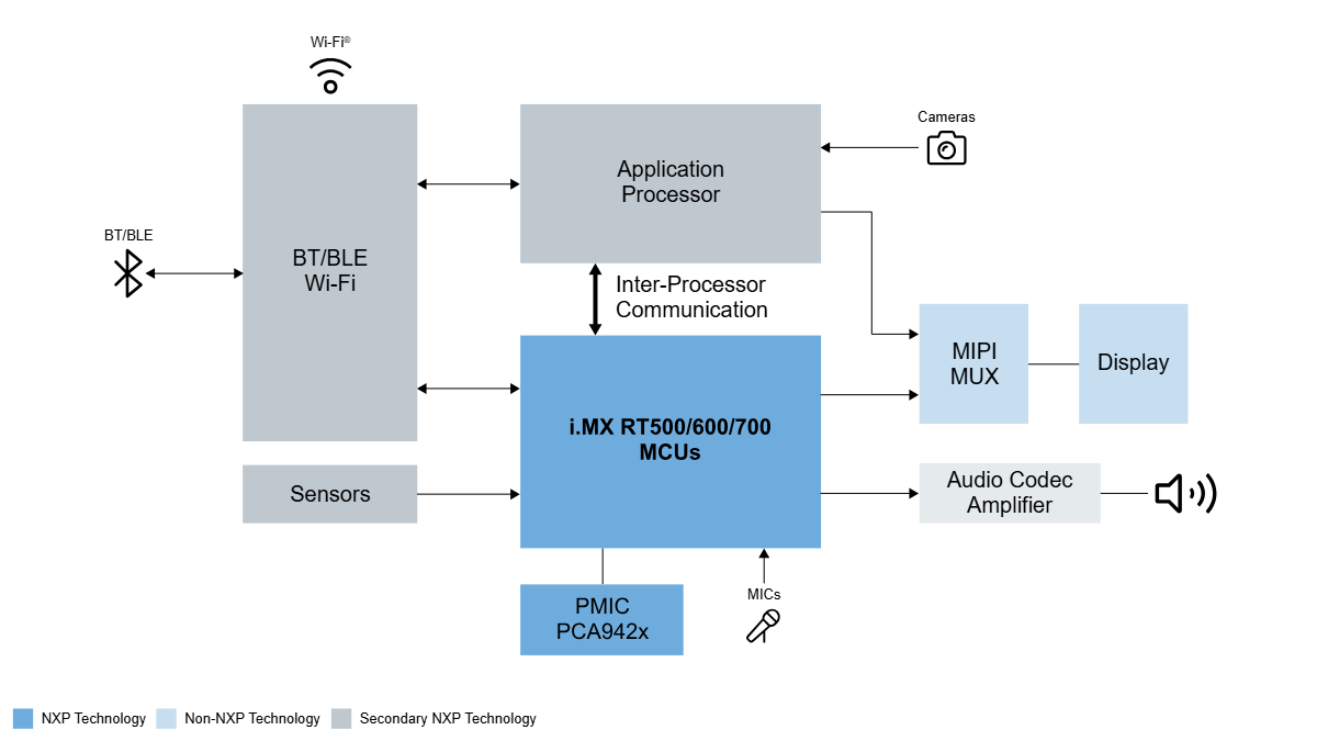
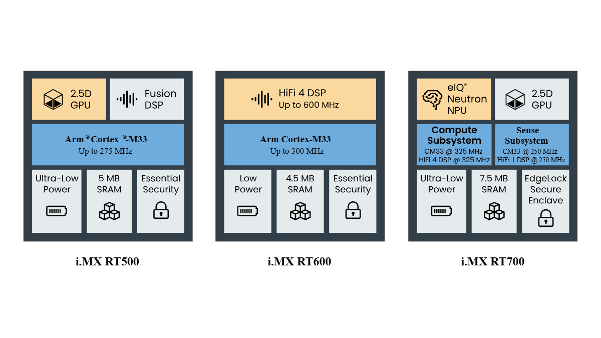
NXP’s Solution: The i.MX RT Family as the Ideal Coprocessor
The i.MX RT500, i.MX RT600 and i.MX RT700 has three chips in NXP’s i. MX RT low-power product family. These chips, as coprocessors, are currently widely used in the latest AI eyewear designs for many customers around the world. The i.MX RT500 Fusion F1 DSP can support voice wake-up, music playback, and call functions of smart glasses. The i.MX RT600 is mainly used as an audio coprocessor for smart glasses, supporting most noise reduction, beamforming, and wake-up algorithms. The i.MX RT700 features dual DSP (HiFi4/HiFi1) architecture and supports algorithmic processing of multiple complexities, while enabling greater power savings with the separation of power/clock domains between compute and sense subsystems.
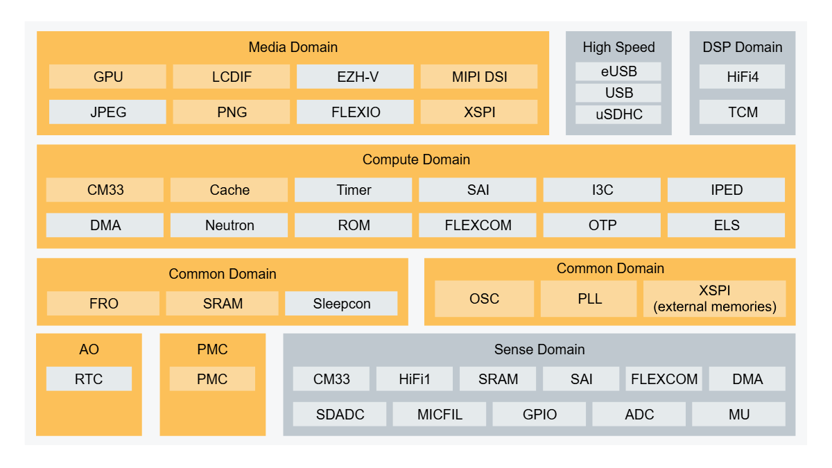
How the i.MX RT700 Maximises Battery Life
As a coprocessor in AI glasses, the i.MX RT700 can flexibly configure power management and clock domains to switch roles based on different application scenarios: it can be used as an AI computing unit for high-performance multimedia data processing, and it can also be used as a voice input sensor hub for data processing in ultra-low power consumption.
AI glasses mainly rely on voice control to achieve user interaction, so voice wake-up is the most commonly used scenario and the key to determining the battery life of AI glasses. In mainstream use cases, the coprocessor remains in active mode at the lowest possible core voltage levels, awaiting the user’s voice commands, quickly switching to speech recognition mode with noise reduction in potentially noisy environments. Based on this user scenario, the i.MX RT700 can be configured to operate in sensor mode; at this time, only a few modules, such as HiFi1 DSP, DMA, MICFIL, SRAM, and power control (PMC), are active. The Digital Audio Interface (MICFIL) allows microphone signal acquisition; DMA is used for microphone signal handling; HiFi1 is used for noise reduction and wake-up algorithm execution, while the compute domain is in a power-down state.
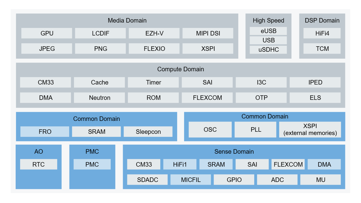
Other low-power technologies included in the RT700, such as distortion-free audio clock source FRO, microphone module FIFO, and hardware voice detection (Hardware VAD), DMA wake-up also ensures that the system power consumption of i.MX RT700 voice wake-up scene can be under 2 mW, maximising power consumption while continuously monitoring.
RT700 also powers MCU-only
For display-related user scenarios, the i.MX RT700 can be configured in “High Performance Mode”, where the Vector Graphics Accelerator (2.5D GPU), Display Controller (LCDIF), and Display Bus (MIPI DSI) are enabled. While enabling high performance, the compute domain also takes advantage of low-power technologies such as MIPI ULPS (Ultra Low Power State), dynamic voltage regulation within the Process Voltage Temperature (PVT) tuning, and other low-power technologies.
With the continuous integration of intelligent hardware and artificial intelligence, choosing the right low-power high-performance chip has become the key to product innovation. With its deep technology accumulation, the i.MX RT series provides a solid foundation for cutting-edge applications such as AI glasses.
The post AI Glasses: Ushering in the Next Generation of Advanced Wearable Technology appeared first on ELE Times.
The semiconductor technology shaping the autonomous driving experience
Courtesy: Texas Instruments
Last summer in Italy, I held my breath as I prepared to drive down a narrow cobblestone road. It was pouring rain with no sign of stopping, and I could hardly see. Still, I pressed the gas pedal, my shoulders tense and my hands gripping the wheel.
This is just one example of a stressful driving experience. Whether it’s enduring a long road trip or crawling through bumper-to-bumper traffic, many people find driving to be nerve-wracking. Though we can spend weeks finding the perfect car, deliberating which seats will feel the most comfortable or which stereo system will sound the richest, it’s hard to enjoy the ride when you are constantly scanning for hazards, adjusting to changing weather conditions, or navigating unknown roadways.
But what if you could appreciate the experience of being in your vehicle while trusting your car to navigate the stressful drives for you?
We’re progressing toward that future, with worldwide investment in autonomous vehicles expected to grow by over US$700 million in 2028. But to understand the vehicle of the future, we must first understand how its architecture is evolving.
How software-defined vehicles (SDVs) are transforming automotive architecture
I can’t discuss the vehicle of the future without starting with the transition to software-defined vehicles (SDVs). Because SDVs have radar, lidar, and camera modules, they are critical to a future where drivers have the latest automated driving features without having to purchase a new vehicle every few years.
For automotive designers, SDVs require separating software development from the hardware, fundamentally changing the way that they build a car. When carmakers consolidate software into fewer electronic control units (ECUs), they can make their vehicle platforms more scalable and streamline over-the-air updates. These ECUs can handle the control of specific autonomous functions in real time, such as automatic braking or self-steering modules.
How integrated sensor fusion enables higher levels of vehicle autonomy
When SDVs centralise software, they’re capable of integrating advanced driver assistance system technologies that enable increased levels of vehicle autonomy. On today’s roads, using the Society of Automotive Engineers’ Levels of Driving Automation, level 1 or 2 (which requires people to drive even when support features are engaged) is the most prevalent. But what about in the future?
I envision that one day, every car will have accurate level 3 or 4 autonomy, characterised by automated driving features that can operate a vehicle under specific conditions. The advances in technology happening now will enable drivers to trust features in future vehicles as much as features like cruise control today. Instead of being fully responsible for stressful driving tasks, we can trust the vehicle’s system to take the lead. And at the heart of this evolution are semiconductors.

To achieve higher levels of vehicle autonomy, the ability to accurately detect and classify objects and respond in real time will require more advanced sensing technologies. The concept of combining data from multiple sensors to capture a comprehensive image of a vehicle’s surroundings is called sensor fusion. For example, if a radar sensor classifies an object as a tree, a second technology, such as lidar or camera, can confirm it in order to communicate to the driver that the tree is 50 feet ahead, enabling swift action.
Why future vehicles need a high-speed, Ethernet-based data backbone
I like to say that tomorrow’s cars are like data centres on wheels, processing multiple large streams of high-speed data seamlessly.
The car’s computer, among other functions, coordinates things such as radar, audio, and data transfer in a high-speed communication network around the vehicle. While legacy communication interfaces for in-vehicle networking, such as Controller Area Network (CAN) and Local Interconnect Network (LIN), remain essential for controlling fundamental vehicle applications such as doors and windows, these interfaces must seamlessly integrate with emerging technologies. In order to accommodate the higher data processing needs of new vehicles, Ethernet will be the prevailing technology. Automotive Ethernet has emerged as a “digital backbone” to efficiently manage applications ranging from audio to standard radar.
As vehicles become capable of higher levels of autonomy, automotive designers will need higher-bandwidth networks for applications including high-resolution video and streaming radar. At TI, our portfolio supports diverse functions with varying requirements, readying us for that network evolution. With technologies like FPD-Link, vehicles can stream uncompressed, high-bandwidth radar, camera, and lidar data to the central compute to respond to events in real-time.
Design engineers must also have a powerful processor in the central computing system that can take data from multiple technologies, such as lidar, camera, and radar sensors, to complete a fast, real-time analysis and provide a 4D data breakdown to better perform object classification.
With expertise in radar, Ethernet, FPD-Link technology and central compute, TI works with automotive designers to help optimise solutions from end to end. Rather than designing devices that only perform one function, we look at how to best optimise our device ecosystem. For example, we design radar devices that easily interface with our Jacinto processors to achieve faster, more accurate decision-making.
What these advancements mean for the future driving experience
In the future, if I encounter the same road and rainy conditions in Italy as I did this summer, I might not drive. Instead, I might trust my car to safely get me to my destination, while I relax in my seat.
The vehicle of the future might not exist yet. But the technologies we’re developing today are making the vehicle of the future – and maybe even the next breakthrough of the future – real.
The post The semiconductor technology shaping the autonomous driving experience appeared first on ELE Times.
The electronics Industry in 2026 and Beyond: A Strategic Crossroads
As we stand on the threshold of 2026, the global electronics industry is undergoing a profound transformation. It is now a linchpin of industrial, strategic, and geopolitical competition, with implications for economies, national security, and everyday life. In a world where electronic systems power everything from personal communication to national infrastructure, the industry’s trajectory through 2026 and beyond will be a trendsetter for economic competitiveness and technological leadership worldwide.
Worldwide, electronic systems and semiconductor markets have regained strong growth momentum following recent supply fluctuations and trade tensions. In major economies, consumer-facing electronics still matter – smart TVs, connected appliances and IoT devices feature prominently in growth forecasts – but industrial and strategic demand is shaping the industry’s future. AI acceleration, 5G/6G networks, edge computing and automated factories are expanding the role of electronics far beyond personal use into the backbone of tomorrow’s digital economy.
For emerging economies like India, 2026 marks a pivotal year. Once predominantly an assembly hub, India’s electronics landscape is evolving quickly toward manufacturing depth and export competitiveness. Under initiatives like Make in India and Production-Linked Incentive schemes, India is targeting an ambitious USD 300 billion in domestic electronics production by 2026.
Despite progress in finished products, the industry’s most strategic component – the semiconductor – remains the ultimate litmus test of technological sovereignty. Demand for advanced logic, memory and power chips continues to skyrocket as AI, data centres, autonomous systems and EVs proliferate. However, high-end semiconductor fabrication is concentrated in a few global hubs, creating political and economic frictions. Expansion efforts are underway; India aims to bring complex chip manufacturing and packaging closer to local markets.
Now the industry’s evolution will hinge on architectural and material innovation as much as volume growth. Emerging manufacturing techniques like 3D-printed electronics, wide-band-gap power devices (such as GaN and SiC), and advanced packaging are reshaping how electronic systems are built and what they can do.
Integration with AI and machine learning at the edge – beyond centralised cloud systems – is transforming everything from consumer devices to industrial controls. AI-powered industrial machines, smart wearables and edge computing systems are now central to innovation narratives that go far beyond smartphones and laptops.
Governments play a deciding role in semiconductor incentives, R&D investment, and skills ecosystem development. India’s push into electronics manufacturing underscores how policy can unlock domestic value addition and attract foreign direct investment.
A young workforce is being credited with driving innovation in design labs and new technology ventures. This demographic shift could help transcend low-value assembly toward high-value engineering and R&D.
By the end of the decade, the core electronics industry will be defined by: reducing reliance on limited geographic hubs for chips and components; hardware designed for AI workloads will proliferate; energy efficiency and green manufacturing will be essential competitive factors, and new alliances and regional clusters will diversify global supply chains.
Let us check a few facts about a comprehensive, forward-looking overview of India’s electronics industry – where it stands now, the key forces shaping its future, and what lies ahead in the coming decade. India’s electronics production rose from Rs. 1.9 lakh crore in 2014–15 to Rs. 11.3 lakh crore in FY 2024–25 – a six-fold jump in a decade. Exports have similarly surged eightfold in that period.
Production Linked Incentive schemes significantly boost manufacturing across mobile phones, IT hardware, and components. The Electronics Components Manufacturing Scheme offers capital subsidies to build domestic production of PCBs and critical parts. The Scheme for Promotion of Manufacturing of Electronic Components and Semiconductors supports capital expenditure for high-value component plants. These policies aim to reduce dependence on imports, attract foreign investors, and expand high-value manufacturing. The global supply-chain shift, e.g., China + 1 strategies, is prompting electronics makers to diversify production to India. States like Uttar Pradesh, Tamil Nadu, Karnataka, and Andhra Pradesh are becoming hubs for manufacturing and exports — bringing infrastructure and investment.
There are certain challenges that India must overcome. It includes Component Import Dependency – despite growth in assembly, 85–90 % of electronics component value is still imported, especially from China, Korea, and Taiwan. Building domestic supply chains for PCBs, semiconductors, connectors, and precision parts remains a major hurdle. Bureaucratic delays in certifications are slowing production schedules and product launches. Production costs in India can be 10–20 % higher than in other Asian hubs, and R&D infrastructure for high-end semiconductors is still limited. India needs deep innovation capacity – not just assembly, but to move up the value chain.
India has set a target for itself for the coming years, such as a target of up to USD 500 billion in electronics manufacturing output by 2030. Achieving this would require scaling capacity, improving infrastructure, and drawing more global players into deeper parts of the supply chain. India needs to broaden Electronics Ecosystem Growth – Automotive electronics, industrial IoT, wearables/AI devices, and telecom equipment to expand domestic and export markets. EMS output is projected to grow rapidly, potentially capturing a larger share of the global EMS market. Semiconductor Ecosystem Development – policies are moving into a “scale-up phase” to build design, assembly, and, over time, manufacturing capabilities – crucial for tech sovereignty and global relevance. Global shifts in supply chain diversification present opportunities for India to attract investments that might otherwise be concentrated in China or Southeast Asia.
Geopolitical-economic dynamics are a significant stumbling block for India’s electronics industry, especially in relation to China and the United States – but it’s also both a challenge and an opportunity.
India’s electronics manufacturing growth has been strongly influenced by global tensions between China and the U.S. After the pandemic and during the U.S.-China trade/tech war, global supply chains began diversifying away from China – a “China +1” effect – and India benefited from this shift as multinational firms looked for alternatives for parts of their production.
Despite India’s assembly growth in mobile phones and other electronics, the industry remains heavily reliant on Chinese imports for key components and machinery. This dependency means that geopolitical friction with China can slow production, raise costs, and create supply bottlenecks for Indian electronics makers.
U.S.-India trade Frictions are also impacting growth. The U.S. imposed a high tariff of up to 50 % on Indian goods, which affects overall trade dynamics that make it harder for Indian electronics producers to scale exports cost-effectively. Hence, India is caught in a complex geopolitical squeeze: China remains essential for many inputs but is a strategic rival, while the U.S. provides market and technology ties but has also used tariffs as leverage.
On the other hand, India’s electronics exports to the U.S. had raced ahead by leveraging trade tensions that kept Chinese goods less competitive. But the recent reduction of U.S.–China tariffs has reduced India’s cost edge by around 10 percentage points, threatening export growth and investment momentum in the sector. India’s industry competitiveness isn’t purely industrial – it’s shaped by geopolitical policy decisions in Washington and Beijing.
Nevertheless, India’s electronics industry is poised for one of the most transformative growth phases in its history. With supportive policy frameworks, rising global demand, and strategic investments in talent and infrastructure, India could evolve from a largely assembly-focused hub to a comprehensive electronics and semiconductor powerhouse over the next decade – if it successfully strengthens its component base, resolves regulatory bottlenecks, and nurtures innovation ecosystems.
Devendra Kumar
Editor
The post The electronics Industry in 2026 and Beyond: A Strategic Crossroads appeared first on ELE Times.
Keysight & Samsung: Industry-First NR-NTN S-Band & Satellite Mobility Success
Keysight Technologies announced a groundbreaking end-to-end live new radio non-terrestrial networks (NR-NTN) connection in band n252, as defined by the Third Generation Partnership Project (3GPP) under Release 19, achieved using Samsung Electronics’ next-generation modem chipset. The demonstration, taking place at CES 2026, includes live satellite-to-satellite (SAT-to-SAT) mobility using commercial-grade modem silicon and cross-vendor interoperability, marking an important milestone for the emerging direct-to-cell satellite market.
The achievement also represents the public validation of n252 in an NTN system, a new band expected to be adopted by next-generation low Earth orbit (LEO) constellations.
Reliable global connectivity is a growing requirement for consumers, vehicles, IoT devices, and critical communications. As operators, device manufacturers, and satellite providers accelerate investment in NTN technologies, this achievement shows decisive progress toward direct-to-cell satellite coverage.
With the addition of n252 alongside earlier NTN demonstrations in n255 and n256, all major NR-NTN FR1 bands have now been validated end-to-end. This consolidation of band coverage is critical for enabling modem vendors, satellite operators, and device manufacturers to evaluate cross-band performance and mobility holistically as they prepare for commercial NTN services.
Keysight’s NTN Network Emulator Solutions recreate realistic multi-orbit LEO conditions, SAT-to-SAT mobility, and end-to-end routing while running live user applications over the NTN link. Together with Samsung’s chipset, the system validates user performance, interoperability, and standards conformance, providing a high-fidelity test environment that reduces risk, accelerates trials, and shortens time-to-market for NR-NTN solutions expected to scale in 2026.
The demonstration integrates Samsung’s next-generation modem chipset with Keysight’s NTN emulation portfolio to deliver real, standards-based NTN connectivity across a complete system. The setup validates end-to-end link performance, mobility between satellites, and multi-vendor interoperability, essential requirements for large-scale NTN deployments.
Peng Cao, Vice President and General Manager of Keysight’s Wireless Test Group, Keysight, said: “Together with Samsung’s System LSI Business, we are demonstrating the live NTN connection in 3GPP band n252 using commercial-grade modem silicon with true SAT-to-SAT mobility. With n252, n255, and n256 now validated across NTN, the ecosystem is clearly accelerating toward bringing direct-to-cell satellite connectivity to mass-market devices. Keysight’s NTN emulation environment enables chipset and device makers a controlled way to prove multi-satellite mobility, interoperability, and user-level performance, helping the industry move from concept to commercialisation.”
The post Keysight & Samsung: Industry-First NR-NTN S-Band & Satellite Mobility Success appeared first on ELE Times.
Quantum Technology 2.0: Road to Transformation
Courtesy: Rhode & Schwarz
After more than 100 years of research, quantum technology is increasingly finding its way into everyday life. Examples include its use in cell phones, computers, medical imaging methods and automotive navigation systems. But that’s just the beginning. Over the next few years, investment will increase significantly, and lots of other applications will take the world by storm. While test & measurement equipment from Rohde & Schwarz and Zurich Instruments is helping develop these applications, the technology group’s encryption solutions are ensuring more secure communications based on quantum principles.
Expectations for quantum technology are greater than in almost any other field. That’s no surprise, given the financial implications associated with the technology. For example, consulting firm McKinsey & Company estimates the global quantum technology market could be worth 97 billion dollars by 2035. According to McKinsey, quantum computing alone could be worth 72 billion dollars, and quantum communications up to 15 billion.
Previous developments clearly show that the projected values are entirely realistic. Many quantum effects have become part of our everyday lives. Modern smartphones, for example, contain several billion transistors, predominantly in flash memory chips. Their function – controlling currents and voltages – is based on the quantum mechanical properties of semiconductors. Even the GPS signals used in navigation systems and the LEDs used in smartphone flashlights are based on findings from quantum research.
To celebrate these achievements, UNESCO declared 2025 the “International Year of Quantum Science and Technology” – exactly 100 years after German physicist Werner Heisenberg developed his quantum mechanics theory based on the research findings of the time. Quantum technology was also in the spotlight with the 2025 Nobel Prize in Physics, which was awarded to quantum researchers John Clarke, Michel Devoret, and John Martinis.
Quantum technology 2.0: what can we expect?Quantum physics in secure communications: Whether personal or professional, beach holiday snapshots or development proposals for new products, our data and data transmission need to be protected. Companies today consistently name cyberattacks and the resulting consequences as the top risk to their business. Developments in quantum computing are revealing the limits of conventional encryption technologies. Innovations in quantum communications are the key to the future, as they enable reliable detection of unauthorised access. This means you can create a genuine high-security channel for sensitive data.
Upgrading supply chains: Global flows of goods reach every corner of the Earth, and everything is now just a click away: a new tablet for home use or giveaways for a company party. But behind the scenes lies a complex logistics network of manufacturers, service providers, suppliers, merchants, shipping companies, courier services, and much more. The slightest backlog at a container port or change in the price of purchased items means alternatives must be found – preferably in real time. But the complexity of this task is also beyond what conventional computers can handle.
Personalised medicine: Everyone is different, and so are our illnesses. Cancer cells, for example, differ from one person to the next and often change over time. These differences and changes are already well documented in analytical terms, which has created huge amounts of data. Big Data is the buzzword. But evaluating this data quickly and effectively, to develop personalised forms of treatment, is impossible for conventional computers.
Fast. Faster. Quantum computing.
Our world is controlled by binary code. Conventional computers process data as sequences of ones and zeros, true or false, off or on. This applies to everything, from simple text processing to virtual reality in the metaverse. But the world we live and work in is becoming increasingly complex. The amount of data we need to process is growing rapidly. In 2024, global digital data traffic had more than quadrupled over the space of just five years to 173.4 zettabytes. By 2029, experts believe this number will reach 527.5 zettabytes, equivalent to 527.5 trillion gigabytes.
Conventional computers face two insurmountable obstacles as a result: time and complexity. The larger the volume of data, the more time you need to process that data sequentially. The more complex the problem, the lower the probability that a binary code, with only two states, will be able to efficiently calculate a solution. Quantum computers have the potential to overcome both obstacles using insights from modern physics.
Hand in hand instead of either-or
Like conventional bits, quantum bits (qubits) form quantum mechanical memory units. In addition to just zeros and ones, they can also assume overlapping, mixed states. This simultaneity represents a fundamental technological paradigm shift. We can now run conventional sequential calculation methods simultaneously, which is why a quantum computer can save so much time.
But above all, the new quantum mechanical approach allows us to process new and much more complex questions. However, it’s not an either-or decision, either conventional processing power or quantum computing. Instead, what matters is integrating existing and quantum systems depending on the task.
Physics versus logic
In the quantum world, a particle can be in two places at the same time. Only when it is observed can you narrow down its location, for example, by measuring it. This unusual property is also why it is extremely unstable. Instead of using individual physical qubits, which can be very error-prone, multiple qubits are grouped into a logical qubit. However, the challenge here is that you need quantum systems with as many as one million logical qubits in order to answer practical questions, like protein folding. A logical qubit can contain up to 100 physical qubits, but the highest processing capacity is currently only 1,225 physical qubits.
Zurich Instruments has been part of the Rohde & Schwarz family since 2021. The T&M market for quantum computing holds enormous potential for both companies. Operating and maintaining quantum computers requires a wide range of specific T&M solutions because RF signals need to be generated and measured with extremely high precision to effectively create and record quantum states. Control systems for quantum computers are part of the company’s portfolio.
Secure. More secure. Quantum communications
Quantum computers have the potential to push the limits of processing efficiency. But this brings challenges, including secure communications – increasingly a priority in view of “Q-Day”, the point at which quantum computers will be able to crack classic encryption.
That is why alternative encryption methods are becoming increasingly important. There are essentially two main approaches. The first is post-quantum cryptography, which involves conventional encryption methods with one key difference: they can survive attacks from quantum computers unscathed. The algorithms used in this approach are based on theoretical assumptions for which no effective attacks are currently known using either quantum or conventional computers.
The other approach relates to quantum key distribution (QKD). The German Federal Office for Information Security (BSI) and the National Institute of Standards and Technology (NIST) are two of the main drivers of innovation in this area. In an increasingly digitalised world, private-sector customers, and government customers in particular, are dependent on trustworthy IT security solutions. Secure communications networks have become a critical infrastructure in advanced information societies.
These innovative solutions are shifting the focus of cryptology. Conventional methods, as well as more recent post-quantum methods, are based on mathematical assumptions, i.e. the idea that certain tasks cannot be calculated with sufficient efficiency. Quantum key distribution, by contrast, is based on physical principles. Rohde & Schwarz Cybersecurity is providing and leveraging its extensive expertise in security solutions, as well as its experience in building and implementing secure devices and systems, in a variety of research projects.
The post Quantum Technology 2.0: Road to Transformation appeared first on ELE Times.
Develop Highly Efficient X-in-1 Integrated Systems for EVs
Courtesy: Renesas
The recent tightening of CO2 emission regulations has accelerated the electrification of automobiles at an unprecedented pace. With the global shift from hybrid vehicles to electric vehicles (EVs), automakers are demanding more efficient, safe, and reliable systems. System integration, known as “X-in-1”, becomes the focus of attention. This innovative concept integrates functions traditionally controlled by separate MCUs, such as inverters, onboard chargers (OBC), DC/DC converters, and battery management systems (BMS), into a single microcontroller (MCU), achieving simultaneous miniaturisation, cost reduction, and efficiency improvement. As electric vehicles evolve, demand grows for X-in-1 configurations that consolidate multiple applications onto a single MCU.
At the core of this X-in-1 approach is Renesas’ RH850/U2B MCUs. This next generation of MCUs delivers the advanced control, safety, and security required by EVs on a single chip. It features a high-performance CPU with up to six cores, operating at up to 400MHz, enabling both real-time control and parallel processing. It also offers comprehensive analogue and timer functions for inverter and power converter applications, enabling efficient control of the entire electrification system on a single chip. Furthermore, the RH850/U2B MCUs offer a wide memory lineup, allowing flexible implementation of the optimal X-in-1 system tailored to specific requirements.
 Figure 1. Comparison of MCU Configuration Before and After X-in-1 Integration
The RH850/U2B MCU demonstrates overwhelming superiority in inverter control, maximising the driving performance of EVs. With dedicated hardware optimised for inverter control, including a resolver-to-digital converter (RDC), an analogue-to-digital converter (ADC), and timers for three-phase motors, the RH850/U2B MCU enables high-speed, high-precision control at the hardware level that software alone cannot achieve. The integrated RDC eliminates the need for external angle detection ICs, contributing to reduced component count and simplified board design. Furthermore, the embedded Renesas proprietary Enhanced Motor Control Unit (EMU) executes complex control calculations in the hardware, significantly reducing CPU load while achieving high-speed, high-precision motor control (EMU is only included in the RH850/U2B6).
 Figure 2. Comparison of External RDC and Internal RDC
The next-generation power devices using silicon carbide (SiC) and gallium nitride (GaN) are increasingly being adopted in OBCs and DC/DC converters. These devices enable high efficiency and fast switching, directly contributing to shorter charging times and improved energy efficiency. On the other hand, the RH850/U2B MCU incorporates a multifunctional timer (generic timer module (GTM)*2 and high-resolution PWM) that is capable of generating high-speed, high-resolution waveforms (minimum resolution of 156.25ps). This facilitates control that leverages the high-speed switching characteristics of SiC and GaN. It also incorporates a 12-bit fast comparator for high-frequency switching control and protection operations.
In addition to speed and energy efficiency, the RH850/U2B MCU also delivers outstanding performance in battery management systems, the heart of EVs. Monitoring and controlling the voltage and temperature of hundreds of cells demands high processing power. The RH850/U2B MCU features a multi-core CPU, allowing surplus resources to be allocated to BMS processing. This enables system miniaturisation and cost reduction without requiring additional MCUs.
As EVs proliferate, the importance of safety and security becomes critical. Compliant with ISO 26262 ASIL D, the RH850/U2B MCU ensures functional safety at the hardware level. It also incorporates security features compliant with EVITA Full, enabling the construction of highly secure systems even in X-in-1 configurations.
The evolution of EVs is moving towards faster, safer, and more efficient use of automobiles. Achieving this requires meeting new demands that conventional MCUs cannot fully address. The RH850/U2B MCU enables users to meet the needs of EVs with high-speed, high-precision inverter control via dedicated hardware; highly efficient switching control in OBCs and DC/DC converters using high-resolution, high-speed timers; multi-core utilisation in battery management systems; and comprehensive safety and security support.
The post Develop Highly Efficient X-in-1 Integrated Systems for EVs appeared first on ELE Times.
Pages

