
ELE Times

Breakthrough in D-band Wireless: Anritsu and VTT Demonstrate World-Leading Transmit array-Based High-Speed Connectivity
Anritsu and VTT Technical Research Centre of Finland have demonstrated a major advance in D-band wireless communications by validating a beam-steering transmit array antenna system using advanced test equipment. The achievement confirms the feasibility of stable, high-capacity wireless links for next-generation backhaul, industrial, defence and future 6G networks.
Using Anritsu’s precision test equipment and VTT’s steerable transmitarray antenna, the teams achieved high-speed wireless links across the 110–170 GHz D-band. Link performance and beam-steering behaviour were assessed under realistic over-the-air (OTA) conditions using wideband modulated signals up to 8 GHz bandwidth. This system-level characterisation, from signal generation to OTA performance, confirmed multi-gigabit data rates in the tens-of-Gbps range, including 20 Gbps over 1 m and reliable operation up to 7 m, setting a new benchmark for D-band connectivity.
The demonstration features a lightweight, scalable transmitarray antenna developed by VTT, incorporating advanced phase-shifting elements and vector-modulator MMICs. Its electronically steerable design provides rapid, precise beam control without mechanical movement, maintaining signal strength under changing conditions. Supported by Anritsu’s state-of-the-art test equipment, the results reflect a proven, instrumentation-grade measurement approach that ensures reliability and scalability for future deployments.
“Anritsu is proud to collaborate with VTT to advance the practical use of D-band wireless technology. Together, we have validated performance levels that bring high-frequency wireless links closer to real-world deployment,” said Jonathan Borrill, CTO, Test & Measurement, Anritsu.
“This milestone shows how strategic partnerships turn deep tech into a competitive advantage. By combining VTT’s steerable transmitarray expertise with Anritsu’s precise instrumentation‑grade validation, we shorten adoption cycles and scale D‑band from the lab to live networks — creating growth opportunities across critical infrastructure, manufacturing, defence, 6G and beyond,” said Tauno Vähä‑Heikkilä, Director, Strategic Partnerships, VTT.
Anritsu and VTT will now engage with industry partners to evaluate use cases and prepare the technology for upcoming field trials and deployments, marking a landmark step toward realising the potential of D-band wireless for next-generation networks.
The post Breakthrough in D-band Wireless: Anritsu and VTT Demonstrate World-Leading Transmit array-Based High-Speed Connectivity appeared first on ELE Times.
Redefining Edge Computing: How the STM32V8 18nm Node Outperforms Legacy 40nm MCUs
STMicroelectronics held a virtual media briefing, hosted by Patrick Aidoune, General Manager, General Purpose MCU Division at ST, on November 17, 2025. The briefing was held before their flagship event, the STM32 Summit, where they launched STM32V8, a new generation of STM32 microcontrollers.
STMicroelectronics introduced its new generation microcontroller, STM32V8, under the STM32 class recently. Built on an innovative 18nm process technology with FD-SOI and phase change memory (PCM) technology included, this microcontroller is the first of its kind in the world. It is the first under 20nm process to use FD-SOI along with an embedded PCM technology.
FD-SOI Technology
The FD-SOI is a silicon technology, co-developed by ST, which brought innovation in the aerospace and automotive applications. The 18nm process, co-developed with the Samsung Foundry, provides a cost-competitive leap in both performance as well as power consumption.
The FD-SOI technology gives a strong robustness to ionising particles and reliability in harsh operating environments, which makes it particularly suitable for intense radiation exposure found in earth orbit systems. The FD-SOI also helps reduce the static power consumption, along with allowing operations on a lower voltage supply, while sustaining harsh industrial environments as well.
Key Features
STM32V8’s Arm Cortex-M85 core, along with the 18nm process, gives it a clock speed of up to 800MHz, making it the most powerful STM32 ever shipped. It has also been embedded with up to 4 Mbytes of user memory in a competitive dual bank, allowing bank swapping for seamless code updates.
Keeping in mind the needs of developers, the STM32V8 provides for more compute headroom, along with more security and improved efficiency. Compared it is 40nm process node with the same technologies, the STM32V8 brings with it improved performance, higher density, and better power efficiency.
Industrial Applications
This new microcontroller is a multipurpose system to benefit several industries:
- Factory Automation and Robotics
- Audio Applications
- Smart Cities and Buildings
- Energy Management Systems
- Healthcare and Biosensing
- Transportation (ebikes)
Achievements
ST’s new microcontroller has been selected by SpaceX for its high-speed connectivity system in the Starlink Satellite System.
“The successful deployment of the Starlink mini laser system in space, which uses ST’s STM32V8 microcontroller, marks a significant milestone in advancing high-speed connectivity across the Starlink network. The STM32V8’s high computing performance and integration of large embedded memory and digital features were critical in meeting our demanding real-time processing requirements, while providing a higher level of reliability and robustness to the Low Earth Orbit environment, thanks to the 18nm FD-SOI technology. We look forward to integrating the STM32V8 into other products and leveraging its capabilities for next-generation advanced applications,” said Michael Nicolls, Vice President, Starlink Engineering at SpaceX.
STM32V8, like its predecessors, is expected to draw significant benefit from ST’s edge AI ecosystem, which is under continued expansion. Currently, the STM32V8 is in early-stage access for selected customers with key OEMs’ availability as of the first quarter 2026 and with broader availability to follow.
Apart from unveiling the new generation microcontroller, ST also announced the expansion of its STM32 AI Model Zoo, which is part of the comprehensive ST Edge AI Suite of tools. The STM32 AI Model Zoo has more than 140 models from 60 model families for vision, audio, and sensing AI applications at the edge, making it the largest MCU-optimised library of its kind.
This AI Model Zoo has been designed, keeping in mind the requirements of both data scientists and embedded systems engineers, a model that’s accurate enough to be useful and that also fits within their energy and memory constraints.
The STM32 AI Model Zoo is the richest in the industry, for it not only offers multiple models, but also scripts to easily retrain models, evaluate accuracy, and deploy on boards. ST has also introduced native support for PyTorch models. This complements their existing support for TensorFlow, Keras AI frameworks, LiteRT, and ONNX formats, giving developers additional flexibility in their development workflow. They are also introducing more than 30 new families of models, which can use the same deployment pipeline. Many of these models have already been quantised and pruned, meaning that they offer significant memory size and inference time optimisations while preserving accuracy.
Additionally, they also announced the release of STM32 Sidekick, their new AI agent on the ST Community, available 24/7. This new AI agent is trained on official STM32 documentation (datasheets, reference manuals, user manuals, application notes, wiki entries, and community knowledge base articles) to help users locate relevant technical data, obtain concise summaries of complex topics, and discover insights and documents. Alongside, they announced STM32WL3R, a version of their STM32WL3 tailored for remote control applications supporting the 315 MHz band. The STM32WL3R is a sub-GHz wireless microcontroller with an ultra-low-power radio.
~ Shreya Bansal, Sub-Editor
The post Redefining Edge Computing: How the STM32V8 18nm Node Outperforms Legacy 40nm MCUs appeared first on ELE Times.
“‘Bharat’ will become a major player in entire electronics stack…”, Predicts Union Minister, Ashwini Vaishnaw
Union Electronics and IT Minister Ashwini Vaishnaw predicted that ‘Bharat’ will become a major player in the entire electronics stack, in terms of design, manufacturing, operating system, applications, materials, and equipment.
In an X post, the Union Minister drew attention to a major milestone for Prime Minister Narendra Modi’s ‘Make in India’ initiative and making India a major producer economy since Apple shipped $50 billion worth of mobile phones in 2025.
“Electronics production has increased six times in the last 11 years. And electronics exports have grown 8 times under PM Modi’s focused leadership. This progress has propelled electronics products among the top three exported items,” Vaishnaw noted.
He further informed that 46 component manufacturing projects, laptop, server, and hearable manufacturers had added to the ecosystem, which are making electronics manufacturing a major driver of the manufacturing economy.
“Four semiconductor plants will start commercial production this year. Total jobs in electronics manufacturing are now 25 lakh, with many factories employing more than 5,000 employees in a single location. Some plants employ as many as 40,000 employees in a single location,” the minister informed, adding that “this is just the beginning”.
Last week, the industry welcomed the approval of 22 new proposals under the third tranche of the Electronics Components Manufacturing Scheme (ECMS) by the government, saying that it marks a decisive inflexion point in India’s journey towards deep manufacturing and the creation of globally competitive Indian champions in electronics components.
With this, the total number of ECMS-approved projects rises to 46, taking cumulative approved investments to over Rs 54,500 crore. Earlier tranches saw seven projects worth Rs 5,532 crore approved on October 22 and 17 projects amounting to Rs 7,172 crore on November 17. The rapid scale-up across tranches underscores the strong industry response and the growing confidence in India’s components manufacturing vision.
According to the IT Ministry, the 22 projects approved in the third tranche are expected to generate production worth Rs 2,58,152 crore and create 33,791 direct jobs.
The post “‘Bharat’ will become a major player in entire electronics stack…”, Predicts Union Minister, Ashwini Vaishnaw appeared first on ELE Times.
NVIDIA’s Jetson T4000 for Lightweight & Stable Edge AI Unveiled by EDOM
EDOM Technology announced the introduction of the NVIDIA Jetson T4000 edge AI module, addressing the growing demand from system integrators, equipment manufacturers, and enterprise customers for balanced performance, power efficiency, and deployment flexibility. With powerful inference capability and a lightweight design, NVIDIA Jetson T4000 enables faster implementation of practical physical AI applications.
Powered by NVIDIA Blackwell architecture, NVIDIA Jetson T4000 supports Transformer Engine and Multi-Instance GPU (MIG) technologies. The module integrates a 12-core Arm Neoverse-V3AE CPU, three 25GbE network interfaces, and a wide range of I/O options, making it well-suited for low-latency, multi-sensor, and real-time computing requirements. In addition, Jetson T4000 features a third-generation programmable vision accelerator (PVA), dual encoders and decoders, and an optical flow accelerator. These dedicated hardware engines allow stable AI inference even under constrained compute and power budgets, making the platform particularly suitable for mid-range models and real-time edge applications.
For system integrators (SIs), the modular architecture of Jetson T4000, combined with NVIDIA’s mature software ecosystem, enables rapid integration of vision, sensing, and control systems. This significantly shortens development and validation cycles while improving project delivery efficiency, especially for multi-site and scalable edge AI deployments.
For equipment manufacturers, Jetson T4000’s compact form factor and low-power design allow flexible integration into a wide range of end devices, including advanced robotics, industrial equipment, smart terminals, machine vision systems, and edge controllers. These capabilities help manufacturers bring stable AI inference into products with limited space and power budgets, accelerating intelligent product upgrades.
Enterprise users can deploy Jetson T4000 across diverse scenarios such as smart factories, smart retail, security, and edge sensor data processing. By performing inference and data pre-processing at the edge, organisations can reduce system latency, lower cloud workloads, and improve overall operational efficiency—while maintaining system stability and deployment flexibility.
In robotics and automation applications, Jetson T4000 features low power consumption, high-speed I/O and a compact footprint, making it an ideal platform for small mobile robots, educational robots, and autonomous inspection systems, delivering efficient and reliable AI computing for a wide range of automation use cases.
NVIDIA Jetson product lineup spans from lightweight to high-performance modules, including Jetson T4000 and T5000, addressing diverse requirements ranging from compact edge devices and industrial control systems to higher-performance inference applications. With NVIDIA’s comprehensive AI development tools and SDKs, developers can rapidly port models, optimise inference performance, and seamlessly integrate AI capabilities into existing system architectures.
Beyond supplying Jetson T4000 modules, EDOM Technology leverages its extensive ecosystem of partners across chips, modules, system integration, and application development. Based on the specific development stages and requirements of system integrators, equipment manufacturers, and enterprise customers, EDOM provides end-to-end support—from early-stage planning and technical consulting to ecosystem enablement. By sharing ecosystem expertise and practical experience, EDOM helps both existing customers and new entrants to the edge AI domain quickly build application capabilities and deploy edge AI solutions tailored to real-world scenarios.
The post NVIDIA’s Jetson T4000 for Lightweight & Stable Edge AI Unveiled by EDOM appeared first on ELE Times.
Anritsu to Bring the Future of Electrification Testing at CES 2026
Anritsu Corporation will exhibit Battery Cycler and Emulation Test System RZ-X2-100K-HG, planned for sale in the North American market as an evaluation solution for eMobility, at CES 2026 (Consumer Electronics Show), one of the world’s largest technology exhibitions to be held in Las Vegas, USA, from January 6 to January 9, 2026.
The launch of the RZ-X2-100K-HG in the North American market represents the first step in the global expansion efforts of TAKASAGO, LTD., which holds a significant share in the domestic EV development market, and it is an important measure looking ahead to future global market growth.
At CES 2026, a concept exhibition will showcase the Power HIL evaluation system combining the RZ-X2-100K-HG with dSPACE’s HIL simulator, demonstrating a new direction for the EV evaluation process.
Additionally, the power measurement solutions from DEWETRON, which joined the Anritsu Group in October 2025, will also be exhibited. Using a three-phase motor performance evaluation demonstration, we will present example applications.
About the RZ-X2-100K-HGThe RZ-X2-100K-HG is a test system developed by TAKASAGO, LTD. of the Anritsu Group, equipped with functions for charge-discharge testing and battery emulation that support high voltage and large current. It is a model based on the RZ-X2-100K-H, which has a proven track record in Japan, adapted to comply with the United States safety standards and input power specifications. This system is expected to be used for testing the performance, durability, and safety of automotive batteries and powertrain devices in North America.
About Power HILPower HIL (Power Hardware-in-the-Loop) is an extended simulation technology that combines virtual and real elements by adding a “real power supply function” to HIL (Hardware-in-the-Loop). Power HIL creates a virtual vehicle environment with real power, reproducing EV driving tests and charging tests compatible with multiple charging standards under conditions close to reality. This allows for high-precision and efficient evaluation of battery performance, safety, and charging compatibility without using an actual vehicle.
Terminology Explanation[*] Battery Emulation Test System
A technology that simulates the behaviour of real batteries (voltage, current, internal resistance, etc.) using a power supply device to evaluate how in-vehicle equipment operates.
The post Anritsu to Bring the Future of Electrification Testing at CES 2026 appeared first on ELE Times.
Keysight’s Software Solution for Reliable AI Deployment in Safety-Critical Environments
Keysight Technologies, Inc. introduced Keysight AI Software Integrity Builder, a new software solution designed to transform how AI-enabled systems are validated and maintained to ensure trustworthiness. As regulatory scrutiny increases and AI development becomes increasingly complex, the solution delivers transparent, adaptable, and data-driven AI assurance for safety-critical environments such as automotive.
AI systems operate as complex, dynamic entities, yet their internal decision processes often remain opaque. This lack of transparency creates significant challenges for industries, such as automotive, that must demonstrate safety, reliability, and regulatory compliance. Developers struggle to diagnose dataset or model limitations, while emerging standards — such as ISO/PAS 8800 for automotive and the EU AI Act- mandate explainability and validation without prescribing clear methods. Fragmented toolchains further complicate engineering workflows and heighten the risk of conformance gaps.
Keysight AI Software Integrity Builder introduces a unified, lifecycle-based framework that answers the critical question: “What is happening inside the AI system, and how do I ensure it behaves safely in deployment?” The solution equips engineering teams with the evidence needed for regulatory conformance and enables continuous improvement of AI models. Unlike fragmented toolchains that address isolated aspects of AI testing, Keysight’s integrated approach spans dataset analysis, model validation, real-world inference testing, and continuous monitoring.
Core capabilities of Keysight AI Software Integrity Builder include:
- Dataset Analysis: Analyse data quality using statistical methods to uncover biases, gaps, and inconsistencies that may affect model performance.
- Model-Based Validation: Explains model decisions and uncovers hidden correlations, enabling developers to understand the patterns and limitations of an AI system.
- Inference-Based Testing: Evaluates how models behave under real-world conditions, detects deviations from training behaviour, and recommends improvements for future iterations.
While open-source tools and vendor solutions typically address only isolated aspects of AI testing, Keysight closes the gap between training and deployment. The solution not only validates what a model has learned, but also how it performs in operational scenarios — an essential requirement for high-risk applications such as autonomous driving.
Thomas Goetzl, Vice President and General Manager of Keysight’s Automotive & Energy Solutions, said: “AI assurance and functional safety of AI in vehicles are becoming critical challenges. Standards and regulatory frameworks define the objectives, but not the path to achieving a reliable and trustworthy AI deployment. By combining our deep expertise in test and measurement with advanced AI validation capabilities, Keysight provides customers with the tools to build trustworthy AI systems backed by safety evidence and aligned with regulatory requirements.”
With AI Software Integrity Builder, Keysight empowers engineering teams to move from fragmented testing to a unified AI assurance strategy, enabling them to deploy AI systems that are not only performant but also transparent, auditable, and compliant by design.
The post Keysight’s Software Solution for Reliable AI Deployment in Safety-Critical Environments appeared first on ELE Times.
Molecular Beam Epitaxy (MBE) Growth of GaAs-Based Devices
Courtesy: Orbit & Skyline
In the semiconductor ecosystem, we are familiar with the chips that go into our devices. Of course, they do not start as chips but are made into the familiar form once the process is complete. It is easy to imagine how to arrive at that end in silicon-based technology, but things are far more interesting in the III-V tech world. Here, we must first achieve the said III-V film using a thin-film deposition method. It is obvious that this would form the bedrock of the device, and quality is critical. Minimal defects, highest mobility, and a plethora of demands following the advent of technology have made this aspect extremely important in today’s world.
In this blog, we will cover how Molecular Beam Epitaxy (MBE) enables the growth of GaAs-based devices, its history, advantages, challenges, and the wide range of optoelectronic applications it supports. Looking to optimise thin-film growth or improve device yield? Explore our Semiconductor FAB Solutions for end-to-end support across Equipment, Process, and Material Supply.
What Is Molecular Beam Epitaxy (MBE)?
Molecular Beam Epitaxy (MBE) is a well-known thin-film growth technique developed in the 1960s. Using ultra-high vacuum (UHV) conditions, it grows high-purity thin films with atomic-level control over the thickness and doping concentration of the layers. This provides excellent control to tune device properties and, in the case of III–V films, bandgap engineering. Such sought-after features make MBE widely renowned for producing the best-quality films, which currently lead device performance in applications such as LEDs, solar cells, sensors, detectors, and power electronics.
However, its major drawbacks include high costs and slow growth rates, limiting large-scale industry adoption. Need support with MBE tool installation, calibration, or fab floor setup? Our Global Field Engineering and Fab Facility Solutions teams can help.
A Brief History of MBE Technology
The concept of Molecular Beam Epitaxy was first introduced by K.G. Günther in a 1958 publication. Even though his films were not epitaxial—being deposited on glass, John Davey and Titus Pankey expanded his ideas to demonstrate the now-familiar MBE process for depositing GaAs epitaxial films on single-crystal GaAs substrates in 1968.
The final version of the technology was given by Arthur and Cho in the late 1960s, observing the MBE process using a Reflection High Energy Electron Diffraction (RHEED) in-situ process. If you work with legacy MBE platforms or require upgrade support, our Legacy Tool Management Services ensure continuity and extended tool life.
Why GaAs? The First Semiconductor Grown by MBE
The first semiconductor material to be grown using MBE, gallium arsenide or GaAs for short, is one of the leading III-V semiconductors in high-performance optoelectronics such as solar cells, photodetectors, lasers, etc. Due to its several interesting properties, such as a high band gap of 1.43 eV, high mobility, high absorption coefficient, and radiation hardness, it finds use in sophisticated applications such as space photovoltaics as well as infrared detectors and next-generation quantum devices.
Since GaAs was the first material to be studied using the MBE method, it is far better understood with decades of research on devices. The efficiency of heterojunction solar cells grown on substrates such as Ge was as high as 15-20% in the 1980s. Although the current numbers are the best in the industry, using MBE for growing GaAs solar cells comes with its own set of challenges and advantages:
- Throughput and cost: Commercially, it is not as viable as some of the other vapor phase growth techniques since it is a slow and expensive process. Growth rates of MBE films are usually in the range of ~1.0 μm/h, which are far behind the CVD achieved rates of up to ~200 μm/h.
- Thickness and uniformity: Solar cell structures require absorber layers with thicknesses of the order of several microns. Maintaining uniformity over such a range is not trivial.
- Defect management: Thin films are beset with a range of defects such as dislocations, antisite defects, point defects, background impurities and so on. Optoelectronic devices suffer heavily due to the presence of defects as carrier lifetimes reduce and consequently open circuit voltage and fill factor. Therefore, multiple factors such as substrate quality, interface sharpness, and growth conditions are mandatory.
- Doping and alloy incorporation: MBE is one of the best techniques to dope and make alloys, especially when it comes to III-V compounds. Band gap engineering to expand the available bandwidth for solar absorption is one of the most important advantages of using MBE. When making multiple junctions or tandem cells, several growth challenges, such as phase separation, strain, and exact control of the composition of each layer, are challenging.
- Surface and interface quality: Interfacial strain is one of the major causes of loss of carriers due to recombination. When making solar cell stacks, there are multiple layers where interfaces are required, such as window layers, tunnel junctions, and passivation layers. MBE is excellent at providing abrupt interfaces due to its fast shutter speed and ultra-high vacuum conditions, resulting in high-performance devices.
A lot of the advantages of MBE are nullified due to its challenges, which makes it more of a hybrid technique when it comes to industrial applications. This has resulted in the usage of higher throughput methods, such as MOVPE/MOCVD, along with hybrid attempts to improve efficiency.
Other Optoelectronic Devices Grown Using MBE
In III-V materials and beyond, MBE has excelled in growing device-quality layers of several other types of optoelectronic structures:
- LASERs and VCSELs: One of the most grown stacks by MBE is of AlGaAs/GaAs heterostructure for quantum well lasers and vertical cavity surface emitting lasers (VCSELs). AlGaAs/GaAs multi-quantum well VCSELs with distributed Bragg reflectors (DBRs) have been successfully demonstrated with threshold currents, continuous wave operations at elevated temperatures, GHz modulation speeds, etc.
- Quantum Cascade LASERs (QCLs): The same GaAs/AlGaAs heterostructures have been fabricated for application in mid-infrared QCLs using MBE. Its specialty in producing abrupt interfaces and controlled doping is used in growth methods to reduce interface roughness and improve performance.
- Infrared Photodetectors: A leading IR photodetector currently is HgCdTe (MCT), which has been grown using MBE on GaAs substrates. GaSb-based nBn detectors are also grown using superlattices of InAs/GaSb, which reduces lattice mismatch due to buffer layers.
- High mobility 2D electron gas heterostructures: One of the most important discoveries of the last couple of decades has been that of 2-dimensional electron gas, which has led to applications such as high electron mobility transistor (HEMT). AlGaAs/GaAs heterostructures support the formation of this 2DEG, where the purity of the source material is critical. MBE grown films have shown mobilities as high as ~ 35 x 106 cm2/V.s.
Conclusion
MBE is a complex, slow process that has largely been confined to R&D labs traditionally. However, the quality of the deposited layers is unparalleled and has helped in improving and discovering new devices. In the last decade or so, there has been partial adoption of MBE in the industry due to the ability of the tool to provide cutting-edge device quality. However, mass adoption is unlikely due to the low quantity of wafers that are possible to grow at a time, and so we remain content with discovering the next generation of devices.
The post Molecular Beam Epitaxy (MBE) Growth of GaAs-Based Devices appeared first on ELE Times.
Don’t Let Your RTL Designs Get Bugged!
Courtesy: Cadence
Are you still relying solely on simulation to validate your RTL design? Is there any more validation required?
Simulation has been a cornerstone of hardware verification for decades. Its ability to generate random stimuli and validate RTL across diverse scenarios has helped engineers uncover countless issues and ensure robust designs. However, simulation is inherently scenario-driven, which means certain rare corner cases can remain undetected despite extensive testing.
This is where formal verification adds significant value. Formal doesn’t just simply mathematically analyse the entire state space of your design; it checks every possible value and transition your design could ever encounter, providing exhaustive coverage that complements simulation. No corner case is left unchecked. No bug is left hiding. Together, they form a powerful verification strategy.
Why Formal Matters in Modern Validation
Any modern validation effort needs to take advantage of formal verification, where the apps in the Jasper Formal Verification Platform analyse a mathematical model of RTL design and find corner-case design bugs without needing test vectors. This can add value across the design and validation cycle. Let’s look at some standout Jasper applications: Jasper’s Superlint and Visualise can help designers to quickly find potential issues or examine RTL behaviours without formal expertise. Jasper’s FPV (Formal Property Verification) allows formal experts to create a formal environment and sign off on the IP, delivering the highest design quality and better productivity than doing block-level simulation. Jasper’s C2RTL is used to exhaustively verify critical math functions in CPUs, GPUs, TPUs, and other AI accelerator chips.
Jasper enables thorough validation in various targeted domains, including low power, security, safety, SoC integration, and high-level synthesis verification.
“The core benefit of formal exhaustive analysis is its ability to explore all scenarios, especially ones that are hard for humans to anticipate and create tests for in simulation.”
Why Formal? Why Now?
Here’s why formal verification matters now:
- No more test vectors or random stimuli. Formally, mathematically, and automatically explores all reachable states; verification can start as soon as RTL is available without the need to create a simulation testbench.
- Powerful for exploring corner-case bugs. Exhaustive formal analysis can catch corner case bugs that escape even the most creative simulation testbenches.
- Early design bring-up made easy. Validate critical properties and interfaces before your full system is ready.
- Debugging is a breeze. When something fails, formal provides a precise counterexample, often with the shortest trace, eliminating the need for endless log hunting.
- Perfect partnership with simulation. Simulation and formal aren’t rivals; they are partners. Use simulation for broad system-level checks, and Formal for exhaustive property checking and signoff of critical blocks. Merge formal and simulation coverage for complete verification signoff.
Conclusion
As RTL designs grow in complexity and stakes rise across power, safety, and performance, relying on simulation alone is no longer enough. While simulation remains indispensable for system-level validation, formal verification fills the critical gaps by exhaustively exploring every reachable state and uncovering corner-case bugs that would otherwise slip through. By integrating formal early and throughout the design cycle, teams can accelerate bring-up, improve debug efficiency, and achieve higher confidence at signoff. In today’s silicon landscape, the most robust verification strategy isn’t about choosing between simulation and formal—it’s about combining both to ensure no bug goes unnoticed and no risk is left unchecked.
The post Don’t Let Your RTL Designs Get Bugged! appeared first on ELE Times.
Adapting Foundation IP to Exceed 2 nm Power Efficiency in Next-Gen Hyperscale Compute Engines
Courtesy: Synopsys
Competing in the booming data centre chip market often comes down to one factor: power efficiency. The less power a CPU, GPU, or AI accelerator requires to produce results, the more processing it can offer within a given power budget.
With data centres and their commensurate power needs growing exponentially, the energy consumption of each chip directly impacts the enormous costs of running gigawatt-scale AI data centres, where power and cooling account for 40–60% of operational expenditures.
To reduce the energy consumption of its workloads and gain a competitive edge, one software and cloud computing titan has made the strategic bet to design its own next-gen hyperscale System-on-Chip (SoC). By combining the advantages of new 2 nm-class process nodes with advanced, customised chip design techniques, the company is doubling down on the belief that innovation spanning process, design, and architecture can unlock new levels of power and cost efficiency.
Power play
To offer a compelling alternative in the market, the company knew that any new 2 nm design must push beyond the performance and efficiency process entitlement already baked into the scaling factors of the latest transistor fabrication methods. The transition to the 2 nm process is expected to provide 25–30% power reduction relative to the previous 3 nm node.
The company set an ambitious goal of achieving an additional 5% improvement on the 2 nm baseline. Through close collaboration with Synopsys — combining EDA software flow enhancements with our optimised Foundation IP logic library — the company exceeded its goal, achieving:
- 34% reduced power consumption with the same baseline flow.
- 51% reduced power consumption with an optimised flow.
- 5% silicon area advantage over baseline with ISO performance.
The company also evaluated our 2 nm embedded memories, which exceeded SRAM scaling expectations compared to our 3 nm product. On average, the 2 nm memory instances delivered 12% higher speed, occupied 8% less area, and consumed 12% less power than their 3 nm counterparts.
Expert collaboration
Because the transition to 2 nm comes with a shift from FinFET to GAA architecture, the company’s SoC developers faced a particularly steep learning curve, with an increase in complexity and technology assimilation.
They engaged our team in the early stages of the project — the byproduct of a trusted working relationship that spans more than four generations of AI chip designs — and even licensed our Foundation IP before the availability of any silicon reports.
The company used our IP, reference methodology, and Fusion Compiler tool to explore all commercially available options for achieving their power budget requirements. While the early development cycles produced the silicon area advantage, they did not achieve the power scaling targets the company sought.
Adaptation and optimisation
Seeking additional assistance, the company inquired whether our EDA tools and IP could be leveraged to push the design’s performance further.
R&D experts from our IP and EDA groups began collaborating on the design. Starting with the standard logic libraries, the IP group worked closely with the company’s designers to adapt and optimise the libraries with new cells and updated modelling. Over several iterations, the teams delivered the 7.34% power benefit, with Synopsys PrimePower used for final power analysis.
Our Technology and Product Development Group then helped the company take it a step further. By developing new algorithms for Fusion Compiler, and after many trials based on the latest recommended power recipe, design flow optimisations produced a 9.51% combined power benefit.
At the same time, our application engineers worked closely with the company to provide the best solution from our broad portfolio of memory compilers. Weighing performance requirements with power and area targets, we were able to extend the benefit of 2 nm beyond instance-level scaling. In one key scenario, power was reduced by an additional 25% by using an alternative configuration that met the 2 nm requirements.
Conclusion
As hyperscale compute continues its relentless push toward higher performance within ever-tighter power envelopes, success at advanced nodes like 2 nm will hinge on more than process scaling alone. This collaboration demonstrates how tightly integrated innovation across Foundation IP, EDA flows, and design methodology can unlock efficiency gains well beyond baseline node benefits. By adapting standard libraries, optimising tool algorithms, and co-engineering memory configurations, the company not only surpassed its power-efficiency targets but also achieved meaningful area and performance advantages. The outcome underscores a broader industry lesson: at 2 nm and beyond, early engagement, deep expertise, and holistic optimisation across the silicon stack will be critical to building the next generation of power-efficient hyperscale compute engines.
The post Adapting Foundation IP to Exceed 2 nm Power Efficiency in Next-Gen Hyperscale Compute Engines appeared first on ELE Times.
Delta Electronics to Provide 110 MW to Prostarm Info Systems for Energy Storage Projects in India
“At Prostarm, we are committed to bringing advanced energy solutions that empower utilities and drive India’s clean energy transition. Partnering with Delta Electronics India for the AEML’s BESS project reflects our shared vision of delivering technology-led reliability and performance at scale. This collaboration not only strengthens our portfolio in energy storage but also sets a benchmark for strategic partnerships in India’s evolving power sector.”
The post Delta Electronics to Provide 110 MW to Prostarm Info Systems for Energy Storage Projects in India appeared first on ELE Times.
TI’s vast automotive portfolio: Shift towards autonomous vehicles
Texas Instruments (TI) has introduced new automotive semiconductors and development resources to enhance safety and autonomy across vehicle models. TI’s scalable TDA5 high-performance computing system-on-a-chip (SoC) family offers power- and safety-optimised processing and edge artificial intelligence (AI) that supports up to Society of Automotive Engineers Level 3 vehicle autonomy. TI also unveiled the AWR2188, a single-chip, eight-by-eight 4D imaging radar transceiver, to help engineers simplify high-resolution radar systems. These devices, alongside the DP83TD555J-Q1 10BASE-T1S Ethernet physical layer (PHY), join TI’s broader automotive portfolio for next-generation advanced driver assistance systems (ADAS) and software-defined vehicles (SDVs). TI will be debuting these products at CES 2026, Jan. 6-9, in Las Vegas, Nevada.
“The automotive industry is moving toward a future where driving doesn’t require hands on the wheel,” said Mark Ng, director of automotive systems at TI. “Semiconductors are at the heart of bringing this vision of safer, smarter and more autonomous driving experiences to every vehicle. From detection and communication to decision-making, engineers can use TI’s end-to-end system offering to innovate what’s next in automotive.”
High-performance compute SoCs enable safe, scalable AI across vehicle models
To enhance safety and autonomy in next-generation vehicles, automakers are adopting central computing systems that support AI and sensor fusion for real-time decision-making. Designed for high-performance computing, TI’s TDA5 SoC family offers edge AI acceleration from 10 trillion operations per second (TOPS) to 1200 TOPS with power efficiency beyond 24 TOPS/W. This scalability, enabled by their chiplet-ready design with Universal Chiplet Interconnect Express interface technology, allows designers to implement different feature sets and support up to Level 3 autonomous driving using a single portfolio. Building on over two decades of experience in automotive processing, the family expands the performance of TI’s existing portfolio to enable automakers to centralise their computing architectures and process advanced AI models.
By integrating the latest generation of TI’s C7 neural processing unit (NPU), TDA5 SoCs provide up to 12 times the AI computing of previous generations with similar power consumption, eliminating the need for costly thermal solutions. This performance supports billions of parameters within language models and transformer networks, increasing in-vehicle intelligence while maintaining cross-domain functionality. The family features the latest Arm Cortex-A720AE cores, allowing automakers to integrate more safety, security and computing applications.
TDA5 SoCs reduce system complexity and costs by supporting cross-domain fusion of ADAS, in-vehicle infotainment and gateway systems within a single chip. Their safety-first architecture further simplifies systems by helping automakers meet Automotive Safety Integrity Level D safety standards without external components.
To simplify complex vehicle software management, TI is partnering with Synopsys to provide a Virtualiser development kit for TDA5 SoCs. The kit’s digital twin capabilities help engineers accelerate time-to-market for their SDVs by up to 12 months.
Single-chip, eight-by-eight radar transceiver achieves earlier, more accurate detection
With enhanced perception and reliability in any weather condition, radar is a fundamental technology for sophisticated ADAS and greater vehicle autonomy. Designed to meet global market needs, TI’s AWR2188 4D imaging radar transceiver integrates eight transmitters and eight receivers into a single launch-on-package chip. This integration simplifies higher-resolution radar systems because eight-by-eight configurations do not require cascading, while scaling up to higher channel counts requires fewer devices. The transceiver supports both satellite and edge architectures, offering automakers the flexibility to simplify and accelerate the global deployment of ADAS features across entry-level to premium vehicles.
The AWR2188 features enhanced analogue-to-digital converter data processing and a radar chirp signal slope engine, both supporting 30% faster performance than currently available solutions. This level of performance powers advanced radar use cases such as detecting lost cargo, distinguishing between closely positioned vehicles and identifying objects in high-dynamic-range scenarios. The transceiver can detect objects with greater accuracy at distances >350m, altogether enabling safer, more autonomous driving.
10BASE-T1S technology extends Ethernet to vehicle edge nodes
The acceleration toward SDVs and higher levels of autonomy is prompting a fundamental shift in subsystem architectures. Ethernet is an important enabler for this evolution, as it allows systems to collect and transmit more data across vehicle zones in real time through a simple, unified network architecture. TI’s new DP83TD555J-Q1 10BASE-T1S Ethernet Serial Peripheral Interface PHY with an integrated media access controller offers nanosecond time synchronisation, industry-leading reliability and Power over Data Line capabilities. These features enable engineers to extend high-performance Ethernet to vehicle edge nodes while reducing cable design complexity and costs.
With TI’s end-to-end system offering, which includes technologies for advanced sensing, reliable in-vehicle networking and efficient AI processing, automakers can develop systems that improve safety and automation levels across different vehicle models.
TI at CES 2026
In the Las Vegas Convention Centre North Hall, meeting room No. N115, TI will showcase how innovation across its analogue and embedded processing portfolios is reshaping what’s next in how people move, live and work. Demonstrations include advancements in vehicle technology and advanced mobility, smart homes and digital health, energy infrastructure, robotics, and data centres. See ti.com/CES.
Package, availability and pricing
- The TDA54 software development kit is now available on TI.com to help engineers get started with the TDA54 Virtualiser development kit. Samples of the TDA54-Q1 SoC, the first device in the family, will be sampled to select automotive customers by the end of 2026.
- Preproduction quantities of the AWR2188 transceiver and an evaluation module are now available upon request at TI.com.
- Preproduction quantities of the DP83TD555J-Q1 10BASE-T1S Ethernet PHY and an evaluation module are now available upon request at TI.com.
The post TI’s vast automotive portfolio: Shift towards autonomous vehicles appeared first on ELE Times.
EDA Tools for Robust RFICs and Mixed-Signal ICs
Courtesy: Keysight Technologies
In radio frequency integrated circuits (RFICs), the high-frequency signals create unique phenomena that are not typically observed in regular digital and low-frequency analogue ICs. Even seemingly trivial design changes to an RFIC can degrade its behaviour and overall performance. As a result, rigorous simulations and verifications are essential after every modification without affecting team productivity and time-to-market.
If regular integrated circuit (IC) design itself is complex, imagine a niche that is an order of magnitude more complex. Even a tiny design change can drastically degrade their functionality and performance. The industry often uses terms like black magic and wizardry for them.
Yes, we’re talking about the esoteric art of designing radio frequency ICs (RFICs) and their even more sensitive cousins in the microwave and millimetre wave (mmWave) bands. In this post, we explain the specialised EDA tools that provide the rigorous simulations and validations required for designing RFICs, monolithic microwave ICs (MMICs), and mixed-signal ICs.
What are EDA tools for RF and mixed-signal IC design?
 Figure 1. Stability analysis using EDA tools
EDA tools for RF and mixed-signal IC design accelerate the design of RF and mixed-signal semiconductor devices using in-depth knowledge of all the complex phenomena and effects that occur in these high-frequency analogue circuits. These circuits are typically composed of wafer-level power amplifiers, oscillators, filters, mixers, modulators, demodulators, antennas, transmission lines, and impedance-matching networks.
Some of the common phenomena that engineers must design for are signal degradation, electromagnetic interference (EMI), crosstalk, parasitic effects, and antenna effects due to the high-frequency signals used in RF, microwave, and mmWave use cases.
In this context, RF conventionally ranges from tens of megahertz (MHz) up to 3 gigahertz (GHz), covering most wireless communications (like Wi-Fi, 2G/3G/4G telecom, and Bluetooth), satellite communications, and global positioning systems. The microwave band of 3-30 GHz is used by radars and Wi-Fi 5/6/7. The mmWave 30-300 GHz band is used for 5G/6G telecom, 802.11ad gigabit Wi-Fi, radars, and automotive vehicle-to-everything.
To predict high-frequency behaviours and mitigate their effects, these specialised computer-aided design and automation software provide features like:
- simulating all the high-frequency effects of various alternating and direct current waveforms
- predicting scattering parameters (S-parameters) from circuit schematics
- modelling RF-relevant aspects of the physical layouts of chips, such as the antenna effects of interconnects and bonding wires
- predicting parasitic behaviours from the physical layouts of chips
Why are EDA tools essential for RF and mixed-signal IC design?
 Figure 2. RFIC design flow
F and mixed-signal IC design is very different — typically even more rigorous and cautious — compared to regular IC design, which is an already rigorous workflow. The sections below outline these differences.
Careful analysis of every design change
Everything in RFIC design is much more sensitive to even trivial changes. At high frequencies, every interconnect and bonded wire is a radiating antenna that adds noise. Every capacitor exhibits inductance, and every inductor has capacitance. Even a small change in component specification, layout, or packaging can drastically attenuate a signal.
So, predictive simulations after every change are essential, starting from the schematic stage itself through the physical layout right up to tape-out. In fact, even the post-packaging stages are simulated because the packaging, as well as printed circuit board components around an RFIC, can affect its RF performance.
Different metrics
Since mixed-signal ICs process digitally modulated signals, they require metrics like error vector magnitude (EVM) instead of the traditional P1dB or third-order intercept point (IP3) analogue specifications. EDA tools must facilitate the tuning and optimisation of EVM at the circuit level.
More complex fabrication
RFIC fabrication is different in every way.
First, the semiconductor materials are different, which requires unique device models. For example, regular digital ICs use silicon with simple complementary metal oxide semiconductor (CMOS) processes. In contrast, RFICs use silicon germanium in BiCMOS configurations, and MMICs prefer III-V materials like gallium arsenide, indium phosphide, and gallium nitride.
Second, there are no simple standardised cell libraries like in digital ICs. Miniaturisation of passive components is unique to every RFIC design. Resistors are typically implemented as diffused regions in the semiconductor substrate and adjusted by changing dimensions and material properties. Capacitors are formed using overlapping metal layers with an insulating dielectric layer in between or metal-insulator-metal structures. Inductors are created using spiral metal traces on the die.
For these reasons, RFIC fabrication is offered by foundries that specialise in RFICs, MMICs, and III-V semiconductors. When designing an RFIC, EDA tools must consider how these components will interact, their parasitic effects, and other high-frequency phenomena.
System design budgets
Most of the systems that RFICs and mixed-signal ICs go into often involve stringent regulations and standards. So the system-level specifications impose budgets on parameters like the noise figure, power, phase noise, harmonics, linearity, and more. These budget constraints are passed down to the RF designers.
To satisfy these complex constraints without affecting signal integrity and performance, EDA tools are essential.
How are EDA tools used in the design of RFIC and mixed-signal ICs?
EDA tools are typically used as follows:
- Circuit simulations: These are computational techniques to model and predict the behaviour of electronic circuits based on their schematics. Mathematical equations or models describe the behaviour of each component under different operating conditions. After modelling the circuit, simulation software is used to solve the equations and predict key characteristics of the circuit’s behaviour. The increasingly complex and dense designs of modern RFICs require complex simulators capable of handling large, intricate circuits.
- Stability analysis: High-frequency transistors complicate the design flow for stable circuits. Instability problems can emerge at lower frequencies due to significant increases in gain. EDA tools allow stability analysis of amplifiers.
- EM co-simulation: These simulations allow the EM characterisation for every component of the design. The circuit designer can perform 3D EM analysis and EM-circuit co-simulations iteratively throughout the design phase.
What are the differences between digital and mixed-signal IC EDA tools for simulation, synthesis, and verification?
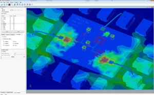 Figure 3. EM visualization
The design workflows for RFICs and mixed-signal ICs are very different from digital IC workflows, as outlined below.
Synthesis
Digital circuits consist of a small number of well-defined logic gates (like NAND). The circuit schematic is converted to a gate-level netlist expressed in a hardware description language like Verilog or very high-speed integrated circuit hardware description language (VHDL). During routing and placement, these gate-level constructs are then converted to on-wafer cells defined by the cell libraries in the selected fab’s process development kit (PDK).
In contrast, RF and mixed-signal ICs are analogue circuits with unique custom designs. The arrangements of resistors, inductors, capacitors, and active components into amplifiers, mixers, or other subsystems are often unique to each IC. They are not readily distillable into standard cells like digital gates are.
Instead, each subsystem is individually converted into on-wafer structures and interconnects. For example, an oscillator may utilise a complex configuration of transistors in feedback loops. The foundry PDKs for RFICs do provide process information, design rules, and models for active and passive components, but they are not as simple or standardised as digital ICs.
Simulation
In digital chip design, the digital nature of signals makes simulations relatively simpler. Digital IC simulations include various digital inputs and timing analyses.
In contrast, RFICs must contend with an infinite set of continuous high-frequency waveforms. Noise, parasitic effects, electromagnetic interference (EMI), and antenna effects emerge from the circuit arrangements as well as the physical on-wafer structures. So, realistic simulations are required at every step throughout the design cycle.
Verification
Design-rule checks (DRC) and implementation using a field-programmable gate array (FPGA) are common in digital IC design.
DRC verification tools are used in RFIC and mixed-signal semiconductor design as well. However, prototyping an RFIC with an FPGA is rare because its RF characteristics will be totally different. FPGAs are still used to verify the digital portions of mixed-signal ICs.
How do you choose the right EDA tool for a wireless electronic design project?
In addition to accurate RF and EM modelling and simulations, an essential feature is the ability to test the designs against wireless standards (like 5G and 802.11ad) right from the start.
This is possible using design tools that include virtual test benches (VTBs) for all the major wireless standards. VTBs ensure that the designs stay within the thresholds that standards place on signal power, noise, interference, and more.
What are the main challenges faced when using EDA tools in complex 3D circuit design?
Some of the main challenges in 3D RF circuit design include:
- modelling electromagnetic behaviours in 3D
- impedance matching
- noise
- linearity
- stability
- power consumption
- electromagnetic interference
- problems caused by increasing densification, like integrating different materials, 3D integration, and advanced packaging
What are the key features to look for in EDA tools for effective RFIC Design?
For effective design of RFICs and mixed-signal ICs, look for these key features:
- Advanced simulation algorithms developed for Keysight RF instrumentation and Keysight RF EDA software ensure equivalent results between virtual simulations and physical measurements.
- Fast-envelope techniques, compact test signals, and distortion EVM make simulation run times practical for RFIC designs in data-intensive, high-bandwidth mmWave or sub-THz applications, including 5G/6G, electric vehicles, and AI-enabled systems.
- Authentic waveforms and VTBs incorporate system context when simulating designs, enabling teams to optimise RFIC designs for their intended system applications sooner and successfully integrate first-pass into physical devices and systems.
Keysight RFIC EDA tools
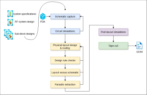 Figure 4. Keysight RFIC EDA tools
Keysight’s ecosystem of EDA tools streamlines RFIC and mixed-signal IC design, simulation, and verification. For large design teams looking for high productivity, the Keysight designcloud enables offloading RF and EM simulations to high-performance cloud platforms for rapid results and quick design cycles. The main design and simulation tools for RFICs and mixed-signal ICs are outlined below.
Keysight Advanced Design System (ADS)
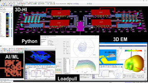 Figure 5. Keysight ADS
The Advanced Design System is tailored for high-frequency RFIC and mixed-signal IC design and simulation. It achieves 3D heterogeneous integration (3DHI) of RFICs, MMICs, packaging, PCBs, and antennas using multi-technology modules. Key features are listed below.
- Multi-technology integration: ADS enables comprehensive 3D integration of chips, packaging, interconnects, and boards, facilitating realistic simulations of assembled products.
- Superior simulation capabilities: The platform’s advanced circuit-level RF simulations and EVM optimisations for mixed-signal ICs produce predictions that are close to real-world measurements.
- Comprehensive component libraries: The platform offers vendor component libraries and PDKs that include symbols and layout footprints, as well as high-accuracy RF and microwave models.
- Standards compliance: ADS enables verification against wireless standards like 5G, automotive radar, and 802.11ad.
- Flexible automation: ADS supports Python scripting for automation and integration with external applications like artificial intelligence (AI) and machine learning (ML) to streamline design and verification workflows.
RFIC Design (RFPro Circuit)
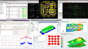 Figure 6. RFPro Circuit
RFPro Circuit is a specialised software for RFIC design. It can:
- model components on silicon chips accurately
- optimise designs with sweeps and load-pull analysis
- simulate RF designs in the Cadence Virtuoso and Synopsys Custom Compiler environments
- increase performance using Monte Carlo and yield analysis
- Assess error vector magnitude (EVM) for the latest communication standards early in the design phase
- Use the latest foundry technology immediately
Keysight RFPro
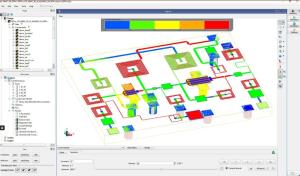 Figure 7. RFPro
RFPro enables RFIC and MMIC designers to run interactive electromagnetic-circuit co-simulation for tuning and optimising their circuits. It includes 3D planar and full 3D finite element method EM simulators.
How are AI and ML algorithms integrated into Keysight RFIC EDA tools?
PathWave ADS provides Python application programming interface (API) endpoints for integrating AI frameworks like TensorFlow and PyTorch. This enables the use of advanced artificial neural network models in the design, modelling and simulation workflows.
How is Python integrated with Keysight EDA tools?
Keysight EDA tools provide Python API endpoints that expand custom features and improve usability.
For example, Python scripts can be used to control data analysis, simulators, and processes.
Python scripts enable the training of custom AI-based simulation models that are trained on measured or published data.
The post EDA Tools for Robust RFICs and Mixed-Signal ICs appeared first on ELE Times.
India’s Vision for 6G: Use-Case Driven Innovation and AI-Enabled Networks
Courtesy: Jessy Cavazos, 6G Solutions Expert, Keysight Technology

As the world prepares for the next leap in wireless technology, India is shaping a bold and inclusive vision for 6G, one that goes beyond speed and latency to address real-world challenges. In a recent interview, Mohmedsaeed Mombasawala, Keysight’s General Manager for Industry Solutions in India, and a key contributor to 6G research efforts in India, shared insights into how the country is approaching 6G with a unique blend of pragmatism, innovation, and social impact.
A Use-Case First Philosophy
India’s 6G strategy is fundamentally use-case driven, a departure from traditional infrastructure-first rollouts. Rather than focusing solely on technical specifications or spectrum availability, the country is prioritising solutions that address societal needs, especially in sectors like agriculture, healthcare, and logistics.
This approach is particularly relevant for India’s vast and diverse population, where connectivity gaps persist in rural and remote areas. Mombasawala emphasised that 6G must be more than a technological upgrade: it must be a platform for transformation.
“We’re not just building networks. We’re building solutions for farmers, doctors, and supply chain operators,” he explained.
By anchoring 6G development in real-world applications, India aims to ensure that the technology delivers tangible benefits to communities that have historically been underserved by previous generations of wireless infrastructure.
AI-Native Networks: Intelligence at the Core
One of the most exciting aspects of India’s 6G vision is the emphasis on AI-native radio access networks (RAN). In this model, artificial intelligence isn’t just a tool; it’s a foundational design element. AI will be embedded throughout the network, enabling dynamic spectrum allocation, predictive maintenance, and real-time optimisation of resources.
This shift reflects India’s strength in software and data science, positioning the country to play a key role in intelligent network design. It also aligns with global trends toward more autonomous and adaptive systems, where networks can learn, evolve, and respond to changing conditions without human intervention.
“AI will be central to how we manage, scale, and secure 6G networks,” Mombasawala noted. “It’s not just about efficiency, it’s about enabling new capabilities.”
Spectrum Strategy: Balancing Reach and Performance
While many countries are exploring high-frequency bands for ultra-fast data rates, India is taking a pragmatic approach to spectrum. The focus is on frequency range 3 (FR3) bands, which offer a balance between performance and coverage. These midband frequencies are well-suited for India’s geographic and demographic diversity, allowing for a broader reach without the need for dense infrastructure.
This strategy reflects a deep understanding of India’s connectivity landscape, where rural access remains a critical challenge. By prioritising spectrum that supports ubiquitous coverage, India is ensuring that 6G can serve both urban innovation hubs and remote villages.
Collaborative R&D and Global Engagement
India’s 6G efforts are deeply collaborative, involving academia, startups, industry leaders, and government agencies. Mombasawala highlighted the importance of cross-sector partnerships in driving innovation and ensuring that 6G solutions are both technically robust and socially relevant.
At the same time, India is actively participating in global standardisation efforts, contributing to international dialogues while tailoring its approach to local needs. This dual strategy—global alignment with local customisation—is key to building a 6G ecosystem that is both interoperable and inclusive.
A Blueprint for Inclusive Innovation
India’s vision for 6G offers a compelling blueprint for countries seeking to balance technology innovation with social impact. By focusing on use cases, AI-native design, and inclusive spectrum planning, India is not just preparing for 6G; it’s redefining what 6G can be.
This approach challenges the notion that next-generation technology must be exclusive or elite. Instead, it positions 6G as a tool for empowerment, capable of transforming lives and industries across the socioeconomic spectrum.
“We want 6G to be a catalyst for change,” Mombasawala concluded. “Not just in how we connect, but in how we live, work, and grow.”
The post India’s Vision for 6G: Use-Case Driven Innovation and AI-Enabled Networks appeared first on ELE Times.
When Silicon Meets the Human Nervous System: A Deep Dive Into Neural Interfaces
Before examining the challenges and opportunities in bioelectronics, it is essential to understand how electronics and the human body converge. The human body—intrinsically organic and biological—can now interact with silicon-based systems through chips, interfaces, and digital extensions that do more than observe; they actively influence physiological function and enable measurable outcomes.
At its core, the human nervous system is among the most sophisticated electrical networks known. Every sensation, movement, and cognitive process originates as an electrical impulse transmitted across billions of neurons. Bioelectronics builds on this foundation by developing electronic systems capable of reading, interpreting, and modulating these neural signals with high precision.
At the centre of this convergence lies neural interface technology—where electronics, materials science, neuroscience, and computation intersect. What began as experimental neural signal recording has evolved into intelligent, closed-loop systems designed to interact with the nervous system in clinically and functionally meaningful ways.
The Nervous System: An Electrical Network
To call the human nervous system an electrical network is to acknowledge the fact that neurons communicate via action potentials—brief voltage changes produced by ionic movement across cell membranes. These electrical impulses propagate along nerve fibres and form the basis of basic human senses, including perception, motion, and cognition.
However, from an engineering standpoint, neural activity resembles a signal source but with certain riders. The biological signals that the neurons communicate through are characterized distinctly from conventional electronic systems in the following ways:
- Extremely low amplitude (microvolt range)
- Highly variable across individuals
- Sensitive to physiological and environmental conditions
- Embedded in a noisy, living medium
These complexities change the entire course of the environment and approach, which is a crucial aspect of the electronics system design, and that’s why bioelectronics is not simply applied electronics—it is fundamentally a new class of system design.
The Neural Interface Challenge
A neural interface is the physical and electrical bridge between living tissue and electronic systems. Basically, it is a technological innovation that enables a direct communication pathway between the brain (nervous system) and an external device, allowing thoughts/neural signals to control machines, and machines to send sensory data back to the brain. Its primary functions are twofold:
- Reading neural signals
- Delivering electrical stimulation
This makes the landscape more challenging, owing to the complex mix of an artificial arrangement to be balanced with a natural or organic system, and making it perform efficiently and adaptively. To this effect, the challenge lies at the interface level itself. Electronics are rigid and static; biological tissue is soft, adaptive, and reactive. Any long-term interface must balance electrical performance with biocompatibility.
Key Challenges in such an arrangement include:
- Mechanical mismatch between electrodes and tissue
- Immune responses that degrade signal quality
- Corrosion in ionic biological environments
- Stability over years, not months
Dr. Ben Rapoport, Co-founder and Chief Science Officer of Precision Neuroscience- the rival of Neuralink, notes that innovation is increasingly focused on minimising invasiveness: “That’s a big misconception, he said. People often incorrectly assume that ‘you need electrodes that penetrate deep inside the brain to get that information out.”
He further adds that Precision lies in developing a thin film that sits on the brain and records the brain activity. This reflects a broader industry trend toward surface-level and flexible neural interfaces rather than deep, rigid implants.
Neural Interfaces Making Gradual Emergence
Industry experts increasingly emphasise that neural interfaces are no longer speculative technologies. Yet these are gradually making space in our lives, making them more common in overall human behavior.
According to Kevin Hughes, Information Scientist of the Chemical Abstracts Service (CAS), which tracks emerging science and engineering domains, “With the recent news that Neuralink is approved to begin human trials, it’s clear that bioelectronics like brain-computer interfaces (BCIs) are moving out of the realm of science fiction and into reality.”
In the very same continuity, he also points out the difference that the industry is witnessing between the number of journals and the number of patents filed in the biotechnology landscape. The following graph shows the starkly lower number of commercial patents, while academic research has outpaced the same in the last 5 years. He writes, “his suggests that large-scale commercialization of these technologies faces fundamental scientific challenges that are being studied at the academic level and may be years away.”
Capturing Neural Signals: An Analog Problem
Neural signal acquisition is fundamentally constrained by analog design challenges. Electrical signals captured at neural electrodes typically exist in the microvolt range, making them highly susceptible to corruption from noise sources such as muscle activity, motion-induced artefacts, electrode impedance variability, and external electromagnetic interference. Unlike many conventional sensing environments, the biological interface itself is dynamic, lossy, and electrically unstable.
To this effect, the front-end electronics gets to play the most decisive role. These must provide:
- Ultra-low-noise amplification
- High input impedance
- Strong common-mode rejection
- Extremely low power operation
Unlike conventional sensors, neural interfaces cannot rely on static calibration. Signal properties drift over time due to biological adaptation and tissue response, demanding adaptive hardware and software co-design. Consequently, effective neural signal acquisition increasingly relies on adaptive architectures, where analog hardware, digital signal processing, and software algorithms are co-designed to track signal drift, compensate for variability, and maintain reliable performance over extended operational lifetimes.
From Signals to Interpretation
Raw neural signals carry no explicit meaning. Interpretation requires computational models capable of identifying patterns associated with intention, perception, or pathology. This has made way for Machine learning, hence making it central to modern bioelectronics. Models must continuously adapt as neural signals evolve, making on-device intelligence essential and timely.
According to BIOS Health, a company focused on AI-driven neural interfaces, this represents a new data modality in medicine:
“At BIOS, we’re developing AI-powered neural interfaces to allow us to read and write neural signals as a new data modality in healthcare… we can decode it, use biomarkers to see how a disease is progressing, and we can change those electrical signals. In doing so, we’ve delivered a therapeutic—we’ve treated a disease.”
This highlights a shift from monitoring systems to active bioelectronic therapies.
Writing to the Nervous System: Electrical Stimulation
Neural interfaces are not limited to passively observing neural activity; they are equally defined by their ability to actively influence the nervous system. This capability is most clearly demonstrated in modern bioelectronic devices that deliver precisely controlled electrical stimulation to targeted neural pathways. By injecting carefully shaped electrical pulses, these systems can alter neural firing patterns in ways that restore, suppress, or modulate biological function.
Electrical stimulation underpins a wide range of therapeutic and functional outcomes, including:
- Restoration of sensory input
- Modulation of dysfunctional neural circuits
- Enablement of motor control
- Suppression of chronic pain signals
From an engineering standpoint, effective neural stimulation demands precise control over parameters such as pulse amplitude, width, frequency, and waveform shape. These parameters must be tailored not only to the targeted neural population but also to long-term safety constraints, including charge balancing and tissue compatibility. Overstimulation risks tissue damage or neural fatigue, making precision and reliability non-negotiable design requirements.
Increasingly, neural stimulation systems are evolving into closed-loop architectures, where real-time sensing, on-device computation, and adaptive stimulation form a continuous feedback cycle. Instead of delivering fixed stimulation patterns, these systems dynamically adjust outputs based on measured neural responses, enabling more personalised, efficient, and clinically effective interventions. This shift from open-loop to closed-loop control represents a critical step toward truly intelligent bioelectronic systems.
Case Study: Cochlear Implants
Cochlear implants remain one of the most successful examples of bioelectronics in practice. Rather than amplifying sound acoustically, cochlear implants convert audio signals into electrical stimulation patterns delivered directly to the auditory nerve. Frequency components are mapped spatially along an electrode array implanted in the cochlea.
Despite delivering a simplified representation of sound, cochlear implants exploit the brain’s neural plasticity. Over time, users learn to interpret these electrical patterns as meaningful auditory experiences. From an engineering perspective, cochlear implants demonstrate:
- Long-term biocompatibility
- Ultra-low-power embedded processing
- Robust signal mapping
- Effective closed-loop adaptation
They validate the principle that bioelectronics succeeds when it works with biology rather than attempting to replicate it perfectly.
Power, Reliability, and Longevity
Implanted bioelectronic systems must operate reliably for years without failure. Power consumption, heat dissipation, and battery safety are critical constraints.
Unlike consumer electronics, failure carries direct clinical risk. As a result, bioelectronic design prioritises stability, redundancy, and conservative validation over rapid iteration.
Conclusion
The future of bioelectronics lies in deeper integration and softer interfaces—flexible electronics, bio-compatible materials, and adaptive systems that learn continuously. As silicon systems become more biologically aware, neural interfaces are evolving from experimental tools into foundational technologies for healthcare and human–machine interaction.
Bioelectronics does not aim to replace the nervous system. It aims to understand it—and, where possible, support it—using electronics designed to operate on biology’s terms.
The post When Silicon Meets the Human Nervous System: A Deep Dive Into Neural Interfaces appeared first on ELE Times.
Government’s Green Signal to 22 projects under ECMS
The Ministry of Electronics and IT has supposedly approved 22 new projects under the Electronics Components’ Manufacturing Scheme on January 02, 2026, with a projected investment of ₹41,863 crore and production of ₹2,58,152 crore.
The said proposals include those from Dixon, Samsung Display Noida Pvt Ltd, Foxconn (Yuzhan Technology India Pvt Ltd), and Hindalco Industries. These are expected to provide nearly 33,791 direct employment opportunities. This approval comes after the Ministry approved 24 proposals under the ECMS earlier.
The approval letters were handed directly by Union Minister Ashwini Vaishnav to those part of the above 22 projects on Friday.
As per a background note circulated by the Ministry on the third tranche of approvals, the nod includes the manufacturing of 11 target segment products that have cross-sectoral applications, such as mobile manufacturing, telecom, consumer electronics, strategic electronics, automotive, and IT hardware.
Of 11 products, 5 are bare components such as PCBs, Capacitors, Connectors, Enclosures, and Li-ion Cells; 3 pertain to sub-assemblies such as Camera Modules, Display Modules, and Optical Transceivers; and 3 are supply chain items such as Aluminium Extrusion, Anode Material, and Laminate.
The background note said the approvals aim to significantly strengthen domestic supply chains, reduce import dependence for critical electronic components, and support the growth of high-value manufacturing capabilities in India.
The post Government’s Green Signal to 22 projects under ECMS appeared first on ELE Times.
Beyond technology: ST’s commitment to educating and inspiring next generation
ST is well known as a global company creating technology and driving innovation. But it’s not just that. Its role extends beyond manufacturing products: the company is committed to inspiring and educating future generations by supporting scientific research, STEM initiatives, and engaging in talent development. This article provides an overview of ST’s recent and ongoing educational activities across key regions, including Italy, France, Singapore, and the United States.
Activities Across STEM, university relations and talent developmentST maintains a strong presence in the communities where it operates, participating in local and national events. Through various initiatives, the company connects with a broad spectrum of audiences, from primary and secondary school students and university graduates to experienced researchers. This commitment is further amplified through the ST Foundation, which leverages technology and education to drive social progress, promoting digital inclusion for disadvantaged communities globally. Regardless of the audience’s level of expertise, ST’s goal remains the same: promoting scientific culture and making the complex processes that lead to the production of our chips understandable.
Recent educational events in ItalyIn Italy, ST organises more than 200 events annually, reaching approximately 18,000 students ranging from preschool to high school and university. Below are some of the key initiatives we’ve recently organised.
Neapolis Innovation Summer Campus Participants at Neapolis Innovation Summer Campus
Between late August and early September, the ST site in Arzano (Naples) hosted the twelfth edition of the Neapolis Innovation Summer Campus in collaboration with five universities in Campania. This annual ten-day training program is intended for bachelor’s and master’s degree students who want to explore the use of 32-bit microcontroller platforms and seek an opportunity to interact with industry experts. The initiative offered intensive, hands-on seminars at the ST site and provided a kit of components for the project work that students presented at the end of the event. Additionally, the event hosted small and medium enterprises and start-ups throughout its entire duration, allowing them to present themselves and build connections with young talent.
Researchers’ Night in MilanIn September 2025, ST took part in the Researchers’ Night in Milan, an event promoted by the European Commission as part of the Marie Skłodowska-Curie Actions, hosting research centres, institutions, universities, and organisations engaged in scientific dissemination. ST showcased its Edge AI technology: one of the demos included the LSM6DSV80X sensor with the STEVAL-MKI247A board, connected to the SensorTile.box PRO, and demonstrated how to monitor high-impact activities in soccer (for example, between the player’s shoe and the ball) and collect valuable information for game analysis.
Maker Faire Rome – European Edition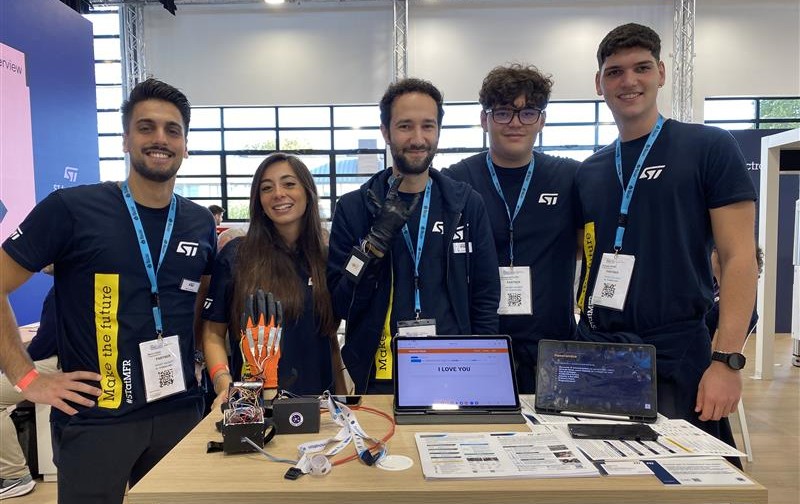 The STEM student winners of the 12th edition of the Neapolis Innovation Summer Campus 2025 with the smart glove “Hermes’ Hand”.
We also participated in Maker Faire Rome – European edition. This annual event has a varied audience, from school to university students, to startups, companies, and government institutions. Visitors could interact with demos in different fields, such as electronics, augmented reality, artificial intelligence, robotics, gaming, music and art. ST organised workshops covering Edge AI, robotics, and the STM32 Open Development Environment. A highlight was the “Hermes’ Hand”, a smart glove developed by a STEM student of the 12th edition of the Neapolis Innovation Summer Campus 2025. This project uses the STM32G474RE, X-NUCLEO-IKS4A1, and custom-made MEMS sensors to translate one’s voice into sign language in real time, breaking down communication barriers.
Science Festival in Genoa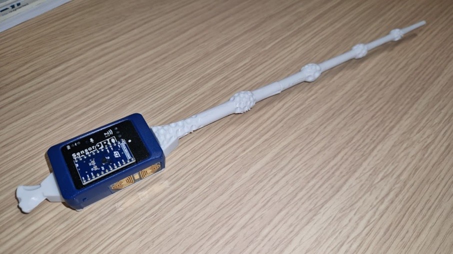 The “magic” wand demo
Another event held at the end of 2025 and aimed primarily at young students and families was the Science Festival in Genoa. ST presented “AI in your hands”: a magic wand, waved by visitors, demonstrated how the Integrated Signal Processing Unit (ISPU) in MEMS sensors can process movement locally (at the edge). Limited dependence on the cloud ensures high response speed, low power consumption, and greater security. Behind the playfulness and the visitors’ amazement, therefore, there was not magic but rather powerful local data processing.
Agreement with Polytechnic University of Turin
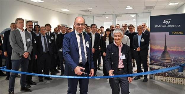 Inauguration of ST’s new design centre at the Polytechnic University of Turin. In the picture, Pro-Rector Elena Baralis and CEO of STMicroelectronics Italy Alberto Della Chiesa
To strengthen its ties with universities, in October, ST and the Polytechnic University of Turin renewed their framework agreement for the next four years and celebrated the inauguration of a new ST design centre space. The collaboration focuses on research and training of undergraduate and graduate students, particularly in fast-evolving fields such as cybersecurity, AI, and energy efficiency. Since 2019, STMicroelectronics has hired over 200 graduates (bachelor’s, master’s, and doctoral degrees) from the Polytechnic University of Turin. Many undergraduate and graduate students also work on their theses with the help of ST employees at the Turin centre.
Educational initiatives in FranceIn France, there is a virtuous example showing how recruitment needs in the field of microelectronics can favour high-level training for students and professionals. ST is one of the actors in the I-NOVMICRO program, a consortium of different companies that promotes microelectronics and electronics careers and provides advanced training in the Southern French Region (Rousset, Toulon, Sophia-Antipolis).
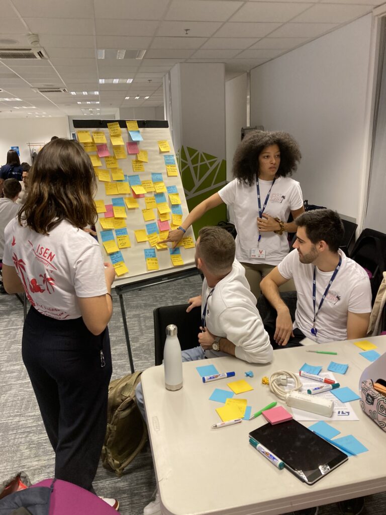 Participants at I-NOVGAME
Launched in 2019, this initiative directly addresses recruitment needs by offering specialised training that qualifies people for technical sectors, particularly manufacturing jobs. Since the beginning of the project, more than 15,000 people have been trained, from secondary schools to baccalaureate level. This program allows students to learn semiconductor manufacturing processes in real-world conditions: facilities include an educational clean room and an educational grey room dedicated to maintenance training. The program also finances and leads a network of 12 Fab Labs in local high schools, coordinated by ST Rousset, and promotes STEM disciplines through school visits. The project’s ambition is to reach out all the whole of France and then expand on a European scale.
I-NOVMICRO also includes:
- I-NOVGAMES, an STM32 engineering and application challenge involving six engineering schools.
- INNOV ISLAND, a dynamic Metaverse offering a digital and 3D environment for training, educational materials, conferences, and job dating for students and employees.
Beyond direct training, ST supports education through donations of unused laboratory equipment, computers and STM32 microcontroller boards every year to schools and partners. Our company also offers career guidance through diverse programs and initiatives, primarily focused on engaging young people and supporting students with disabilities:
- For industrie, l’Univers Extraordinaire is a digital educational event which presents industry professions to young people through video game formats. ST participation includes virtual tours of ST facilities, video interviews with Rousset employees, and live presentations by industry professionals.
- Programs for students with disabilities at the Rousset site. Voyage au cœur de l’entreprise (VACLE) allows eight pupils to explore a dozen different professions over the course of a week, while Mentorat au coeur de l’entreprise (MACLE) is a mentorship program for high school students, where volunteer employees support students throughout their academic career, helping them plan their future, understand corporate culture, and develop their soft skills.
 On the left, participants at For industrie. On the right, a videogame screenshot.
Open-source and hands-on education with universities and partners in the US
On the left, participants at For industrie. On the right, a videogame screenshot.
Open-source and hands-on education with universities and partners in the US
ST products and solutions can be useful for developing open-source programs. In the United States, for example, ST contributes to research and education by developing open-source curricula with a strong emphasis on hands-on learning. Professors at the universities we collaborate with (including MIT, UCLA, UC Berkeley, Rensselaer Polytechnic Institute, UC Santa Cruz, and Santa Clara University) use ST development tools, such as the popular STM32 microcontroller platform, in their courses, which are then publicly available on our website. One main area of development now is to adapt the existing curricula to the AI era, which is strongly affecting the job market and how students interact with hardware and firmware programming. For this reason, ST is working with organisations like the MIT CSAIL Alliances (Computer Science and Artificial Intelligence Laboratory) on research, particularly regarding AI computing on devices at the edge and applications in robotics.
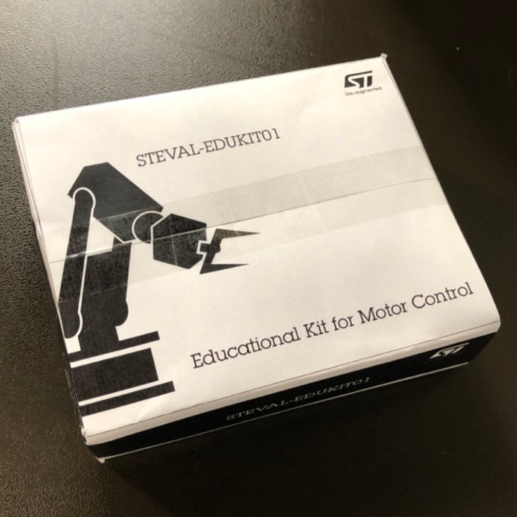 The STEVAL-EDUKIT01
Furthermore, we collaborate with partners who share our vision. With ARM, we have formed an Educational Alliance to support new curricula that will help students gain the necessary skills to become the professionals of the future. Some of these programs were developed in collaboration with the university and published on EdX, reaching over 40,000 enrollments over a four-year period. ST, SparkFun (member of ST Partner Program), DEKA and the Worcester Institute of Technology developed the Experiential Robotics Platform (XRP), an open-source platform for STEM education. Among other things, the XRP is the main provider of educational kits for the FIRST Robotics Competition, the largest STEM competition in the world, which targets primary and secondary schools and registered 785,000 participants in the 2024-25 school year.
Educational initiatives have helped ST products become among the most popular educational products in the United States. The STEVAL-EDUKIT01, developed in collaboration with UCLA, is the first ST development kit designed specifically for education and offers teaching materials for motor control and control systems.
Skills development and positive social impact in Singapore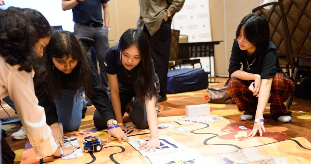 Participants at the STEM Fest organised by United Women Singapore
In Singapore, ST is adopting an educational approach that spans the entire learning journey, from primary schools to higher education. The goal is to drive a positive social impact and bridge the skills gap in semiconductor manufacturing by aligning education with industry needs. This comprehensive approach also focuses on inclusion addressing gender imbalance in the industry. To this end, ST partners with the United Women Singapore (UWS) to implement STEM initiatives for girls, such as the UWS STEM Fest. These initiatives provide mentorship, coaching, and networking to encourage more women to pursue STEM careers. Furthermore, ST fosters creativity and social responsibility in partnership with the Singapore Institute of Technology through the SIT Community Challenge. This program challenges students to develop sustainable technology solutions addressing real-world community issues such as urban mobility and environmental sustainability, directly supporting Singapore’s Smart Nation goals.
ST collaborates with Universities like the Singapore Institute of Technology (SIT) and the Institute of Technical Education (ITE). Our company develops and reviews curricula in microelectronics and semiconductor manufacturing through faculty exchange programs, ST guest lectures and participation in academic advisory committees to ensure relevance to industry demands. Additionally, ST provides practical experience through extensive vocational training, including the Integrated Work-Study Program (IWSP) in collaboration with SIT and Work-Study Diplomas (WSDip) offered by ITE, which provide students with up to 12 months and two years, respectively, of internship experience alongside ST professionals.
ST also invests in future talents through scholarships, including the Singapore Industry Scholarships (SgIS) and the Engineering and Tech Programme Scholarship (ETPS), which support students from pre-university through tertiary education. The flagship STICan (ST I Can) Work Experience Program (WEP) offers students aged 15 to 22 internships across the semiconductor value chain, from R&D and chip design to wafer fabrication and marketing. The program provides technical exposure and personal development courses to prepare students for university and careers.
ConclusionST’s engagement in educational and STEM activities serves a dual purpose: cultivating the next generation of talent while contributing to societal progress. From university partnerships to global outreach events, these initiatives form the foundation of ST’s commitment to driving innovation and developing technology responsibly for the future.
The post Beyond technology: ST’s commitment to educating and inspiring next generation appeared first on ELE Times.
How 2025’s Constraints Became the Blueprint for Electronics System Design in 2026?
As the electronics industry looks back at 2025, a clear shift toward efficiency, miniaturisation, and—most critically—more deliberate material choices becomes evident. The year stands out as a pivotal phase in the evolution of electronics, enabling systems tailored to the increasingly demanding requirements of data centres, advanced sensing platforms, electrified systems, and next-generation semiconductor packaging. Rather than chasing raw performance, the industry in 2025 was forced to reconcile ambition with practicality—balancing sustainability goals, high-performance demands, and mounting geopolitical pressures.
Escalating power densities driven by AI-centric data centers and electrification, shrinking thermal headroom resulting from aggressive miniaturization and higher levels of integration, and growing material availability constraints shaped by geopolitics and post–Moore’s Law design dependencies collectively emerged as defining parameters in the system architectures of automotive, industrial, and infrastructure electronics.
“Performance scaling today is increasingly driven by materials-centric advanced packaging,” says Suraj Rengarajan, Head of Semiconductor Product Group, Applied Materials India. As the industry enters a new year, these forces offer a clear lens through which to examine the design choices and innovations that defined electronics in 2025. Further, to give a better idea of how electrical design is changing in its basics, Suraj from Applied Materials India adds that System-level power, performance, area, and cost are now set by co-optimizing the bonding interface, low‑k dielectrics, redistribution-layer etch, barrier/seed, copper fill, and CMP, and thermal interfaces, treating interconnect resistance and heat flux as primary design variables.
In every aspect that we will be examining in the course of our story, we will try and see how the new dynamics of the industry shaped the preferences of the design engineers to sustain the innovations and applications, including data centres, automotives, and industrial applications.
Power Efficiency over Capability!
As the electrification phenomenon rapidly spread its wings, power efficiency, and not power capacity, became the primary constraint. As the demand across the sectors increased, it raised the energy demands significantly while simultaneously tightening thermal and sustainability limits. This realisation brought the power electronics landscape into the core architectural consideration of an electrical design engineer. In such a condition, the industry moved to significantly increase the power handled per unit area- Power Density.
With AI workloads driving processor currents from a few hundred amperes to well over a thousand—without any meaningful increase in board or package footprint—power efficiency emerged as the only viable path to sustain compute scaling.
This enabled the engineers to focus on more basic and intrinsic aspects of power electronics, which as efficiency, facilitating the same at every level of electronics design. To sustain the new dynamic, the industry moved towards Wide Band-gap (WBG) technologies, including Silicon Carbide (SiC) & Gallium Nitride (GaN). This helped the engineers to prevent switching and conduction losses along with heat generation per unit area, while abiding by tighter thermal and packaging constraints. The WBG technology also pushed the efficiency of the electronic product significantly at the system level.
As power density increased, thermal removal became progressively harder, creating a self-reinforcing loop in which higher efficiency was required simply to preserve thermal headroom rather than to improve performance.
Application
In data centres, rising compute density is driving demand for compact, high-efficiency power solutions. Gallium nitride–based power supplies are gaining traction by improving efficiency, enabling higher switching frequencies, shrinking passive components, and reducing cooling needs. In some architectures, GaN also allows simplified or single-stage power conversion, lowering losses and bill-of-materials complexity while supporting higher voltages closer to the point of load.
“With AI workloads, processor current levels have scaled from a few hundred amperes to over a thousand amperes, while the physical footprint has remained largely unchanged. This has fundamentally pushed power density and efficiency to the centre of system design,” says Dr Kaushik Basu, Associate Professor at IISC Bangalore.
Thermal Limits Over Advanced Cooling
As power efficiency improvements enabled higher power densities, overall heat generation continued to rise—driven by increasing absolute power levels and the closer packing of heat sources within shrinking form factors. Under these conditions, heat was generated faster than it could be spread or dissipated, leading to steeper thermal gradients that placed greater stress on materials, interconnects, and interfaces. At the same time, as electronics moved toward more miniaturised, efficient, and reliability-critical designs, the cost, complexity, and reliability penalties associated with ever-more advanced cooling solutions became increasingly prohibitive.
“As power density increases, heat removal becomes increasingly difficult. That is why efficiency is no longer optional—there is simply no thermal headroom to absorb losses,” says Dr Basu. By 2025, the industry reached a clear realisation: cooling complexity could no longer scale indefinitely to offset rising power density. This marked a fundamental shift in design philosophy, with heat dissipation moving from a downstream mechanical consideration to a primary architectural constraint addressed early in the design cycle. “Designers are increasingly treating materials as first-class design parameters. For advanced nodes, device physics is fundamentally materials physics, ” says Suraj from Applied Materials India.
The growing adoption of advanced packaging approaches, including 2.5D and 3D packaging, was driven as much by electrical constraints as thermal ones, as rising currents made long power-delivery paths increasingly untenable due to conduction losses and localized heating. It emerged as the first line of defence against thermal stress, playing a critical role in protecting silicon devices while enabling higher levels of integration and system efficiency. Particularly, in vertically stacked 3D architectures, where multiple dies are interconnected using through-silicon vias (TSVs), thermal challenges become particularly acute due to limited heat escape paths and the formation of localised hotspots.
In such configurations, traditional air- or liquid-based cooling, or the addition of increasingly sophisticated cooling hardware, often proved insufficient, expensive, or impractical—especially in automotive, industrial, and infrastructure applications with stringent reliability and lifetime requirements. While advanced packaging shortened interconnect paths and reduced resistive losses, it also concentrated heat generation within smaller volumes, making thermal constraints more visible rather than eliminating them. “Teams now co‑simulate variability and reliability, electromigration, bias temperature instability, and time‑dependent dielectric breakdown, at the materials level alongside logic and layout,” says Suraj. As a result, thermal-aware system architecture and packaging design became indispensable in sustaining performance and reliability.
“Advanced packaging approaches such as 2.5D and 3D integration are largely driven by the need to minimise current paths and conduction losses by bringing power conversion closer to the load. However, they also make thermal challenges more visible rather than eliminating them,” says Dr Basu. Eventually, to enable the engineers to accurately predict and manage heat generation and dissipation, which is crucial for preventing component failure, optimizing performance, and ensuring safety, Thermal modeling and co-simulation have now become integral to modern electronics design.
Materials as a Design Constraint, Not a Specification
In 2025, materials in electronics moved beyond being passive specifications and emerged as hard design constraints shaping system architecture from the outset. Persistent supply-chain fragility, geopolitical uncertainty, tightening environmental regulations, and the escalating demands of AI, high-performance computing, and electrification collectively forced designers to treat material selection as a primary limiting factor influencing performance, reliability, and manufacturability.
Midway through the year, the surge in AI, HPC, and electrified platforms imposed unprecedented thermal and electrical stress on electronic systems. Materials able to withstand high power density, heat, and long lifetimes became critical design constraints, shaping device selection, power architecture, and packaging. As advanced nodes and 2.5D/3D integration pushed miniaturisation to its limits, thermal conductivity, mechanical strength, and interconnect reliability emerged as central concerns.
By late 2025, regulatory pressures further reshaped material decisions. Stricter sustainability and environmental compliance requirements, including tighter enforcement of RoHS and REACH norms, transformed lead-free, recyclable, and low-emission materials from preferences into mandatory design conditions. While breakthroughs in advanced materials and AI-driven material informatics offered new optimisation pathways, they also demanded deeper material awareness from system designers.
“We are reaching a point where clever system-level design alone is not sufficient. Addressing today’s power and thermal challenges increasingly requires improvements at the material and device level,” says Dr Basu.
Together, these forces marked 2025 as the year when material availability, compliance, and physics converged, redefining what was practically achievable in electronics design. Material choice ceased to be a downstream optimisation exercise and instead became a foundational variable that set the limits for efficiency, scalability, and long-term system viability.
Conclusion: Designing Within Limits Became the New Competitive Advantage
Power density, thermal limits, and materials are no longer independent design considerations; in high-performance systems, each now defines the operating boundary of the others. “Thermal management and power density will remain the most difficult challenges in the coming years, while material-level improvements, although critical, will take longer to mature,” says Dr Basu.
The defining lesson of 2025 was rooted in a collective shift in how electronic systems were conceived and engineered. As power efficiency replaced raw capability, thermal limits supplanted aggressive cooling, and materials evolved from passive enablers to active constraints, electronics design entered an era governed less by ambition and more by physical and systemic realities. “Efficiency is being engineered from the materials up, with interconnects, dielectrics, power delivery, cooling, and packaging treated as a coupled system,” says Suraj of Applied Materials India.
Across data centres, automotive platforms, and industrial systems, engineers confronted hard limits of heat, materials, and long-term reliability, making performance something to be balanced rather than maximised. Power electronics moved to the centre of system architecture, packaging became a critical thermal and electrical optimisation layer, and material choices began shaping designs at the architectural stage. Innovation did not slow under these constraints; it became more disciplined, integrated, and system-aware.
As electronics move forward, the lesson of 2025 is clear: the future belongs not to systems that promise peak performance on paper, but to those engineered with a deep understanding of efficiency, thermal reality, and material limits—marking the year when designing within constraints became a true engineering advantage. In an industry long defined by relentless scaling, 2025 will be remembered as the year when designing within limits became the ultimate engineering advantage.
The post How 2025’s Constraints Became the Blueprint for Electronics System Design in 2026? appeared first on ELE Times.
India’s Electronic Exports grow sixfold from ₹1.9 lakh crore to ₹11.3 lakh crore in a decade: Ashiwini Vaishnaw
Sh Ashwini Vaishnaw, Union Minister for Railways, Electronics, and Information Technology, took to his Twitter handle to underline India’s stride in the electronic exports. He points toward India’s ongoing transformation into a global electronics export hub driven by the sharp growth in production, jobs, and investments flowing into the sector, bolstered by various initiatives under the central government, including Make in India, PLI, ECMS, etc.
He writes, “ India’s growth story in electronics manufacturing is PM @narendramodi Ji’s vision of developing a comprehensive ecosystem.” He underlines the government’s continuity and effective oversight over the industry, which is leading to sustained development as well as growing impact on the nation and the world. The image he posted shows how the Make in India initiative has brought about a multiplication in the number of Mobile manufacturing units, from 2 in 2014-15 to 300 in 2024-25.

Electronics: Among the top 3 export categories
For India, out of the total electronics production worth Rs 11.3 Lakh crore in 2024-25, a strikingly high value of Rs 3.3 Lakh crores is attributed to exports, making electronics rank among the top 3 items exported by India. This also marks an eightfold increase in the export of the electronics item in the year 2024-25, rising from 0.38 Lakh crore in 2014-25.

Building Capacity for Modules, Equipment
He writes, “ Initial focus on finished products. Now we are building capacity for modules, components, sub-modules, raw materials, and the machines that make them.” He even goes on to add about the Electronics Component Manufacturing Scheme, wherein he talks about attracting 249 applications received amounting to ₹1.15 lakh crore investment, ₹10.34 lakh crore production, and creating 1.42 lakh jobs. He writes, “It is the highest-ever investment commitment in India’s electronics sector. This shows industry confidence.”
He also touched upon the Production-Linked Incentive (Large Scale Manufacturing-LSM), which enabled the industry to attract over ₹13,475 crore worth of investment. It is equivalent to a Production value of ~₹9.8 lakh crore. He even adds, “ Electronics manufacturing created 25 lakh jobs in the last decade. This is the real economic growth at the grassroots level. As we scale semiconductors and component manufacturing, job creation will accelerate.”
“From finished products to components, production is growing. Exports are rising. Global players are confident. Indian companies are competitive. Jobs are being created,” writes the minister as he shares India’s Make In India Impact Story.
The post India’s Electronic Exports grow sixfold from ₹1.9 lakh crore to ₹11.3 lakh crore in a decade: Ashiwini Vaishnaw appeared first on ELE Times.
ST’s AEK-AUD-C1D9031 making audio more accessible with an SPC58 MCU and a FDA903D in the 1st all-in-one AVAS board
The AEK-AUD-C1D9031 is ST’s latest AutoDevKit automotive development platform for audio applications, enabling engineers to play audio with only a microcontroller rather than a far more costly DSP. It features an SPC582B60E1 general-purpose MCU and the FDA903D Class D audio amplifier, which provides current-sensing capabilities. Hence, not only does this combination allow designers to easily and efficiently add audio applications such as simulated engine sounds, but it can also detect if a speaker is disconnected. Moreover, as a standalone MCU system, it offers enhanced resiliency by operating independently from the main infotainment system.
The booming challenges of bringing audio to cars More than just musicThere’s a lot more audio in cars than most assume. When consumers think about it, they typically envision their entertainment system, which remains a critical component. However, there are chimes, warning bells, notification dings, and so many other audio cues that enhance the user experience. In addition, many of them must be available before the entertainment or even the engine is switched on, meaning that not all of them can rely solely on the sound system that drivers and passengers use to listen to music. Furthermore, since electric cars are so quiet, thanks to the absence of a combustion engine, manufacturers add sounds for safety and to improve the user experience.
More than just a central entertainment systemThe problem is that while audio in cars, and acoustic vehicle alerting systems (AVAS) are far from new, they are also not easy to implement and can easily add to the bill of materials. Indeed, the cost of a DSP, an equaliser, and all the components needed by the audio pipeline can quickly add up, which is why many manufacturers opt for a central entertainment system. The problem is that it is a complex system for what are, in effect, computationally trivial tasks, and engineers need to account for safety considerations. For instance, a critical audio warning must still play regardless of the main speaker volume, which requires the design of safeguards and other complex systems.
More than just carsTeams working on modules are also looking to reuse their systems in many more types of vehicles than just the car they originally had in mind. Whether we are talking about two- or three-wheeler trucks or something as small as a forklift, all require AVAS, and being able to reuse a system across many more platforms provides tremendous economies of scale. However, this isn’t possible when using an entertainment system designed primarily to play music from a phone or the radio. Consequently, more and more makers are taking a different approach to audio alerting systems, exploring solutions that are simpler, more cost-effective, and more flexible.
The resounding solutions of the AEK-AUD-C1D9031 The AEK-AUD-C1D9031
A different melody: a new approach to AVAS
The AEK-AUD-C1D9031
A different melody: a new approach to AVAS
The AEK-AUD-C1D9031 is a development platform that helps car makers approach AVAS differently, and many customers have already adopted it to address these challenges. At its core, it is one of the most straightforward systems possible. Playing sound is as simple as sending power to the module. Thanks to its SPC58 microcontroller, it doesn’t need a complex operating system or workarounds to fit a platform designed to perform a myriad of other functions. The AEK-AUD-C1D9031 even demonstrates how developers can use a dedicated mute pin, which makes turning the sound on and off far simpler. Similarly, the current-sensing feature of the FDA903D amplifier means engineers don’t need to add additional components, thus further reducing the bill of materials.
Familiar tunes: common standards and practicesDevelopers can use standard interfaces, which save significant development time. For instance, they can talk to the flash or program the amplifier via an I2C interface, or use I2S to send audio samples. In practice, programmers can play audio samples directly from storage, further eliminating the need for intermediate steps. Developers will have to sample the sounds, as they cannot use a compression format like MP3. For instance, they can play a pre-recorded engine noise from a traditional uncompressed WAVE file and then attach a potentiometer to an AEK-CON-C1D9031 connector board plugged into the AEK-AUD-C1D9031 to interact with the sound.
Indeed, it is possible to run a demo that modifies the sound output based on potentiometers that users can move sideways. By using bit-shifting, developers can lower or increase the pitch. Similarly, increasing or decreasing the number of samples directly impacts playback speed. Hence, it’s through those mechanisms that developers can simulate an engine accelerating or decelerating without using expensive DSPs or EQs. Similarly, the system can generate one note at a time to reproduce complex melodies without having to play a traditional file. In fact, ST developed a demo that uses AutoDevKit and the AEK-AUD-C1D9031 to play the famous Rondo All Turca.
Music to engineers’ ears: more features, less complexity The AEK-CON-C1D9031
The AEK-AUD-C1D9031 also shows the advantages of a system independent of the central infotainment system. Since the SPC582B60E1 supports CAN bus, plugging our platform into an existing car safety architecture is simple, enabling engineers to trigger critical alerts very quickly. In most traditional systems, offering all these features would require a far more complex integration process. It’s why we have seen module makers adopt the AEK-AUD-C1D9031. By offering the SPC582B60E1 and the FDA903D on a cost-effective platform, we were able to offer a set of features that help them stand apart, without taking away from the budget they had allocated to other, more costly parts of the vehicle, like the battery management system or onboard charging.
The post ST’s AEK-AUD-C1D9031 making audio more accessible with an SPC58 MCU and a FDA903D in the 1st all-in-one AVAS board appeared first on ELE Times.
Indo-German Tech Cooperation Strengthens with German Ambassador’s visit to R&S India
Rohde & Schwarz India extended a warm welcome to His Excellency Dr. Philipp Ackermann, Ambassador of the Federal Republic of Germany to India, during his visit to the corporate facility located in New Delhi. This significant event signifies a notable advancement in the mutually beneficial relationship between Germany and India. The visit is anticipated to foster increased collaboration in the spheres of advanced technology and innovation, further enhancing the partnership between the two nations.
The Ambassador’s visit aimed to throw light on Rohde & Schwarz’s growing presence over the last three decades, along with highlighting the company’s expanding research and development (R&D) capabilities, planned investments in infrastructure, and enhanced technological competencies, which are also in line with the ‘Make in India’ initiative.
Dr Ackermann was given an overview of the company’s state-of-the-art R&D test laboratories, its work in niche electronics technology areas, and its plans for future innovation and growth during his visit, where he also interacted with the engineering and leadership teams to understand their technical capabilities and long-term vision.
His Excellency Dr Philipp Ackermann remarked:
“It is encouraging to see German technology companies like Rohde & Schwarz making long-term commitments in India. The company’s focus on R&D, local competence development, and high-quality engineering reflects the strong foundation of Indo-German cooperation in technology and innovation.”
Speaking on the occasion, Yatish Mohan, Managing Director, Rohde & Schwarz India, stated: “We are deeply honoured to host His Excellency Dr Ackermann at our facility. This visit underscores our commitment to advancing technological excellence in India and reflects the shared vision of fostering stronger economic and innovation ties between our two nations.”
Rohde & Schwarz India is committed to deepening Indo-German industrial collaboration, driving innovation through local R&D initiatives, and contributing to the nation’s self-reliant manufacturing ecosystem.
The post Indo-German Tech Cooperation Strengthens with German Ambassador’s visit to R&S India appeared first on ELE Times.
Сторінки

