
ELE Times

Securing Humanoid Robotics with TPM-Anchored FPGAs
Courtesy: Lattice Semiconductor
The humanoid robotics market is rapidly transitioning from experimental prototypes to early commercial deployments. What once belonged in research labs is now appearing in factories and controlled service environments, driven by advances in sensing, actuation, and edge intelligence.
Humanoids represent what many describe as the ultimate expression of physical AI — but the market is still early. “The market is still early, but it is moving quickly,” says Eric Sivertson, VP of the Security Business at Lattice. “We are seeing humanoid robotics transition from research and pilot stages into early commercial deployments. Humanoids represent the ‘physical AI’ ultimate instantiation, but adoption is not yet widespread — although the momentum is real.”
With companies such as Tesla, Boston Dynamics, Figure AI, and Agility Robotics pushing forward, analysts anticipate a significant inflexion point around 2026–2027.
But scaling humanoids to production-grade systems demands more than innovation. It requires trust.
Reliability Before Scale
Industrial buyers expect 99.99% uptime, seamless integration into human environments, and safe 24/7 operation. Yet developers continue to face challenges in reliability, dexterity, battery life, and real-world autonomy.
Sivertson notes that many prototypes still fall short of industrial expectations: “Utility is one of the most common concerns. Because the technology is still early, many prototypes and pilots fall short of industrial-grade expectations such as 99.99 per cent uptime, continuous 24/7 operation, and safe integration into human environments.”
Among the most persistent technical gaps are dexterity, failure-free operation, and energy efficiency. These challenges push developers toward hardware architectures capable of deterministic, low-latency control.
Determinism at the Hardware Layer
Humanoid systems require dense sensor fusion and sub-microsecond motor control loops. Variable latency is not acceptable when stabilising balance or controlling fine manipulation. Unlike CPUs and GPUs that execute instructions through pipelines, FPGAs implement functionality directly in hardware.
“Unlike instruction-based processors constrained by pipelines, FPGAs implement functionality directly in hardware. That enables critical operations to execute predictably within a single clock cycle,” explains Sivertson. This deterministic execution becomes foundational when motors, joints, and actuators must respond instantly and predictably under all conditions — including fault scenarios.
Security Is Now a First-Order Requirement
As humanoids move into human-shared spaces, cybersecurity becomes inseparable from physical safety.
Sivertson is unequivocal: “With humanoids, it’s impossible to separate safety and security.” A compromised humanoid is not simply a system failure — it can cause physical harm, exfiltrate enterprise data, violate privacy, or coordinate attacks across shared vulnerabilities.
He warns against applying legacy models: “It’s very easy to fall into a square peg in a round hole design fallacy. Humanoids are not traditional IT, industrial robotics, or consumer IoT — even though they incorporate elements of all three.”
Perhaps the most dangerous mindset is postponing security. “Security cannot be bolted on at the end. It must be considered throughout the design process and across the full lifecycle. The idea of ‘functionality first, harden later’ usually introduces more risk than intended.”
TPM-Anchored FPGAs and Hardware Root of Trust
To establish trust at scale, developers are increasingly adopting TPM-anchored FPGA architectures aligned with Trusted Computing Group specifications.
These architectures provide:
- Authenticated boot
- Per-node cryptographic identity
- Secure firmware updates
- Runtime attestation
- Hardware Root of Trust (HRoT)
Sivertson emphasises that TPM alone is not enough in dynamic humanoid systems: “In static systems, TPM-based attestation can sometimes be sufficient. In humanoids, it is only the beginning of an attestation-to-cyber-resilience chain. Active, real-time monitoring and immediate mitigation are also required.”
By combining TPM-based identity with FPGA-enforced deterministic control, developers can embed strong protections at the robot’s most critical physical interfaces. Lock-step redundancy, parallel fail-safe mechanisms, and real-time validation of attack surfaces further reduce cascading risks.
The Safety–Security Tension
One of the more subtle engineering challenges lies in the philosophical difference between safety and security systems.
“In a safety system, you monitor malfunctions and maintain a controlled course of action. In a secure system, if a breach occurs, the response is often to shut down or deny. While the monitoring mechanisms may be similar, the prescribed responses can be fundamentally opposed.” Designing humanoids requires setting clear precedence between these responses — without compromising either domain.
Building Trustworthy Physical AI
As humanoids evolve from pilots to scaled deployments, the competitive advantage will belong to platforms built on trusted foundations. Lattice Semiconductor positions its low-power, Root-of-Trust-enabled FPGAs at this intersection of determinism and embedded security — enabling developers to advance without sacrificing reliability or safety.
The potential of humanoids is enormous. But as Sivertson suggests, the responsibility is equally significant. The future of physical AI will not be defined solely by dexterity or autonomy — but by whether these machines can be trusted to operate safely in the real world.
The post Securing Humanoid Robotics with TPM-Anchored FPGAs appeared first on ELE Times.
Keysight Expands Digital‑Layer Error Performance Validation for High‑Speed 1.6T Interconnects in AI Data Centres
Keysight Technologies, Inc. introduced the Functional Interconnect Test Solutions (FITS) portfolio and FITS-8CH, the suite’s first product. FITS-8CH delivers digital-layer bit error ratio (BER) and forward error correction (FEC) performance validation for high-speed optical and copper interconnects used in network equipment and production network infrastructures.
As interconnect speeds increase and designs grow more complex, manufacturers of chips, optical and copper interconnects, and network equipment face mounting pressure to ensure reliability before products reach mass production and throughout the manufacturing process. Traditional physical-layer test tools play a vital role in validating electrical lanes against industry specifications, establishing a strong compliance baseline. Building on this foundation, system-level validation helps extend insight into the performance of fully integrated interconnects and operational sub-assemblies, including error behaviour in realistic environments.
Accurate assessment of real‑world system conditions is only possible when all interconnect electrical or optical lanes undergo high-speed error-performance validation. Without this testing, the risk of production delays or costly failures in the field increases. This includes validating error performance for high‑speed PAM4 electrical lanes operating at 53 Gb/s, 106 Gb/s, and 212 Gb/s, which underpin today’s 400GE, 800GE, and 1.6T Ethernet network architectures.
FITS-8CH addresses this system-level error performance gap by providing multiple-lane error performance validation at the digital layer, supporting PAM4 error performance assessment across all relevant electrical lane speeds and extending beyond physical-layer measurements. This enables reliable validation throughout the design, development, and manufacturing of high-speed interconnects for high-volume deployment in large-scale networks. The chassis also integrates with Keysight’s physical layer test solutions, expanding the number of applications and topologies it supports.
Built for reliability, scale, and manufacturing readiness, FITS‑8CH supports today’s network-testing demands, where even marginal error performance can impact large-scale deployments. Key benefits include:
- Multiple-lane BER and FEC Validation: Enables simultaneous, bi‑directional real-time testing on all eight transmit and eight receive channels, supporting PAM4 signalling speeds from 53 Gb/s to 212.5 Gb/s. Validating system‑level error performance using BER and FEC enables testing of complete optical and copper interconnect assemblies rather than isolated measurements at critical stages, including R&D, product development, in‑process manufacturing, end‑of‑line testing, and system‑level qualification. Using this approach, manufacturers can confidently release verified pre‑production designs to mass production and benchmark reliability under real‑world operating conditions.
- Flexible Channel Architecture: Two complementary channel groups — high‑drive outputs and chip‑to‑module (C2M) interfaces — support a broader range of electrical fixtures and interconnect topologies. This architecture gives teams greater flexibility to support more configurations of electrical fixtures, Ethernet interconnects, active cables, and silicon topologies without redesigning test setups or compromising signal fidelity.
- High‑Quality Signal Generation: IEEE P802.3dj‑compliant signal generation and excellent signal integrity performance, even under difficult conditions, provide clean, well‑controlled transmit signals required for accurate BER and FEC measurements at all supported channel speeds. By delivering signals that meet defined requirements, teams can evaluate error performance based on the true behaviour of the device or interconnect under test, rather than limitations introduced by the test environment. This is especially important in high‑speed, multiple-lane designs, where small signal variations can lead to borderline or misleading results.
- Automated Lane Tuning: Optimises PAM4 signal output performance with lane‑by‑lane tuning that automatically adjusts transmit tap settings and opens the electrical eye of the PAM4 signal for each lane. This improves measurement consistency and repeatability, reducing the risk of passing assemblies with marginal or borderline error performance.
- Early Detection of Manufacturing and Configuration Issues: Identifies problems such as mechanical misalignment, thermal failures, and non-optimised or incorrect digital signal processor (DSP) tap settings during in‑process or end‑of‑line testing—reducing the costly impact and likelihood of defective products reaching customers.
Kenji Liao, High‑Speed Interconnect PM Director, UDE Corporation, said: “With FITS‑8CH, Keysight provides the digital‑layer error performance analysis we need to verify 1.6T AEC BER‑per‑lane requirements under realistic operating conditions. The ability to characterise lane‑level error behaviour across complete interconnect assemblies helps us identify margin issues earlier and maintain consistency as we transition designs into volume production. Integrating this solution into our development and manufacturing workflow strengthens our confidence that UDE’s high‑speed interconnects will meet the stringent performance targets our customers expect. The partnership between UDE and Keysight allows us to use this new solution to support error performance validation across development and manufacturing.”
Ram Periakaruppan, Vice President and General Manager, Network Test & Security Solutions, Keysight, said: “As validation requirements move up the stack from the physical layer, our customers increasingly need solutions that scale across development, manufacturing, and deployment. FITS‑8CH represents Keysight’s expansion into digital‑layer interconnect validation, combining years of deep measurement expertise with the global reach, field support, and portfolio continuity customers rely on for production environments, including AI data centres.
This is the first offering in our FITS portfolio, a new series of solutions designed to support error performance validation across the entire product lifecycle.”
The post Keysight Expands Digital‑Layer Error Performance Validation for High‑Speed 1.6T Interconnects in AI Data Centres appeared first on ELE Times.
CEA-Leti and NcodiN Collaborate on 300 mm Silicon Photonics for Bandwidth-Consuming AI Interconnects
CEA-Leti and NcodiN, a French deep-tech startup pioneering nanolaser-enabled photonic interconnects, announced a strategic collaboration to industrialise NcodiN’s optical interposer technology on a 300 mm integrated photonics process.
NcodiN, which received €16 million in seed financing last November, is developing optical interconnects designed to relieve a critical data-movement bottleneck limiting performance in next-generation semiconductors. The collaboration will accelerate the company’s proof-of-concept work into industrial-grade 300 mm processes—moving beyond copper interconnects and marking a major step toward scalable, in-package, long-reach optical links for future computing architectures and artificial intelligence (AI) chips.
As AI systems demand orders of magnitude increases in bandwidth and energy efficiency, the industry is shifting from copper to optical interconnects.
‘World’s Smallest Laser on Silicon’
NcodiN is building NConnect, the integrated optical interconnect platform powered by the world’s smallest laser on silicon—500× smaller than today’s industry-standard devices. The company’s nanolaser-enabled photonic interposers pave the way to ultra-dense integration (>5,000 nanolasers/mm²) and record-low energy operation (~0.1 pJ/bit). Building on CEA-Leti’s advanced photonics integration expertise, NcodiN is transitioning its nanolaser to a 300 mm silicon photonics platform. This is a foundational step toward scalable, wafer-level optical interconnects for high-end computing and AI applications.
“NcodiN’s nanolaser-enabled photonic interconnects overcome the long-standing bottleneck of bulky, inefficient photonic components that have prevented large-scale adoption,” said Francesco Manegatti, co-founder and CEO of NcodiN. “Our collaboration with CEA-Leti aims to demonstrate NConnect’s compatibility with 300 mm wafers, which is essential for commercial-scale production and cost-effective adoption in AI-centric processors and high-bandwidth computing systems.”
‘Turning Point for Optical Interconnects’
Sébastien Dauvé, CEO of CEA-Leti, said the partnership underscores the two parties’ shared commitment to enabling scalable photonic infrastructure capable of meeting tomorrow’s computing demands.
“Transitioning photonics to a 300 mm CMOS-compatible process is a turning point for optical interconnects that can finally be produced at the scale, cost, and reliability the AI industry requires,” he said. “This collaboration with NcodiN highlights a key part of CEA-Leti’s mission: transferring advanced semiconductor and microelectronics technologies to industry, where they serve a range of vital markets.”
The post CEA-Leti and NcodiN Collaborate on 300 mm Silicon Photonics for Bandwidth-Consuming AI Interconnects appeared first on ELE Times.
How good are ultra-low bitrate speech codecs?
Courtesy: Rhode and Schwarz
Quality Evaluation of Speech Coding Technologies
A comprehensive quality test was conducted to evaluate the perceived quality of various speech coding technologies under realistic conditions. The study compared current mobile network codecs with traditional low-bitrate codecs and emerging AI-based ultra-low bitrate speech coding solutions.
In the test, a set of German speech samples spoken by various speakers was processed through each codec type. A controlled listening experiment was applied to assess overall speech quality with respect to the naturalness of reproduced speech, combined with typical transmission impairments such as packet loss and bandwidth constraints. The evaluation aimed to reflect real-world usage scenarios, including mobile calls, popular IP-based voice services, and speech transmission over satellite links.
To achieve statistically meaningful results, a formal listening test was conducted in a standardised acoustic environment following the ITU-T P.800 methodology using the Absolute Category Rating (ACR) approach. A total of 32 participants – men and women from various age groups – were invited to rate the speech samples. The test ensured balanced demographic representation and controlled conditions to obtain reliable subjective quality scores. Participants evaluated multiple samples per codec type, and the results were statistically analysed to identify significant differences in perceived quality.
Key categories included:
- Modern Mobile Codecs: Including EVS and AMR-WB, which are widely deployed in LTE and 5G networks. Additionally, OPUS (used in WhatsApp) and Satin (used in MS Teams) were considered under real transmission conditions. These codecs offer high fidelity and robustness, especially under variable network conditions.
- Legacy Low-Bitrate Codecs: Such as MELP and LPC-10, and the amateur radio codec Codec2, representing earlier generations of strong speech compression. These codecs were originally designed for extremely bandwidth-constrained environments and are still used in specialised applications.
- Ultra-Low Bitrate AI-Based Codecs: Leveraging deep learning models for end-to-end speech representation and reconstruction. The tested codecs operate in the bitrate range of approximately 600 bit/s to 3 kbit/s. For comparison, 600 bit/s is only one hundredth of the well-known ISDN transmission rate (64 kbit/s) and just one fortieth of the bitrate typically used in VoLTE (24 kbit/s).
Ultra-low bitrate codecs are of particular interest for use in satellite-based communication systems (e.g., Non-Terrestrial Networks, NTN) in Direct-to-Cell or Direct-to-Device mode (smartphones receive signals directly from satellites), where bandwidth is highly constrained, and latency is critical. They are also relevant in military and tactical communication scenarios, where efficient spectrum usage and resilience to transmission errors are essential.
Performance of AI-Based Codecs
The new AI-based codecs support 8 kHz wideband and 12 kHz super-wideband audio and demonstrate a significant leap in perceived speech quality and naturalness compared to classical low-bitrate codecs. Some AI-based solutions approached the performance level of high-quality codecs such as AMR-WB and EVS, making them promising candidates for future communication systems under strong bitrate constraints or high network load situations. The computational complexity of these codecs was not investigated in this study; however, some implementations introduce only a short delay that is acceptable for use in real-time communication.
These codecs deliver speech that sounds natural and pleasant to the listener without question. However, they do not always reproduce all speaker-specific characteristics with full accuracy. For example, pitch and intonation may be slightly altered, and in some cases, initial phonemes or consonants may be replaced or smoothed. While this may be acceptable for everyday conversation, it can limit their applicability in scenarios requiring speaker identification, authentication, or mission-critical communication.
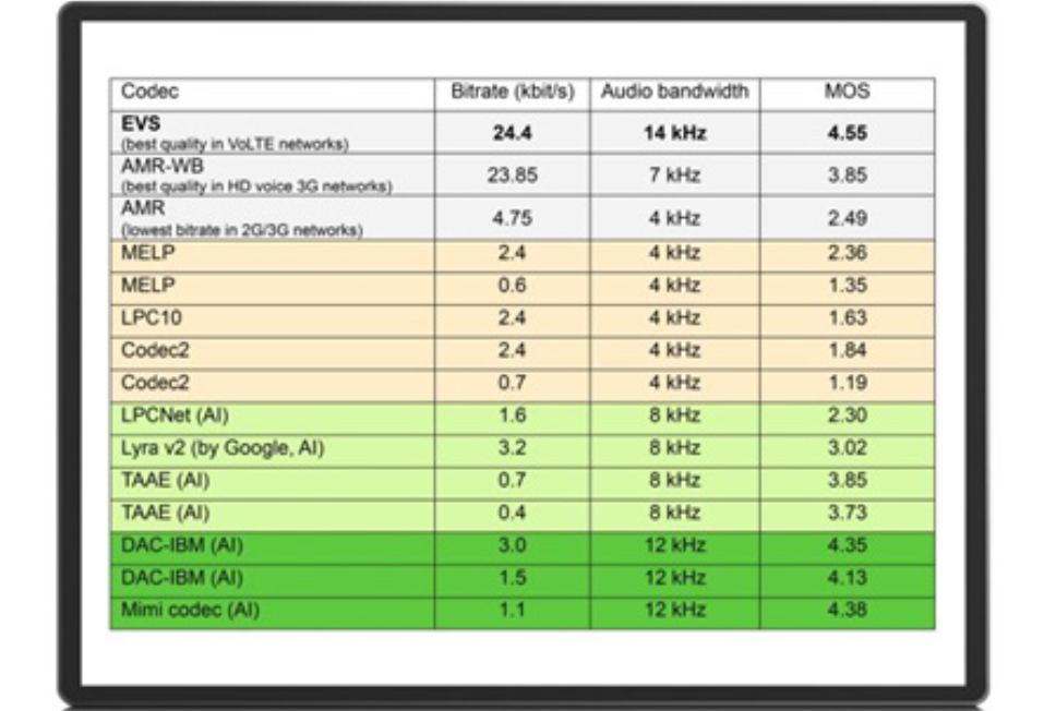
The following table shows some representative results of the listening experiment; the Mean Opinion Score (MOS) rates the subjectively perceived quality on a scale from 1 (bad) to 5 (excellent):
The detailed results of this evaluation, including statistical analysis, codec performance rankings, and listener feedback, are presented at the ITU-T SG12 meeting in September 2025. These insights are expected to contribute to ongoing discussions around codec standardisation, the definition of “quality,” and its automated prediction, particularly in the context of future mobile and satellite communication systems.
The post How good are ultra-low bitrate speech codecs? appeared first on ELE Times.
NXP CoreRide Puts Automakers on Fast Path to 48 V Scalable Zonal Architectures
NXP Semiconductors introduced its NXP CoreRide Z248 zonal reference system – the semiconductor industry’s first pre-validated, design-ready zonal foundation that combines advanced 48 V energy distribution, deterministic data handling, functional safety, and real-time responsiveness. The hardware-software foundation is designed to optimise system performance, reduce system integration effort, shorten development cycles, and allow OEMs and Tier 1s to focus investment where it matters most. It sets a new benchmark for accelerating the journey from zonal architecture concepts to production‑ready implementations.
Built on NXP’s S32K5 microcontroller series, its integrated advanced MRAM technology unlocks ultra-fast, ultra-frequent over-the-air updates throughout the entire vehicle lifecycle. At the software level, the Z248 integrates a comprehensive pre-validated software stack that streamlines complex development of smart data energy network (SDEN) functionalities such as impedance, power and protection monitoring, intelligent data routing, AI‑enabled virtual sensing, diagnostics, and audio.
With its built-in, validated remote protocol stack (RCP), it supports the up-integration of end node functions and ECU consolidation to enable new cost-optimised vehicle architectures. It also addresses key challenges of 48 V zonal systems by managing energy conversion, distribution, and protection within a single, integrated architecture.
The Z248 is rigorously validated through thousands of system-level tests demonstrating outstanding low-power modes, fast boot and fast wake-up response. It is supported by a modern, collaborative continuous integration, continuous testing and continuous delivery (CI/CT/CD) development environment that allows significantly faster test loops with OEMs and tier 1s, shortening validation cycles.
Why it matters: Automakers are being asked to move faster, scale broader, and spend smarter – even as safe zonal consolidation, hybrid power systems, and AI-enabled features dramatically increase architecture complexity. NXP’s new CoreRide zonal reference system brings scalability to this rising architectural complexity. It reduces risk by helping OEMs and tier 1s accelerate development into production, and it eases the switch from legacy platforms and lower total cost of ownership – freeing them from complex integration to put them on a path to production.
“As new E/E architectures redefine vehicle design, our focus is simple: give the automotive ecosystem the foundation to move faster and differentiate with confidence,” said Sébastien Clamagirand, SVP and General Manager, Automotive Systems & Platforms at NXP Semiconductors. “The NXP CoreRide zonal reference system Z248 delivers a performance-optimised, scalable 48 V foundation that intelligently fuses power, data and software, while dramatically simplifying system integration, reducing time to market, and enabling OEMs to focus on vehicle differentiation and long‑term value creation.”
More details: The Z248 zonal reference system is delivered with a complete Board Support Package (BSP) with pre-integrated software from the NXP CoreRide partner ecosystem, including GLIWA’s performance monitoring suite, Green Hills’ software compiler and Vector’s embedded software and tools. The full package undergoes extensive validation to help ensure optimised performance, while continuously improving processing efficiency and power consumption based on the primary use cases of a zonal ECU.
It’s a scalable, safe and secure hardware-software stack that adapts easily to different variants of SDV E/E architectures and integrates naturally with NXP’s broader system offering. It leverages technologies across computing, networking, power management and 48 V energy distribution, including NXP’s S32K566 zonal microcontroller featuring on-chip MRAM that significantly accelerates ECU programming times, both in factory settings and during over-the-air (OTA) updates.
The reference system also integrates 48‑volt‑capable power components such as eFuse, PMIC and DC‑DC converters, robust in‑vehicle networking through Ethernet PHY and CAN transceivers, and built-in audio support. In addition, it introduces a new concept for zonal I/O extension. Designed for broad applicability with housing and a wiring loom, the new NXP CoreRide Z248 zonal reference system can be deployed across ICE, hybrid and BEV platforms, supporting the industry’s move toward zonal processing and ECU consolidation.
Ecosystem Voices
Peter Gliwa, CEO and Founder of GLIWA
“NXP understood that the eco-system, the tooling around a new platform, is essential for its success. With our Analysis Suite T1 built into the NXP CoreRide Z248 zonal reference system, high efficiency, proper timing analysis and timing verification are very well addressed.”
Dan Mender, Vice President of Business Development at Green Hills Software
“Green Hills is proud to play a central role in NXP’s transformative reference solution strategy, which simplifies and accelerates production-focused automotive ECU development through pre-integrated hardware and software optimised for zonal automotive architectures. By leveraging Green Hills’ integrated software solutions, customers can develop high-quality, safety-critical applications with a minimal footprint and optimal performance, while significantly reducing time to deployment.”
Sam Yeh, Chairman of Inventec
“In response to the automotive E/E architecture trend toward zonal and centralised designs, Inventec is collaborating with NXP Semiconductors to support the advancement of next-generation zonal architectures. Through this collaboration, Inventec can provide hardware design and JDM support to OEMs as part of NXP’s zonal E/E architecture initiatives.”
Jochen Rein, Senior Vice President, Business Unit Software Platform at Vector
“The combination of the NXP CoreRide platform and Vector’s software foundation provides a robust basis for next‑generation zonal architectures. We enable our joint customers to reduce their time- to-market due to a pre-integrated and highly optimised software stack.” Vector contributes as an NXP CoreRide partner, providing pre‑integrated software and tools that help streamline development and ensure smooth integration within the zonal ECU architecture.”
The post NXP CoreRide Puts Automakers on Fast Path to 48 V Scalable Zonal Architectures appeared first on ELE Times.
Microchip Helps Manufacturers Meet Cybersecurity Regulations, Expands Security Services in the Trust Platform
The post Microchip Helps Manufacturers Meet Cybersecurity Regulations, Expands Security Services in the Trust Platform appeared first on ELE Times.
Everspin Launches New Generation of Unified Memory for Embedded Systems
Everspin Technologies, a leading developer and manufacturer of magnetoresistive random access memory (MRAM) persistent memory solutions, today announced the UNISYST MRAM family, a new generation of unified memory designed to fundamentally change how embedded systems store and access code and data.
“System designers are running into the physical and performance limits of NOR flash, especially as process nodes move below 40 nanometers and workloads become more demanding,” said Sanjeev Aggarwal, president and CEO of Everspin Technologies. “With UNISYST, we are extending our MRAM roadmap to higher densities while giving customers a practical way to start with PERSYST today and migrate to a code-and-data MRAM architecture as soon as it is available.”
UNISYST is a unified code-and-data MRAM architecture that bridges traditional configuration memory and higher-density persistent storage, extending MRAM into traditional NOR flash applications where superior performance, endurance and reliability are valued. Built as a natural extension of Everspin’s existing PERSYST MRAM platform, UNISYST gives customers a practical, simple migration path from today’s serial MRAM devices to higher-density unified memory without requiring changes to system architecture or software.
Everspin will initially offer the UNISYST family in densities ranging from 128 megabits to 2 gigabits, using a standard xSPI interface operating up to octal SPI at 200MHz. The devices are planned to feature AEC-Q100 Grade 1 qualification and minimum 10-year data retention at extreme temperatures, supporting demanding environments across automotive, aerospace, industrial and edge AI applications.
“As generative AI models move from the cloud to embedded systems, we’re suddenly dealing with assets that are tens or even hundreds of megabytes in size,” said Kwabena W. Agyeman, President and Co-founder of OpenMV. “Storing those models is only part of the challenge — updating them quickly during development and deployment is equally important. High-speed, non-volatile Everspin UNISYST MRAM changes what’s practical for edge AI systems by removing the write bottlenecks associated with traditional flash.”
UNISYST delivers high-bandwidth read and write speeds in a non-volatile memory device, enabling fast boot, rapid updates and predictable performance without the tradeoffs of traditional flash-based designs. By combining high-speed access with persistent storage, UNISYST supports software-defined systems that require frequent reconfiguration while maintaining data integrity across power cycles.
Everspin MRAM has been deployed in mission-critical storage applications for nearly two decades, valued for its endurance and reliability. UNISYST builds on Everspin’s proven MRAM foundation with capabilities designed to support more complex, software-defined systems:
- Code-and-data MRAM architecture designed as a next-generation alternative to other non-volatile memory
- Standard xSPI interface operating up to octal SPI at 200MHz
- Read bandwidth of up to 400 MB/s and write bandwidth of approximately 90 MB/s, over 400 times faster than NOR flash
- Write endurance up to 10 times higher than typical NOR
- AEC-Q100 Grade 1 qualification and minimum 10-year data retention for high-reliability designs
UNISYST is aimed at applications where non-volatile memory must combine high bandwidth, high endurance and predictable behaviour over temperature and time. Target use cases include:
- AI at the edge: Fast AI weight updates, critical storage at the edge, local code-and-data storage for workloads that need fast boot, rapid reconfiguration and non-volatile operation close to the sensor, with the ability to execute in place, removing the need for multiple system memories
- Military and aerospace: Field-programmable gate array (FPGA) configuration and code storage for mission-critical systems, including low-Earth orbit satellites and other platforms that require frequent over-the-air updates
- Automotive: Control, logging and configuration memory in systems that must meet Grade 1 temperature requirements and long-term data retention
- Industrial and casino gaming: High-traffic logging and configuration in environments that demand fast writes, long endurance and persistent storage supporting data logging
The launch of UNISYST represents a platform-level expansion of Everspin’s MRAM portfolio, extending the company’s role from a niche memory supplier to a mainstream memory player serving a multibillion-dollar market. By unifying code storage and data memory, Everspin is addressing the growing demands of software-defined systems that require faster boot times, frequent updates and predictable behaviour over long operating lifetimes.
The post Everspin Launches New Generation of Unified Memory for Embedded Systems appeared first on ELE Times.
TI’s microcontroller portfolio and software ecosystem expanded to enable edge AI in every device
Texas Instruments (TI) introduced two new microcontroller (MCU) families with edge artificial intelligence (AI) capabilities, supporting the company’s commitment to enabling edge AI across its entire embedded processing portfolio. The MSPM0G5187 and AM13Ex MCUs integrate TI’s TinyEngine neural processing unit (NPU), a dedicated hardware accelerator for MCUs that optimises deep learning inference operations to reduce latency and improve energy efficiency when processing at the edge.
TI’s embedded processing portfolio is supported by a comprehensive development ecosystem, including the CCStudio integrated development environment (IDE). Its generative AI features allow engineers to use simple language to accelerate code development, system configuration and debugging through industry-standard agents and models paired with TI data. Altogether, TI is accelerating the adoption of edge AI across electronic devices, from real-time monitoring in wearable health monitors and home circuit breakers to physical AI in humanoid robots. These end-to-end innovations are featured in TI’s booth at embedded world 2026, March 10-12, in Nuremberg, Germany.
“TI invented the digital signal processor almost 50 years ago, laying the groundwork for today’s edge AI processing,” said Amichai Ron, senior vice president, Embedded Processing and DLP® Products at TI. “Now TI is leading the next phase of innovation by integrating the TinyEngine NPU across our entire microcontroller portfolio, including general-purpose and high-performance, real-time MCUs. By enabling AI across our software, tools, devices and ecosystem, we are making edge AI accessible and easy to use for every customer and every application.”
“While much of the world has been focused on AI acceleration and NPUs in bigger SoCs, it turns out some of the more interesting and far-reaching applications of AI can be enabled inside smaller chips like microcontrollers,” said Bob O’Donnell, President and Chief Analyst at TECHnalysis Research. “Edge-based applications of AI acceleration can make consumer devices more intelligent and industrial devices more efficient. Plus, if you can combine these chips with software development tools that themselves leverage AI to help build AI features, you bring the power of AI acceleration to a significantly wider audience of engineers and device designers.”
Advanced intelligence at your fingertips
Consumers are always looking for everyday technology to be more intelligent, from fitness wearables to home appliances and electrical systems. However, many engineers believe that AI capabilities are limited to higher-end applications due to high costs, power demands, and coding requirements. TI’s new MSPM0G5187 Arm Cortex-M0+ MSPM0 MCU represents a fundamental shift for embedded designers, who can now bring edge AI to a wide range of simpler, smaller and more cost-effective applications.
With local computation, the TinyEngine NPU executes computations required by neural networks in parallel to the primary CPU running application code. Compared to similar MCUs without an accelerator, this hardware acceleration:
- Minimises the flash memory footprint.
- Lowers latency by up to 90 times per AI inference.
- Reduces energy utilisation by more than 120 times per AI inference.
Such levels of efficiency allow resource-constrained devices – including portable, battery-powered products – to process AI workloads. At under US$1 in 1,000-unit quantities, the MSPM0G5187 MCU reduces system and operating costs by offering an affordable alternative to other MCU or processor architectures.
Real-time control plus AI acceleration for multimotor systems
Motor control applications in appliances, robotics and industrial systems increasingly call for intelligent features such as adaptive control and predictive maintenance, but implementing these capabilities has historically required complex, multi-chip designs. Building on over two decades of motor control leadership through the C2000 real-time MCU portfolio, TI’s new AM13Ex MCUs are the industry’s first to integrate a high-performance Arm Cortex-M33 core, TinyEngine NPU and advanced real-time control architecture into a single chip.
This degree of integration enables designers to implement sophisticated motor control and AI features simultaneously without external components, lowering bill-of-materials costs by up to 30%. Key enhancements include:
- The ability to maintain precise real-time control loops for up to four motors while the TinyEngine NPU runs adaptive control algorithms for load sensing and energy optimisation.
- An integrated trigonometric math accelerator that performs calculations 10 times faster than coordinate rotation digital computer (CORDIC) implementations, delivering more precise, responsive motor-control performance.
Easily train, optimise and deploy AI models
Both MCU families are supported by TI’s CCStudio Edge AI Studio, a free development environment that simplifies model selection, training and deployment across TI’s embedded processing portfolio. This edge AI toolchain gives engineers full flexibility to run AI models on TI MCUs through either hardware or software implementations. Today, there are more than 60 models and application examples available in the tool to help developers start deploying edge AI in any device, with additional tasks and models planned in the future.
The post TI’s microcontroller portfolio and software ecosystem expanded to enable edge AI in every device appeared first on ELE Times.
R&S to showcase future-proof EMC testing solutions at EMV 2026
Rohde & Schwarz will participate in EMV 2026, Europe’s premier trade fair and congress dedicated to electromagnetic compatibility, held from March 24-26 in Cologne. At the event, which serves as a crucial platform for industry professionals, the company will show its latest advancements in test & measurement equipment to address the evolving challenges within the EMC landscape.
Rohde & Schwarz will demonstrate a broad portfolio of solutions designed to streamline and optimise EMC testing across diverse sectors, including power electronics, consumer, industrial, automotive, Satcom, military, and wireless communications. EMC testing is evolving to meet the demands of emerging technologies and a crowded radio frequency spectrum. Innovations like AI, 6G, and quantum computing present new challenges for ensuring reliable performance, while widespread electrification and increased bandwidth requirements necessitate testing at higher frequencies. To address these shifts, Rohde & Schwarz is developing scalable and modular test solutions focused on repeatable, reliable measurements – streamlining the path from initial assessment to final certification. A further focus is on bridging the gap between real-world field performance and laboratory testing.
At the show, Rohde & Schwarz will showcase a versatile and adaptable solution for conducted and radiated emission testing with the EMI test receivers R&S EPL1001 and R&S EPL1007 with frequency ranges up to 1 GHz and 7.125 GHz. These receivers provide a scalable approach to EMC testing, allowing users to select the optimal configuration for their needs, whether for efficient pre-compliance measurements or fully CISPR 16-1-1 compliant testing for certification.
Rohde & Schwarz is showcasing a speed-optimised EMI test with its industry-leading R&S ESW test receiver — with ESW-B1000R 970 MHz bandwidth extension — and the automated R&S ELEKTRA software: A live demonstration highlights the system’s capabilities for rapid and detailed device characterisation with 3D emission plots generated by R&S ELEKTRA for a typical commercial EMI test. Complementing this is the R&S HF1444G14 high-gain antenna, extending testing capabilities up to 44 GHz for standards like MIL-STD and FCC.
Rohde & Schwarz will also be expanding its R&S BBA300 family of broadband amplifiers with its new dual-band amplifier series R&S BBA300-CDE/FG for 380 MHz to 13 or 18 GHz and the R&S BBA300-DE1000 with an output power of up to 1000 W in the 1 GHz to 6 GHz range. With high linearity, continuous and very wide frequency bands, and innovative protection concepts for high availability, the R&S BBA300 family meets the requirements for EMC immunity testing today and tomorrow.
Rohde & Schwarz will also show its full vehicle antenna test (FVAT) capabilities at the show. Modern vehicles increasingly rely on multiple antennas – for GNSS, Wi-Fi, cellular services like C-V2X, and more to enable safety, convenience and infotainment features – requiring comprehensive full-vehicle antenna testing. This testing enables vehicle manufacturers and their suppliers to characterise radiation performance, verify RF robustness, ensure co-existence of different wireless technologies and ultimately validate the functions and services enabled by wireless connectivity.
For in-depth signal analysis, Rohde & Schwarz will feature the R&S MXO 3 Series oscilloscope, boasting an unmatched acquisition rate exceeding 4.5 million waveforms per second and featuring up to 8 channels. This advanced oscilloscope also includes powerful standard functions such as a very fast FFT and zone trigger capabilities that empower engineers to quickly and precisely understand complex circuit behaviour, essential for effective EMI troubleshooting and design optimisation.
Rohde & Schwarz will also actively contribute to the congress with technical sessions, workshops and demos focusing on EMI test speed optimisation, EMC for medical products and closed-loop Reverb chamber testing. Attendees can also join a panel discussion exploring the impact of Artificial Intelligence on the EMC landscape, covering its current benefits and potential future challenges. Besides others, a Rohde & Schwarz expert will discuss AI’s role in areas like testing and development, and address concerns about new vulnerabilities.
The post R&S to showcase future-proof EMC testing solutions at EMV 2026 appeared first on ELE Times.
Infineon extends leadership position in global microcontroller market
Infineon Technologies further extends its number one position in the global microcontroller market. According to the latest research by Omdia [1], the company increased its total microcontroller market share to 23.2 per cent in 2025 (2024: 21.4 per cent), achieving a year-on-year gain of 1.8 percentage points – the largest increase among its competitors. Notably, this market share gain was achieved against the backdrop of a slightly declining microcontroller market (-0.3 percent).
“This great market result reflects our relentless commitment to accelerating innovation for customer value, outstanding system solutions, and strong customer relations,” said Andreas Urschitz, Chief Marketing Officer and Member of the Management Board at Infineon. “With our superior product portfolio, reliable software, and easy-to-use development tools, we help our customers create value and address the global challenges of decarbonization and digitalisation. Outgrowing the market is a direct outcome of our continued investment in technology and our close collaboration with our partners worldwide.”
Ethernet to enhance microcontroller business for software-defined vehicles
Infineon climbed to the top spot in the global microcontroller market for the first time in 2024, after becoming the number one in the specific market for automotive microcontrollers already one year earlier. The company’s leading market position will be further strengthened by the successful acquisition of Marvell’s Automotive Ethernet business, a milestone transaction completed in August 2025. This move expands Infineon’s cutting‑edge connectivity portfolio, enhancing the company’s system capabilities for central compute architectures in software-defined vehicles (SDV). Integrating the industry-leading BRIGHTLANE automotive Ethernet portfolio with Infineon’s AURIX, PSOC and TRAVEO automotive microcontroller families creates an unmatched system offering for SDVs, enabling features such as autonomous driving, advanced driver‑assistance systems, and secured over‑the‑air updates.
Infineon microcontrollers empower physical AI, such as humanoid robots
Furthermore, the acquisition opens additional growth opportunities in emerging IoT fields and physical AI, such as humanoid robotics. AURIX, PSOC and MOTIX microcontrollers from Infineon empower humanoid robots to safely perceive, think, and interact with their environment in real-time, facilitating advanced computing, smart actuation and motor control, connectivity, and intelligent edge functions.
Infineon enables the key functional blocks in humanoid robots, supporting customers from concept to mass production across industrial, service, and home applications. With its PSOC portfolio, Infineon continues to expand its presence in industrial and consumer markets, offering scalable, secure, and power‑efficient microcontroller solutions widely used in smart home systems, industrial control equipment and connected IoT devices.
Cybersecurity features for future requirements are already implemented today
From IoT devices to connected vehicles, industrial infrastructure, AI‑driven applications, and robotics, cybersecurity is essential. Therefore, Infineon microcontrollers are engineered with future-proof security in mind to protect data, identities and systems from the start and across the entire lifecycle. This includes, for example, complying with international security standards such as ISO/SAE 21434 (automotive security) for the latest generation AURIX and TRAVEO MCUs. Furthermore, Infineon engineers architectures that meet future requirements, such as from the EU Cyber Resilience Act or for post-quantum cryptography, already today – for example, in the latest PSOC products for industrial and consumer applications, as well as AURIX and TRAVEO automotive MCUs.
Infineon at embedded world 2026: Showcasing future-ready innovations
From 10 to 12 March 2026, at embedded world in Nuremberg, Germany, Infineon is presenting its comprehensive portfolio of industrial, consumer and automotive microcontrollers, with a strong focus on innovation for secured, connected, and intelligent systems. Visitors can experience this at Infineon’s booth (Hall 4A, Booth 138) and through a series of presentations and live demos.
[1] Based on or includes research from Omdia: Annual 2001-2025 Semiconductor Market Share Competitive Landscaping Tool – 4Q25. March 2026. Results are not an endorsement of Infineon Technologies AG. Any reliance on these results is at the third party’s own risk.
The post Infineon extends leadership position in global microcontroller market appeared first on ELE Times.
Traction Inverter: Keys to understanding the inverter, the traction, and why X-in-1 solutions are increasingly popular
Courtesy: STMicroelectronics
Traction inverters are at the heart of electric vehicles, meaning that they are one of the modules with the most significant impact on overall efficiency, range, and performance. According to the US Department of Energy, the electric drive system is responsible for some of the most significant losses in an EV, totalling about 18%. Moreover, a report by McKinsey & Company explains that the “top reasons” for consumers to avoid EVs are costs, charging concerns, and range anxiety, two of which are mainly impacted by the traction inverter’s performance. Optimising the electric drive train is thus the quickest and surest way to improve an EV to make it more compelling, and why ST recently published a white paper on traction inverters
Why are traction inverters challenging? The role of a traction inverter A traction inverter
In a nutshell, the traction inverter takes the DC electrical energy from the battery, converts it into properly commutated three-phase alternating current, and sends it to a traction motor, which then converts it into kinetic energy. Consequently, the traction inverter is also responsible for modulating the AC sent to the motors to adjust for things like torque and speed. Similarly, regenerative braking, which converts mechanical energy into DC power to recharge the battery, also depends on the traction inverter. Hence, the reason drivers love the responsiveness of their EVs, as well as how certain driving features can extend the overall range, is dependent on the performance of the traction inverter, among other things.
The challenges behind the traction and the inversion A DC-DC Converter
While most two-wheel-drive vehicles will have one or two inverters, an all-wheel drive may have up to one inverter per traction motor and one traction motor per wheel. It all depends on how car makers want to address the car’s overall performance. Hence, it’s easy to see some of the challenges that engineers must solve when designing a traction inverter that must not only convert electrical energy but also sense phase current, monitor motor position, and even manage control loops. While many engineers focus on the “inverter”, “traction” comes with a unique set of challenges, such as determining a rotor’s position with precision, or the whole traction inverter will be grossly inefficient.
Moreover, as EVs increasingly support high-power DC charging, they come with higher DC-link voltages, which means the traction inverter must adapt to reduce losses while enabling traction motors to draw more power. It’s a great example of how modern car modules are highly interdependent and how changing one aspect of the vehicle has ripple effects on many other systems and modules. As the white paper shows (see Table 3), there’s a strong “correlation between motor power, battery size, and DC link voltage.” Put simply, engineers can’t design traction inverters in isolation but must take a more global approach or risk seriously hampering performance due to a poorly suited system.
How to find solutions and design great traction inverters? Choosing the right gate driversTo answer these challenges, the white paper aims to provide key concepts and solutions engineers can apply to their designs. For instance, it looks at how to use gate drivers and power transistors to modulate the current in stator windings. Too often, teams treat these devices as commodities and miss the critical impact they may have on their traction inverters. However, a mismatch between the transistors and gate drivers will result in significantly higher losses, among other things. It’s why a galvanically isolated driver for IGBT and SiC MOSFETs, like the STGAP4S, can make a tremendous difference. ST even offers an evaluation board, the EVALSTGAP4S, which significantly hastens the development of a proof of concept.
Finding the right microcontroller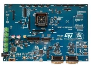 The SR5E1-EVBE5000P
Another challenge is the ability to control the traction motors with enough precision and speed to improve the EV’s performance. Such a feat is directly tied to the microcontroller that will house the PWM timers and the logic responsible for calculating the field-oriented control mechanisms, among other functions. Using the wrong device will not only hinder performance but also create critical problems that cannot be fixed easily unless the platform supports things like over-the-air updates, the highest levels of functional safety, and more. ST is already offering MCUs tailored for EV applications, like the new Stellar E series and evaluation boards like the SR5E1-EVBE5000P.
Adopting the X-in-1 trendAnd the white paper contains so many more solutions, tips, and expert advice. As ST offers a unique and wide-ranging portfolio of devices that can directly improve traction inverters, the paper also helps engineers anticipate a new trend: X-in-1. Increasingly, we see makers coming up with integrated systems that include the on-board charger, DC-DC converter, and traction inverter. Since these systems impact one another, integrating them helps create a more meaningful and intentional design. However, that means engineers must widen their expertise and rely on a portfolio that includes a broader range of devices.
The post Traction Inverter: Keys to understanding the inverter, the traction, and why X-in-1 solutions are increasingly popular appeared first on ELE Times.
5 Upcoming AIoT Trends to Lookout for in 2026
Courtesy: Hikvision
As we enter 2026, the convergence of artificial intelligence (AI) and IoT infrastructure is reshaping industries, unlocking unprecedented opportunities to optimise operations, enhance security, and improve sustainability. Yet with great technological power comes great responsibility, and the AIoT industry is increasingly focused on ensuring AI develops in ways that are safe, ethical, and beneficial to all. Here are the five key trends shaping the AIoT landscape in 2026.
Scenario-based AIoT solutions are rapidly unlocking new business valueThanks to AIoT, we are witnessing a profound digital shift moving beyond basic IT informatisation to deep integration with Operational Technology (OT). In this transition, business value is no longer created by fragmented data collection, but increasingly by harvesting insights naturally and continuously from daily operations. By embedding perception capabilities into specific real-world scenarios, AIoT is enabling organisations to move from manual management to much more agile, automated control.
This is creating operational capabilities that were once impossible, enabling real-time decision-making, which can rapidly deliver new business value. In the field of industrial safety, for example, we see workshops shifting from reactive response to proactive prevention. Hazardous manual inspections are being replaced by advanced spectral technologies such as TDLAS, which remotely detect natural gas leaks in seconds. The result is a dramatic reduction in response times to emergency situations.
It’s a similar story with quality control. Food manufacturers, for example, are now leveraging AI-driven X-ray systems to instantly identify foreign objects like stones, glass, and bone that were once invisible.
Or consider inventory management, where mining and feed plants are now utilising 3D millimetre-wave radar to automatically scan silos. This is yet another application of AIoT that, in this case, is creating a new level of precision in volumetric data, eliminating human error, and enabling fully automated, real-time control.
Large-scale AI models are evolving into new capabilities for “AI+”Large-scale AI models are empowering the core analysis and processing flow through “AI+” integration. While large language models have revolutionised human-digital interaction, industry-specific models are now reshaping how IoT data interacts with the physical world.
We can already see that by embedding AI into data analysis and signal processing, these models significantly enhance precision and efficiency. For example, traffic and perimeter security models, trained on massive datasets, are pushing the limits of perception. By processing complex data, they minimise false alarm rates for incidents and intrusions. Meanwhile, in audio sensing, “AI+ signal processing” is redefining audio capture by filtering background static and isolating human voices in noisy environments. This technology improves the signal-to-noise ratio, ensuring clear sound pickup even in challenging conditions.

Deeply anchored in this multi-modal understanding, AI Agents are now bridging the gap between perception and human intent. Powered by large language models, these agents enable users to communicate naturally using everyday language. Commands like “Find the person wearing purple clothes who parked a blue SUV this morning” are processed by intelligent security systems to automatically retrieve relevant video segments. Such capabilities are transforming AIoT systems from specialised tools that require professional training into intelligent assistants that are accessible to everyone.
Edge AI is transforming devices from data collectors to intelligent analysersAnother shift we are seeing is towards edge computing. Increasingly, the “Cloud + AI” model is no longer the only option for enterprise digitalisation. By moving AI functions from the cloud to the edge, organisations can achieve millisecond-level response times, operate seamlessly offline, and maintain on-premises privacy. It’s an architectural shift that eliminates bandwidth dependency and significantly reduces infrastructure overhead.
Because devices process raw data directly, this localised architecture extends its value by greatly optimising storage efficiency. This is particularly significant for complex video analysis, powered by visual AI models. Here, edge devices can now precisely identify key targets such as people or vehicles at the source. Based on this accurate segmentation, the system applies differentiated encoding—preserving critical foreground details, while compressing background areas that contribute little investigative value.
This AI-driven approach drastically reduces storage requirements without sacrificing visual clarity. For organisations deploying thousands of cameras across multiple sites, this naturally translates into substantial savings on storage infrastructure, lower ongoing costs, and simplified data management, making large-scale AIoT deployments economically viable.
Responsible AI is embedding ethics into every stage of innovationAI is transforming our lives, work, and business at an unprecedented pace. Yet, this revolution brings a critical responsibility: to ensure innovation unfolds safely, ethically, transparently, and beneficially for all. Responsible AI is no longer optional—it is both a moral imperative and a strategic necessity that builds trust, mitigates risk, and drives long-term innovation. As public awareness and regulatory oversight intensify globally, from Europe’s regulatory pioneering to regional initiatives worldwide, international collaboration becomes essential to harnessing AI’s potential while, at the same time, promoting security, prosperity, and human well-being.

Responsible AI practices, then, must permeate the entire AI lifecycle—from research and development to deployment and real-world application.
This includes establishing guiding principles and governance frameworks, adopting responsible approaches throughout development, and ensuring safety, accountability, and transparency in products and solutions. It is a systematic endeavour requiring industry-wide coordination and collective action across sectors and borders, involving policymakers, industry partners, researchers, and other stakeholders. Only through sustained commitment and open collaboration can we shape an AI future that truly serves humanity.
AIoT is expanding technology’s role from business to society and the environmentAnother key trend that we are seeing is the rapid expansion of application areas for AIoT. In addition to the traditional business solutions, AIoT is now being widely adopted for broader social and environmental applications, demonstrating how intelligent systems can serve humanity and nature.

In ecological protection, for example, specialised AIoT devices are revolutionising conservation efforts, from wildlife monitoring to vegetation health tracking. Indeed, crop growth monitoring systems that leverage AIoT technologies for large-scale, real-time analysis of crop health are becoming increasingly widespread in agriculture. This capability addresses the inefficiencies of manual inspections, enabling precise management and optimising yields through digitisation.
AIoT is also being used to improve public safety. AI-driven drowning prevention systems, for example, are being deployed in areas which are known to be high risk. They utilise real-time video analytics to detect hazardous conditions, automatically identifying when an individual enters dangerous areas, for example. When this happens, the technology triggers an immediate alert, transforming passive monitoring (or no monitoring at all) into a highly effective and proactive solution that can save lives.
Looking ahead: the future of AIoTFor organisations accelerating their digital transformation journeys, these trends offer both guidance and inspiration. The future of AIoT, after all, is about creating real value for businesses, enhancing experiences for people, and building a more sustainable world for everyone. And that future is arriving now.
The post 5 Upcoming AIoT Trends to Lookout for in 2026 appeared first on ELE Times.
Space internet is coming, and satellite networks could bypass app stores and telcos entirely
Low Earth Orbit (LEO) satellite constellations are entering a new phase of telecom relevance. What began as fixed satellite broadband for remote homes has evolved into direct-to-device connectivity integrated within 3GPP Non-Terrestrial Network standards. Modern satellites are no longer simple bent-pipe relays. They incorporate regenerative payloads, digital beamforming arrays, onboard processing, and inter-satellite optical links that allow orbital mesh routing. The engineering sophistication is undeniable.
However, for telecom professionals and network architects, the key discussion is not about technological capability. It is about architectural positioning: can satellite networks scale to rival terrestrial radio access networks (RAN)? Can they bypass traditional telecom operators? And do they meaningfully challenge app-store ecosystems? The answers require a grounded understanding of spectrum physics, link budgets, and capacity density.
Spectrum Architecture: IMT and Non-IMT Realities
Direct-to-device satellite systems operate either in traditional satellite allocations (non-IMT bands such as L-band or S-band) or within IMT spectrum harmonised under 3GPP NTN specifications.
In non-IMT bands, scalability faces structural limits. Propagation at these frequencies is highly dependent on near line-of-sight conditions. Building penetration loss, urban canyon multipath fading, and foliage attenuation reduce reliability. Unlike terrestrial networks that can densify through small cells and sectorization, satellites illuminate wide geographic footprints. They cannot dynamically increase cell density in obstructed urban terrain.
This makes non-IMT direct-to-handset connectivity better suited for open environments such as rural regions, highways, maritime routes, and disaster zones rather than dense urban centres. IMT integration under NTN introduces greater harmonisation. Release 17 and beyond specify extended timing advance calibration, Doppler shift compensation, modified Hybrid Automatic Repeat Request (HARQ) timing, and satellite-aware mobility management. Devices can theoretically switch between terrestrial LTE/5G and orbital access with protocol continuity.
Yet the operational model remains conditional. Satellite access is typically triggered when terrestrial RSRP or SINR drops below defined thresholds. The modem evaluates signal quality and only activates NTN mode when necessary. This ensures satellite resources are preserved, and terrestrial networks handle high-density traffic loads.
Elon Musk, CEO of SpaceX, captured the strategic goal succinctly:
“There should be no dead zones anywhere in the world for your cell phone.” The emphasis is on coverage ubiquity, not urban capacity replacement.
Capacity Density: The Defining Constraint
The most decisive technical limitation is spectral density. Terrestrial operators achieve massive throughput through:
- Massive MIMO spatial multiplexing
- Dense macro-cell grids
- Small-cell layering in high-traffic zones
- Fibre-backed backhaul
- Millimeter-wave overlays
- Aggressive frequency reuse patterns
Satellite beams, even with advanced spot-beam architectures and frequency reuse, cover substantially larger areas. The spectral efficiency per square kilometre cannot match dense terrestrial deployments. Additionally, handheld devices operate under strict uplink power constraints, limiting achievable modulation and coding schemes for satellite links.
From a Shannon capacity standpoint, satellite systems are optimised for wide-area coverage, not high-density concurrency. In densely populated markets, even a mid-sized terrestrial operator can deliver greater aggregate throughput than an orbital beam serving the same footprint. This reality defines satellite’s optimal roles:
- Extending connectivity to underserved geographies
- Providing redundancy during disasters
- Supporting maritime and aviation mobility
- Enabling IoT in sparse environments
- Enhancing national connectivity resilience
Gwynne Shotwell, President of SpaceX, has consistently emphasised connectivity as foundational infrastructure. Reliable global access enables economic participation in regions where terrestrial networks are economically infeasible. The engineering model aligns with that vision.
Inter-Satellite Routing and Cloud-Native Architecture
Modern LEO constellations differentiate themselves through inter-satellite optical links (ISLs). Instead of routing traffic exclusively through ground gateways, data can hop between satellites before downlinking closer to its destination. This reduces dependence on terrestrial fibre choke points and can optimise long-haul routing paths.
Software-defined payloads further allow dynamic beam shaping, adaptive spectrum allocation, and load balancing. Combined with cloud-native packet cores and virtualised network functions, satellite systems increasingly resemble distributed edge clouds in orbit.
However, engineering challenges persist:
- Beam handover must be predictive to prevent session drops.
- Doppler shift compensation requires continuous frequency correction.
- Latency variability introduces jitter that must be absorbed at the transport layer.
- Congestion control algorithms, often QUIC-based, must adapt dynamically.
These are solvable challenges, but they reinforce the reality that satellite networks are engineered for resilience and reach rather than metro throughput supremacy.
Application Distribution and App-Store Dynamics
The notion that satellite networks could bypass app stores often conflates connectivity with runtime control. Satellite networks can facilitate cloud-streamed applications, Progressive Web Apps leveraging Web Assembly, multicast firmware updates, and enterprise-managed OTA deployments. However, runtime enforcement remains device-governed. Operating systems from Apple and Google maintain secure boot chains, code-signing validation, and hardware root-of-trust mechanisms independent of the access network.
Thus, while connectivity may be decentralised, execution control remains centralised within device ecosystems. App-store displacement at mass consumer scale remains unlikely in the near term. Satellite-enabled distribution is most viable in enterprise, industrial, defence, and controlled-device environments where policy governance is internally managed.
Global Regulatory Architecture
Satellite beams inherently traverse national borders. This introduces complex regulatory questions regarding lawful intercept, spectrum harmonisation, emergency service prioritisation, and data sovereignty. Unlike terrestrial towers confined within licensed areas, orbital coverage footprints overlap multiple jurisdictions simultaneously.
Regulators worldwide are converging toward coexistence frameworks where satellite operators must comply with local licensing, security audits, and traffic monitoring obligations. Encryption policies, gateway localisation requirements, and national security clearances are increasingly embedded within approval processes.
Indian Regulatory Perspective
In India, satellite internet operates within a structured licensing regime under the Department of Telecommunications. Operators must obtain a Global Mobile Personal Communication by Satellite (GMPCS) license to provide satellite communication services. Spectrum allocation is subject to administrative assignment or auction-based frameworks, depending on policy direction. Gateway earth stations require approval from national authorities, and security compliance is mandatory. Traffic monitoring capabilities must be provisioned in accordance with lawful intercept regulations. Data localisation considerations, especially under emerging digital governance frameworks, may require traffic breakout within Indian jurisdiction rather than pure inter-satellite routing for domestic data flows.
Additionally, satellite services must align with spectrum coordination under the Wireless Planning & Coordination (WPC) Wing. Coexistence with terrestrial IMT networks requires careful interference management and harmonisation. Regulatory approvals also involve security vetting of network elements and equipment supply chains.
India’s regulatory approach emphasises sovereign oversight while encouraging innovation through hybrid terrestrial-satellite integration models. Partnerships between satellite operators and domestic telecom providers are often preferred to ensure compliance with national security and licensing frameworks.
Industry Alignment: Complement, Not Replace
Sunil Bharti Mittal, Chairman of Bharti Airtel, has emphasised cooperation between satellite and terrestrial operators. In dense markets, terrestrial RAN grids remain unmatched in spectral reuse efficiency and urban throughput.
The long-term architecture, therefore, becomes hybrid:
- Terrestrial networks manage dense capacity loads.
- Satellite networks eliminate coverage gaps.
- Multi-RAT device logic dynamically orchestrates between both.
This convergence is not theoretical. It is already embedded within modem firmware design, NTN standardisation, and regulatory frameworks.
Engineering Takeaways
Telecom engineers and policymakers should focus on:
- Intelligent multi-RAT orchestration between terrestrial and NTN layers
- Adaptive transport protocols for variable-latency satellite links
- Robust cryptographic identity frameworks for secure OTA distribution
- Spectrum coexistence planning in IMT-integrated NTN deployments
- Regulatory compliance mechanisms for cross-border satellite beams
Conclusion
Space internet is a meaningful technological evolution. Advanced beamforming, regenerative payloads, inter-satellite optical routing, and NTN standardisation represent major engineering progress. But spectrum reuse laws and capacity density constraints remain decisive. Satellite networks excel in reach, resilience, and redundancy. Terrestrial networks dominate high-density throughput and urban spectral efficiency. The future of connectivity is not orbital disruption of telecom operators or wholesale bypass of app ecosystems. It is a structured convergence of a layered architecture where Earth and orbit operate in coordinated harmony.
Engineers who design seamless integration across these layers will define the next decade of global communications.
The post Space internet is coming, and satellite networks could bypass app stores and telcos entirely appeared first on ELE Times.
Motor Vehicle Motors Without Rare Earths: Chara Technologies’ Reluctance Motor Bet
Six years ago, when rare earth magnets were still a footnote in most mobility conversations, Bhaktha Keshavachar was already convinced they would become a problem. “We are going from hydrocarbons to electrons for all of our energy,” says the Co-Founder and CEO of Chara Technologies in an exclusive interaction with Kumar Harshit, Technology Correspondent, ELE Times. “In this electric future, motors will be at the heart of every machine. They will be the engines of the future economy. And if motors are central, they must be sustainable.”
At the time, Permanent Magnet Synchronous Motors (PMSMs) dominated electric mobility. Efficient, compact, and powerful, they owed much of their performance to neodymium-iron-boron magnets—magnets built on rare earth elements. But to Bhaktha, the efficiency narrative hid a deeper vulnerability.“One country controls 90 to 95 per cent of the rare earth supply chain,” he says. “It’s not about whether that country is good or bad. They will do what is in their best interest. But that may not be good for us.”
That asymmetry, coupled with environmentally intensive mining and rising geopolitical tensions, became the trigger. “Rare earth is a global problem. Everyone is experiencing the same issue. If we build the right product, the opportunity is global.”
Rethinking the MotorTo understand Chara’s bet, one must first understand how conventional motors work. In a PMSM, the stator generates a rotating magnetic field. The rotor, embedded with powerful permanent magnets, locks onto this field, producing torque. “It works really well,” Bhaktha acknowledges. “The magnets help generate larger torque for smaller amounts of current.”
Induction motors avoid magnets but sacrifice efficiency and power density in traction applications. That left a third architecture—reluctance motors. “The principle is simple,” he explains. “Magnetic flux always takes the path of least resistance. Just like water. Our rotor is designed so that it constantly tries to align itself to the lowest reluctance path. That alignment generates torque.”
Instead of relying on embedded magnets, Chara’s motor uses precisely engineered electrical steel geometries. “We depend on the properties of electrical steel to generate torque. That is the source of its simplicity.” Physics is not new. The engineering to make it commercially competitive is.
The Trade-Off No One SeesRemoving magnets means giving up their brute magnetic strength. To compensate, Chara increases copper in the windings and optimises steel design. The result is a motor that is roughly 15 per cent heavier than a comparable PMSM.
“Our most popular motor is for a three-wheeler,” Bhaktha says. “A PMSM motor is about 15 kilograms. Ours is about 18 kilograms.” On paper, that sounds like a disadvantage. But Bhaktha shifts the conversation from component-level comparison to system-level thinking.
“In a three-wheeler with a gross vehicle weight of 750 kilograms, three kilograms is a rounding error,” he says. “But efficiency over the duty cycle is what really determines range.” He explains how PMSMs require flux weakening at higher speeds—injecting additional current to counteract the very magnets that give them low-speed torque. That process consumes energy and complicates control.
“Our efficiency curve is flatter,” he says. “In duty cycle efficiency, we are 5 to 10 per cent better. For the same vehicle and same battery, you can get 5 to 10 per cent more range.” That improvement can eliminate the need for additional battery capacity—often heavier and costlier than the motor difference itself. “At the system level, our motor can actually make the vehicle lighter,” he adds.
From Scepticism to ShipmentsAfter four years of R&D, Chara began commercial sales in 2024. Today, it ships hundreds of motors every month to customers in India and abroad. But market acceptance did not come easily. “Three questions were always asked,” Bhaktha recalls. “‘Where have you deployed this? What about long-term reliability? And how can we depend on a startup?”
Convincing OEMs to replace the “heart of the machine” with a new architecture required more than performance claims. It required patience—and, unexpectedly, geopolitics. “Only after the geopolitical eruption last year did people start seriously looking at our technology,” he says. “Business improved a lot after that.”
The rare earth issue, once dismissed as distant, had become immediate.
Longevity Without MagnetsReliability is often framed as a risk for new technologies. Bhaktha turns that assumption around. “If you put everything on equal footing, induction motors and our motors should actually have longer life,” he explains. “Permanent magnets can demagnetise because of temperature or external fields. We don’t have that problem.”
By eliminating magnets from the rotor, the design removes a potential failure mode altogether. “In terms of reliability, we are equal or better than PMSM,” he says.
India’s Strategic MomentThe conversation inevitably widens to India’s industrial landscape. Electronics assembly is growing. Semiconductor fabs are emerging. Government schemes like the Electronic Component Manufacturing Scheme (ECMS) are pushing localisation.
“The controller part of the motor is electronics,” Bhaktha notes. “Schemes like ECMS will definitely help. We need that support. It’s like a child learning to walk—the initial support matters.” While motor materials such as steel and copper are already sourced domestically, semiconductor components remain largely import-dependent. “We have to start a strategic drive for components,” he says. “Otherwise, we will face the same vulnerability elsewhere.”
China’s dominance across the value chain looms large in his assessment. “In cost, quality, and timeliness, it is very hard to beat them today,” he says candidly. “But India has a large domestic market. We can deploy new technologies here, nurture them, and then export.”
Capital, Talent, and ConvictionBuilding deep-tech hardware in India is not easy. “Capital is scarce for projects like us,” Bhaktha says. “Our gestation periods are long. We need patient capital that can wait ten or fifteen years.” Talent, too, presents challenges. “It is easier to find people who write software code than people who understand electromagnetics, thermals, and hardware,” he says. But a reverse migration trend is helping. Engineers trained at global universities are returning, drawn by the opportunity to build foundational technologies.
And then there is the storytelling. “It was very difficult to explain why we were doing this,” he admits. “Rare earth was not even a mainstream phrase when we started.”
The 2030 MixBhaktha does not predict a single architecture winning the future. Instead, he envisions a diversified market. “Just like we had petrol, diesel, and CNG engines, we will have PMSM, reluctance motors, externally excited synchronous motors, and induction motors,” he says.
In traction applications alone, he believes rare-earth-free motors could capture about a quarter of the market by 2030. “It might be more,” he adds. “It is difficult to predict how quickly these things move. But rare earth is a real problem. As long as we keep solving the right problem, there will be opportunities.”
Conclusion
The electric revolution is often framed as a battery story. But as Bhaktha reminds us, every electron must eventually turn a shaft. If that shaft can spin without strategic dependencies embedded inside it, the implications extend far beyond efficiency. They touch resilience, sovereignty, and industrial autonomy.
Rare earth-free motors, once a niche research topic, are now entering production lines. And in that shift lies a quiet redefinition of what powers the electric future.
The post Motor Vehicle Motors Without Rare Earths: Chara Technologies’ Reluctance Motor Bet appeared first on ELE Times.
Photonics-electronics Convergence Technology Becomes Essential to Next-generation DCs Precise Measurements Required for DCI Evaluation
Courtesy: Anritsu Corporation
Due to the capacity constraints imposed by metropolitan areas, there is a growing trend to shift towards decentralized regional data centers. Along with the adoption of optical coherent transmission, such as 400G-ZR and OpenZR+, key to achieving this is the precise visualisation of fine quality. Anritsu, a long-established manufacturer of measurement instruments, supports this advancement of data centre networks with its high-precision measurement technology and support system completed in Japan.
The rapid growth in demand for AI has accelerated the global development of data centres, giving rise to an explosive growth in the amount of computational processing. In Japan, however, capacity limits are becoming apparent due to there being little physical space and an overextended electricity grid in metropolitan areas such as Tokyo, Chiba, and Osaka. This situation has led to a move towards the construction of decentralised data centres in rural areas.
Essential to supporting this decentralisation are high-speed, large-capacity, and low-latency data centre interconnections (DCIs). The communication speed of 400G is becoming mainstream, while the development of 800G-compatible products is progressing. At the same time, however, the increase in power consumption that accompanies higher transmission speeds is becoming an issue.
Co-Packaged Optics (CPO), an optical device technology that utilises photonics electronics convergence, is expected to be key to solving this problem.
Daiki Mochizuki, director of the Solutions Marketing Department at Anritsu’s Service Infrastructure Solutions Division, said, “Hyperscalers are also paying attention to CPO, with momentum building for its practical application.” CPO is an architecture that can significantly reduce transmission loss and power consumption by implementing optical transceivers in the same package as the switch ASIC, while shortening the length of the electrical wiring as much as possible. This also contributes to the IOWN initiative’s goal of “reducing electricity consumption to 1/100,” and is therefore attracting attention as a core technology for supporting next-generation infrastructure.
 Director Daiki Mochizuki (right) and Manager Mitsuhiro Usuba, Solution Marketing Department, Service Infrastructure Solutions Division, Test & Measurement Company
On the other hand, unlike pluggable optical transceivers, which are easy to replace, CPOs may require the replacement of the entire device in the event of its failure. Therefore, more precise measurements and evaluations that have been undertaken in the past are required to ensure reliability in the development and manufacturing stages.
Comprehensive Measurement Solutions for CPO Quality Enhancement
In CPO, the optical elements and ASICS are extremely close to each other, making it very difficult to guarantee performance after implementation and to identify the demarcation point of responsibility among vendors. Anritsu offers measurement solutions to overcome this issue.
Mr Mochizuki first introduced the Bit Error Rate Tester (BERT), MP1900A. This is an instrument that visualises transmission errors by passing a test signal through a device, and which can accurately detect even minute bit errors.
The MP2110A is an optical sampling oscilloscope that analyses the waveforms and jitter of high-speed optical signals. As such, it is widely used on production lines for pluggable optical transceivers such as QSFP-DD. Due to its high repeatability and measurement accuracy, it will be increasingly applied to signal quality evaluation in new architectures such as CPO. These devices enable the quantitative understanding of signal quality and modulation integrity through “eye diagram measurement which visualises multiple signal waveforms by overlaying them.
In addition, the MS9740B is an optical spectrum analyser that analyses the wavelength characteristics of optical devices while measuring the Optical Signal-to-Noise Ratio (OSNR) and Side- Mode Suppression Ratio (SMSR). “There is a need to support measurement from a variety of perspectives to ensure the quality of optical devices,” said Mochizuki, further mentioning that these instruments are widely used not only by NTT’s research and development department but also by major device manufacturers.
MT 1040A: Essential for Distributed DCs – Focus on Virtual Tester Development
The practical operation of a distributed data centre requires that the network handle multiple geographically distant locations as if they were a single data centre. To this end, it is essential to be able to precisely measure and manage the latency and quality of communications. The Network Master Pro MT1040A addresses this need.
The MT1040A supports multiple communication standards, including 400G Ethernet. It is also equipped with a forward error correction (FEC) analysis function, enabling the comprehensive verification of the communication quality from the physical layer to the network layer.
Notably, it supports digital coherent transmission technologies such as 400G- ZR and OpenZR+, with measurement possible at both the IP and optical layers. Until recently, transponder manufacturers were the main users of the device, but with the spread of 400G-ZR/OpenZR+ transceivers, which do not require transponders and which can be directly mounted on routers, their use is expanding to those equipment vendors that deal with coherent signals and users who are building ROADM networks.
While the use of 400G-ZR/OpenZR+ transceivers reduces both the number of devices and the power consumption, it also requires those users dealing with carrier networks to evaluate the network quality themselves, a task that was previously handled by telecommunications carriers.
The MT1040A, which supports QSFP-DD. plays an important role here because it can directly connect to 400G-ZR/OpenZR+ compatible transceivers and measure end-to-end communication quality.
Mitsuhiro Usuba, manager of the department, said: “More and more companies are considering introducing the 400G-ZR, which is becoming more multi- vendor compatible, but some are worried about its operation. To address this, we bring the MT1040A to the customer’s site to measure latency and throughput and support their operational launch.”
Figure 2 shows an example of measuring 400G-ZR network quality using the MT1040A. Two MT1040As are connected to the ends of an ROADM network using dark fibre. As a result, link downs due to temporary drops in receiving power, the time required to recover the link, and the detection conditions in the absence of received light were observed in detail. In addition, the MT1040A captures quality variations that cannot be detected by normal BER measurements, such as State- Of-Polarization Rate-Of-Change (SOP ROC).
Anritsu is further developing virtual testers for 5G MEC and cloud-native environments. The goal is to enable end-to-end latency and throughput measurements by deploying virtualized software testers on the server side, even in environments where it is physically difficult to install testers, such as in data centers or in automotive. “To take advantage of MEC’s low latency, it is important to have the technology to measure and guarantee its performance,” said Usuba.
Anritsu’s strength lies in its ability to complete all processes from planning to development, through production, to support in Japan. As such, Anritsu is an unparalleled partner in the construction and operation of increasingly sophisticated and complex next-generation networks.
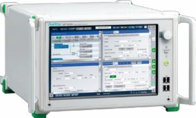 Signal Quality Analyzer-R MP1900A
 Network Master Pro MT1040A
The post Photonics-electronics Convergence Technology Becomes Essential to Next-generation DCs Precise Measurements Required for DCI Evaluation appeared first on ELE Times.
Driving the Future of Vehicle E/E Architecture: Arrow Electronics to Support Next-Generation Mobility
By
- Murdoch Fitzgerald, chief growth officer of global services for Arrow’s global components business, and
- Dr. Raphael Salmi, president of Arrow Electronics’ South Asia, Korea & Japan components business
The automotive industry is rapidly advancing toward architectures built for high‑bandwidth data movement, centralized compute, and lifecycle‑ready software operations. Traditional distributed ECU topologies—characterized by increasing wiring mass, point‑to‑point signaling, and proliferation of function-specific modules—are no longer adequate to meet the computational and functional demands of modern vehicles. E/E architecture is vital to this transformation because it provides the foundational electrical, networking, and computing framework required to support higher data throughput, real‑time decision‑making, and the integration of increasingly complex vehicle functions.
The global Vehicle E/E Architecture market was valued at $46.2 Bn in 2024 and is projected to reach $115.6 Bn by 2033, growing at a CAGR of 10.7% (source: Global Market Insights)
Technical Challenges and Complexities Involved in the Adoption of E/E Architecture
- Complex Interdependencies: ADAS, infotainment, and V2X must interoperate across protocols, bridging legacy and new systems.
- Cybersecurity: Increased connectivity expands the attack surface and increases security design complexity.
- Power & Thermal Management: Diverse power demands require real‑time energy and thermal control to prevent failures.
- Validation & Testing: Complex system interactions demand extensive simulation and HIL testing.
- Regulatory Compliance: E/E architectures must meet safety, emissions, and data‑privacy regulations end‑to‑end.
- Environmental Considerations: Sustainable design prioritizes recyclability and lower environmental impact.
Architectural Transformation: From Distributed ECUs to Centralized, Zonal Topologies
Next‑generation E/E architectures shift to a centralized, hierarchical model:
- High‑Performance Compute (HPC) Nodes: Centralized compute consolidates functions from multiple ECUs, reducing module count and enabling ADAS, autonomy, connectivity, and advanced diagnostics.
- Zonal Controllers: Controllers aggregate sensors and actuators by physical zone, cutting wiring length by 30–50% and harness weight by 15–30%.
- Smart Endpoints (SEPs): Ethernet‑centric networks simplify edge connectivity, replacing multiple legacy buses with scalable, deterministic communications.
- High‑Speed Interconnect & Power Distribution: Advanced connectors, harnesses, Ethernet, timing, and power components ensure signal integrity, EMC stability, and high‑speed performance.
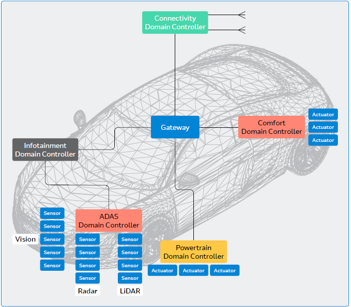
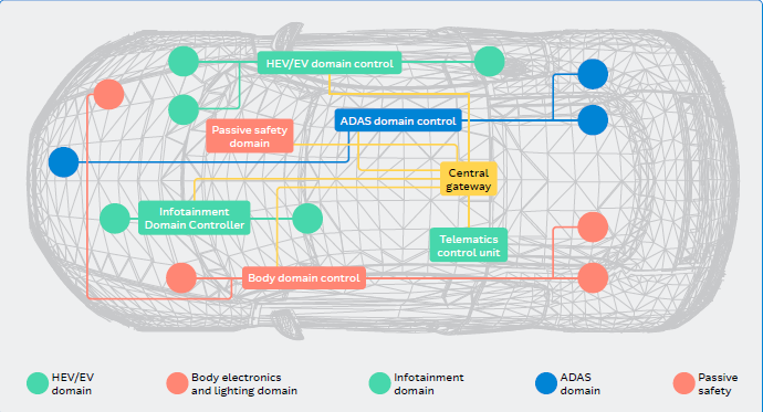
E/E Architecture: Engineering the New Vehicle Nervous System
To support this transformation, Arrow Electronics has launched a strategic initiative and dedicated research hub focused on enabling robust next‑generation Electrical and Electronic (E/E) architectures. The initiative addresses critical design, integration, and supply‑chain requirements for OEM and tier‑1 engineering teams building the next wave of mobility platforms.
Arrow Electronics: Technical Enablement Across the Full E/E Stack
Cross Disciplinary Engineering Support: Arrow’s initiative provides engineering teams with access to expertise spanning semiconductors, networking, IP&E, system architecture, safety, and cybersecurity. This includes:
- Architecture level guidance on HPC, zonal, and endpoint implementation
- Safety and cybersecurity engineering aligned to ISO 26262, ISO 21434, and UN R155 expectations
- Power distribution and 48V readiness design considerations
- EMC-driven component selection for high-speed Ethernet and mixed signal environments
This interdisciplinary support helps design teams reduce risk early in platform development.
“E/E architecture is the cornerstone of the modern automotive revolution, enabling the transition from hardware-centric machines to intelligent, software-defined mobility,” said Murdoch Fitzgerald, chief growth officer of global services for Arrow’s global components business. “By combining our global engineering reach with a broad range of components and specialized software expertise, we are well positioned to help our customers navigate this complexity, reducing their time-to-market and helping ensure their platforms are built to adapt as the industry evolves.”
Comprehensive Technology Ecosystem
Arrow’s portfolio includes components and subsystems essential to modern architectures, such as:
- Vehicle networking processors and real-time controllers
- PCIe switching and high-speed interconnect devices
- Automotive Ethernet PHYs, switches, MACsec enabled devices
- High-speed connectors and automotive-grade cabling ecosystems
- Automotive memory, storage, timing, and power components
Access to these technologies simplifies system integration and allows rapid architecture prototyping.
Strengthened Software & Safety Capabilities: Through expanded software engineering centers and the addition of established automotive software firms, Arrow now supports:
- AUTOSAR Classic and Adaptive development
- System-level modelling, HIL/SIL workflows, and model-based development
- OTA and diagnostic pipeline development
- Functional safety engineering and cybersecurity analysis
These capabilities enable engineering teams to build systems that are robust, certifiable, and scalable across vehicle lines.
Automotive Grade Supply Chain Reliability: Modern vehicle platforms require stable, long lifecycle, traceable electronic components. Arrow supports engineers with:
- Multi-sourced, risk-balanced component strategies
- Lifecycle and obsolescence planning
- Global inventory breadth across semiconductor and IP&E categories
This mitigates supply chain risk during development, validation, and production scaling.
Arrow’s E/E Architecture Research Hub
To accelerate architecture development, Arrow has launched an external research hub providing:
- Technical whitepapers
- High-level and subsystem-specific design guidance
- Deep dive analyses of HPC, zonal, and endpoint architectures
- Reference material on safety, cybersecurity, and diagnostics
- Component selection insights and technology mappings
The hub is designed as a resource for engineers, architects, and procurement specialists engaged in next-generation platform design.
 E/E architecture represents a complete overhaul of the “nervous system” within modern vehicles. Photo copyright 2026 Artlist Ltd.
 Arrow Electronics is a central solution aggregator for E/E architecture, bridging the gap between individual components and complete, integrated systems.
Photo copyright 2026 Artlist Ltd.
Local customer success case:
Arrow Electronics Fuels SAVART Motors’ EV Manufacturing Expansion in Indonesia, Boosting engineering and supply chain capabilities to drive sustainable e-mobility
Arrow has supported Indonesia’s homegrown EV maker SAVART Motors in designing and manufacturing high-quality, safe, and affordable electric scooters.
Founded in 2018, SAVART Motors stands out as one of the few local brands with in-house R&D capabilities, advanced prototyping hardware and software, and a dedicated testing and manufacturing facility in Mojokerto, East Java, Indonesia.
Indonesia’s motorcycle market is the third largest in the world. With nearly 130 million motorcycles on the road, the emissions from these vehicles significantly impact air quality and contribute to climate change. To address this, Indonesia aims to have 13 million electric two-wheelers on the roads by 20302, reducing greenhouse gas emissions and air pollution while promoting eco-friendly commuting.
Empowering homegrown EV entrepreneurs to drive electrification and e-mobility, SAVART Motors meticulously designs its electric scooters from the ground up, seamlessly integrating design aesthetics and performance to suit road conditions, riding culture, and local market expectations. With a strong commitment to quality, safety, comfort, and R&D excellence, the majority of electrical and mechanical components are developed in-house by a team of dedicated and talented engineers who are graduates of leading universities in Indonesia.
SAVART Motors is electrifying Indonesia’s transportation landscape by designing and manufacturing its electric vehicles almost entirely in-house. The company has reached a significant milestone with a 74.27% TKDN verification, reflecting the high level of domestic content in its goods and services produced in Indonesia. From concept through production, SAVART’s engineers develop cutting-edge technology tailored to the needs of local riders. Through its collaboration with Arrow Electronics, SAVART gains access to advanced components from leading global brands such as Analog Devices, Infineon, Littelfuse, Quectel, and STMicroelectronics. Arrow’s support strengthens SAVART’s designs, accelerates production timelines, and enables efficient scaling, while helping the company maintain its commitment to quality and innovation as a homegrown Indonesian brand.
“Electrification and AI-powered technologies are fundamentally transforming transportation,” said Dr. Raphael Salmi, president of Arrow Electronics’ South Asia, Korea & Japan components business. “We are excited to provide SAVART Motors with the essential engineering capabilities and supply chain services they need to manufacture EVs that not only prioritize safety, comfort, and ease of use but also cater to the needs of Indonesian riders. By offering a comprehensive technology portfolio that includes smart IoT connectivity modules, microprocessors, sensors, and automotive-grade silicon carbide MOSFETs, we are well-positioned to be their trusted technology supplier as they continue to revolutionize sustainable e-mobility in Indonesia and beyond.”
A substantial portion of the electronic components in SAVART Motors’ latest model has been sourced and supplied by Arrow. In addition to complementing SAVART Motors’ in-house R&D efforts, Arrow has provided engineering support and guidance on system integration, including adaptive user interfaces, smart vehicle control units, AI-based user profiling, keyless and fingerprint security access, and smart battery management systems.
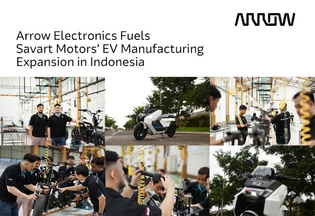
The post Driving the Future of Vehicle E/E Architecture: Arrow Electronics to Support Next-Generation Mobility appeared first on ELE Times.
Designing AI-resistant technical evaluations
Courtesy: Anthropic
What we learned from three iterations of a performance engineering take-home that Claude keeps beating.
Evaluating technical candidates becomes harder as AI capabilities improve. A take-home that distinguishes well between human skill levels today may be trivially solved by models tomorrow, rendering it useless for evaluation.
Since early 2024, our performance engineering team has used a take-home test where candidates optimise code for a simulated accelerator. Over 1,000 candidates have completed it, and dozens now work here, including engineers who brought up our Trainium cluster and shipped every model since Claude 3 Opus.
But each new Claude model has forced us to redesign the test. When given the same time limit, Claude Opus 4 outperformed most human applicants. That still allowed us to distinguish the strongest candidates—but then Claude Opus 4.5 matched even those. Humans can still outperform models when given unlimited time, but under the constraints of the take-home test, we no longer have a way to distinguish between the output of our top candidates and our most capable model.
I’ve now iterated through three versions of our take-home in an attempt to ensure it still carries a signal. Each time, I’ve learned something new about what makes evaluations robust to AI assistance and what doesn’t.
This post describes the original take-home design, how each Claude model defeated it, and the increasingly unusual approaches I’ve had to take to ensure our test stays ahead of our top model’s capabilities. While the work we do has evolved alongside our models, we still need stronger engineers—just increasingly creative ways to find them.
To that end, we’re releasing the original take-home as an open challenge, since with unlimited time, the best human performance still exceeds what Claude can achieve. If you can best Opus 4.5, we’d love to hear from you—details are at the bottom of this post.
The origin of the take-home
In November 2023, we were preparing to train and launch Claude Opus 3. We’d secured new TPU and GPU clusters, our large Trainium cluster was coming, and we were spending considerably more than we had in the past on accelerators, but we didn’t have enough performance engineers for our new scale. I posted on Twitter asking people to email us, which brought in more promising candidates than we could evaluate through our standard interview pipeline, a process that consumes significant time for staff and candidates
We needed a way to evaluate candidates more efficiently. So, I took two weeks to design a take-home test that could adequately capture the demands of the role and identify the most capable applicants.
Design goals
Take-homes have a bad reputation. Usually, they’re filled with generic problems that engineers find boring and which make for poor filters. My goal was different: create something genuinely engaging that would make candidates excited to participate and allow us to capture their technical skills at a high-level of resolution.
The format also offers advantages over live interviews for evaluating performance engineering skills:
- Longer time horizon: Engineers rarely face deadlines of less than an hour when coding. A 4-hour window (later reduced to 2 hours) better reflects the actual nature of the job. It’s still shorter than most real tasks, but we need to balance that with how onerous it is.
- Realistic environment: No one is watching or expecting narration. Candidates work in their own editor without distraction.
- Time for comprehension and tooling: Performance optimisation requires understanding existing systems and sometimes building debugging tools. Both are hard to realistically evaluate in a normal 50-minute interview.
- Compatibility with AI assistance: Anthropic’s general candidate guidance asks candidates to complete take-homes without AI unless indicated otherwise. For this take-home, we explicitly indicate otherwise.
Longer-horizon problems are harder for AI to solve completely, so candidates can use AI tools (as they would on the job) while still needing to demonstrate their own skills.
Beyond these format-specific goals, I applied the same principles I use when designing any interview to make the take-home:
- Representative of real work: The problem should give candidates a taste of what the job actually involves.
- High signal: The take-home should avoid problems that hinge on a single insight and ensure candidates have many chances to show their full abilities — leaving as little as possible to chance. It should also have a wide scoring distribution and ensure enough depth that even strong candidates don’t finish everything.
- No specific domain knowledge: People with good fundamentals can learn specifics on the job. Requiring narrow expertise unnecessarily limits the candidate pool.
- Fun: Fast development loops, interesting problems with depth, and room for creativity.
The simulated machine
I built a Python simulator for a fake accelerator with characteristics that resemble TPUs. Candidates optimise code running on this machine, using a hot-reloading Perfetto trace that shows every instruction, similar to the tooling we have on Trainium.
The machine includes features that make accelerator optimisation interesting: manually managed scratchpad memory (unlike CPUs, accelerators often require explicit memory management), VLIW (multiple execution units running in parallel each cycle, requiring efficient instruction packing), SIMD (vector operations on many elements per instruction), and multicore (distributing work across cores).

The task is a parallel tree traversal, deliberately not deep learning flavoured, since most performance engineers hadn’t worked on deep learning yet and could learn domain specifics on the job. The problem was inspired by branchless SIMD decision tree inference, a classical ML optimisation challenge as a nod to the past, which only a few candidates had encountered before.
Candidates start with a fully serial implementation and progressively exploit the machine’s parallelism. The warmup is multicore parallelism, then candidates choose whether to tackle SIMD vectorisation or VLIW instruction packing. The original version also included a bug that candidates needed to debug first, exercising their ability to build tooling.
Early results
The initial take-home worked well. One person from the Twitter batch scored substantially higher than everyone else. He started in early February, two weeks after our first hires through the standard pipeline. The test proved predictive: He immediately began optimising kernels and found a workaround for a launch-blocking compiler bug involving tensor indexing math overflowing 32 bits.
Over the next year and a half, about 1,000 candidates completed the take-home, and it helped us hire most of our current performance engineering team. It proved especially valuable for candidates with limited experience on paper: several of our highest-performing engineers came directly from undergrad but showed enough skill on the take-home for us to hire confidently.
Feedback was positive. Many candidates worked past the 4-hour limit because they were enjoying themselves. The strongest unlimited-time submissions included full optimising mini-compilers and several clever optimisations I hadn’t anticipated.
Then Claude Opus 4 defeated it
By May 2025, Claude 3.7 Sonnet had already crept up to the point where over 50% of candidates would have been better off delegating to Claude Code entirely. I then tested a pre-release version of Claude Opus 4 on the take-home. It came up with a more optimised solution than almost all humans did within the 4-hour limit.
This wasn’t my first interview defeated by a Claude model. I’d designed a live interview question in 2023 specifically because our questions at the time were based around common tasks that early Claude models had lots of knowledge of and so could solve easily. I tried to design a question that required more problem-solving skill than knowledge, still based on a real (but niche) problem I’d solved at work. Claude 3 Opus beat part 1 of that question; Claude 3.5 Sonnet beat part 2. We still use it because our other live questions aren’t AI-resistant either.
For the take-home, there was a straightforward fix. The problem had far more depth than anyone could explore in 4 hours, so I used Claude Opus 4 to identify where it started struggling. That became the new starting point for version 2. I wrote cleaner starter code, added new machine features for more depth, and removed multicore (which Claude had already solved, and which only slowed down development loops without adding signal).
I also shortened the time limit from 4 hours to 2 hours. I’d originally chosen 4 hours based on candidate feedback, preferring less risk of getting sunk if they got stuck for a bit on a bug or confusion, but the scheduling overhead was causing multi-week delays in our pipeline. Two hours is much easier to fit into a weekend.
Version 2 emphasised clever optimisation insights over debugging and code volume. It served us well for several months.
Then Claude Opus 4.5 defeated that
When I tested a pre-release Claude Opus 4.5 checkpoint, I watched Claude Code work on the problem for 2 hours, gradually improving its solution. It solved the initial bottlenecks, implemented all the common micro-optimisations, and met our passing threshold in under an hour.
Then it stopped, convinced it had hit an insurmountable memory bandwidth bottleneck. Most humans reach the same conclusion. But there are clever tricks that exploit the problem structure to work around that bottleneck. When I told Claude the cycle count it was possible to achieve, it thought for a while and found the trick. It was then debugged, tuned, and implemented with further optimisations. By the 2-hour mark, its score matched the best human performance within that time limit—and that human had made heavy use of Claude 4 with steering.
We tried it out in our internal test-time compute harness for more rigour and confirmed it could both beat humans in 2 hours and continue climbing with time. Post-launch, we even generically improved our harness and got a higher score.

I had a problem. We were about to release a model where the best strategy on our take-home would be delegating to Claude Code.
Considering the options
Some colleagues suggested banning AI assistance. I didn’t want to do this. Beyond the enforcement challenges, I had a sense that given people continue to play a vital role in our work, I should be able to figure out some way for them to distinguish themselves in a setting with AI, as they’d have on the job. I didn’t want to give in yet to the idea that humans only have an advantage on tasks longer than a few hours.
Others suggested raising the bar to “substantially outperform what Claude Code achieves alone.” The concern here was that Claude works fast. Humans typically spend half the 2 hours reading and understanding the problem before they start optimising. A human trying to steer Claude would likely be constantly behind, understanding what Claude did only after the fact. The dominant strategy might become sitting back and watching.
Nowadays, performance engineers at Anthropic still have lots of work to do, but it looks more like tough debugging, systems design, performance analysis, figuring out how to verify the correctness of our systems, and figuring out how to make Claude’s code simpler and more elegant. Unfortunately, these things are tough to test in an objective way without a lot of time or common context. It’s always been hard to design interviews that represent the job, but now it’s harder than ever.
But I also worried if I invested in designing a new take-home, either Claude Opus 4.5 would solve that too, or it would become so challenging that it would be impossible for humans to complete in two hours.
Attempt 1: A different optimisation problem
I realised Claude could help me implement whatever I designed quickly, which motivated me to try developing a harder take-home. I chose a problem based on one of the trickier kernel optimisations I’d done at Anthropic: an efficient data transposition on 2D TPU registers while avoiding bank conflicts. I distilled it into a simpler problem on a simulated machine and had Claude implement the changes in under a day.
Claude Opus 4.5 found a great optimisation I hadn’t even thought of. Through careful analysis, it realised it could transpose the entire computation rather than figuring out how to transpose the data, and it rewrote the whole program accordingly.
In my real case, this wouldn’t have worked, so I patched the problem to remove that approach. Claude then made progress but couldn’t find the most efficient solution. It seemed like I had my new problem, now I just had to hope human candidates could get it fast enough. But I had some nagging doubt, so I double-checked using Claude Code’s “ultrathink” feature with longer thinking budgets … and it solved it. It even knew the tricks for fixing bank conflicts.
In hindsight, this wasn’t the right problem to try. Engineers across many platforms have struggled with data transposition and bank conflicts, so Claude has substantial training data to draw on. While I’d found my solution from first principles, Claude could draw on a larger toolbox of experience.
Attempt 2: Going weirder
I needed a problem where human reasoning could win over Claude’s larger experience base: something sufficiently out of distribution. Unfortunately, this conflicted with my goal of being recognizably like the job.
I thought about the most unusual optimisation problems I’d enjoyed and landed on Zachtronics games. These programming puzzle games use unusual, highly constrained instruction sets that force you to program in unconventional ways. For example, in Shenzhen I/O, programs are split across multiple communicating chips that each hold only about 10 instructions with one or two state registers. Clever optimisation often involves encoding state into the instruction pointer or branch flags.
I designed a new take-home consisting of puzzles using a tiny, heavily constrained instruction set, optimising solutions for minimal instruction count. I implemented one medium-hard puzzle and tested it on Claude Opus 4.5. It failed. I filled out more puzzles and had colleagues verify that people less steeped in the problem than I could still outperform Claude.
Unlike Zachtronics games, I intentionally provided no visualisation or debugging tools. The starter code only checks whether solutions are valid. Building debugging tools is part of what’s being tested: you can either insert well-crafted print statements or ask a coding model to generate an interactive debugger in a few minutes. Judgment about how to invest in tooling is part of the signal.
I’m reasonably happy with the new take-home. It might have lower variance than the original because it comprises more independent sub-problems. Early results are promising: scores correlate well with the calibre of candidates’ past work, and one of my most capable colleagues scored higher than any candidate so far.
I’m still sad to have given up the realism and varied depth of the original. But realism may be a luxury we no longer have. The original worked because it resembled real work. The replacement works because it simulates novel work.
The post Designing AI-resistant technical evaluations appeared first on ELE Times.
Why Connected MCUs Are Replacing Bolt-On Wireless in IoT Devices?
Courtesy: Infineon
Connected MCUs are gaining popularity rapidly.
If you’ve spent any time building or supporting connected products over the last decade, you’ve seen the pattern repeat itself: a product team realises they need wireless, so they bolt on a Wi-Fi module, wire up SDIO or SPI, route antennas where there’s some available space, and duct-tape the firmware stack into place right before release.
It works…until it doesn’t. And the truth is, most of us knew it was going to be painful the moment that architecture was chosen.
Whether it’s a forklift, a vitals monitoring device, a handheld scanner, or an HVAC controller, the problems are surprisingly universal. And they all stem from the same root issue.
Wireless was treated like an accessory instead of a part of the system.
We’re finally at a turning point. Connected MCUs, especially with integrated Wi-Fi 6 and 6E, change the entire equation.
Let me walk you through why this shift is happening and what it solves.
The pain: Bolt-on wireless was never as simple as it looked
Customers usually come with the same set of problems:
- Integration complexity snowballs quickly
That “easy” SDIO Wi-Fi module seems fine at first, until you realise:
- Your host processor can’t keep up under load
- The driver needs specific kernel patches
- The layout constraints choke your antenna performance
- You’re juggling two separate firmware roadmaps
By the end, half the schedule is spent debugging issues no one originally accounted for.
- RF performance suffers because it has to fit the enclosure, not the system
Bolt-on designs force antennas into whatever space is left. That might be inside a forklift mast, behind a metal enclosure, or buried under plastic in a medical device.
You can predict the RF problems before they happen, and yet they still happen.
- Certifications slow everything down
When wireless is a separate module, you:
- Test the radio module for compliance
- Test your host MCU for EMI
- You have to do integration testing when you put them together
- And then redo it every time you want to change the antenna
Teams underestimate this every single time.
- The BOM cost keeps going higher
One board for the host MCU, one for wireless, external memory, custom harnesses, enclosures… By the time the full system is built, the wireless subsystems cost more than the product owner ever expected.
And in long-lifecycle industries, like material handling, medical, and commercial HVAC, that pain compounds across entire product lines.
The turning point: Wi-Fi 6 and 6E connected MCUs
The reason this shift is happening is simple:
We finally have connected MCUs that are powerful enough, low-power enough, and secure enough to replace external wireless subsystems entirely.
This means the wireless subsystem is no longer bolted on. It’s a self-contained compute & connectivity module that slides directly into your main system design. For the first time, the architecture reflects how engineers actually want to build products:
A single module that handles wireless, networking, security, protocol stacks, and memory, rather than scattering those components across multiple boards.
Simplifying the integration, RF performance, and certification challenges that discrete systems have.
The post Why Connected MCUs Are Replacing Bolt-On Wireless in IoT Devices? appeared first on ELE Times.
R&S’s next-generation Wi-Fi 8 access point testing in collaboration with NETGEAR
NETGEAR has selected the CMP180 radio communication tester from Rohde & Schwarz for the development of future Wi-Fi 8 access points. By integrating the tester into their design validation test environment, NETGEAR will be able to speed up the development of performance-optimised Wi-Fi products.
Rohde & Schwarz, a leading supplier of test and measurement equipment for wireless applications, and NETGEAR, manufacturer of advanced networking technologies and leading-edge Wi-Fi 7 products, collaborate to get the next generation Wi-Fi 8 products ready for the market.
Wi-Fi 8 is the next generation Wi-Fi based on the upcoming IEEE 802.11bn standard. With the focus on ultra-high reliable (UHR) WLAN, this new technology will improve the wireless user experience at homes, offices and factories: high-speed connectivity under all conditions with low latency for gaming, learning and working applications, which will use augmented reality (AR) and virtual reality (VR) to provide an immersive user experience.
Design validation of Wi-Fi 8 access points requires test solutions which support the latest Wi-Fi 8 features like distributed resource units (DRU) or unequal modulation (UEQM) with up to 320 MHz wide channels in all supported bands and highest modulation schemes (4096QAM), while providing the performance (EVM), and scalability (4×4 MIMO) required to optimize the wireless device performance.
Rohde & Schwarz provides NETGEAR with the CMP180 radio communication tester, a future-proof non-signalling testing solution for wireless devices, which can be used in research, development, validation and production. It supports many cellular and non-cellular technologies, including the latest Wi-Fi 6E, Wi-Fi 7, Wi-Fi 8 and 5G NR FR1 in frequencies up to 8 GHz and bandwidths of up to 500 MHz.
The CMP180 comes equipped with two analysers, two generators and two times eight RF ports in a single box, plus the possibility to scale up by stacking several testers. This makes it a cost-efficient test solution with best-in-class performance, addressing current and future test demands.
While its fast multi-DUT testing capabilities make the CMP180 ideal for testing in mass-production test environments, test engineers can use the instrument throughout the entire development cycle: from engineering validation tests (EVT), design validation tests (DVT) and production validation tests (PVT) to mass production (MP).
Joseph Emmanuel, VP, Consumer Business Unit HW Engineering at NETGEAR, says: “Working with Rohde & Schwarz enables us to bring our Wi-Fi 8 products on the market with the expected high quality and extremely high performance for the best multi-gigabit Wi-Fi experience everywhere at home.”
Goce Talaganov, Vice President Mobile Radio Testers at Rohde & Schwarz, says: “We are grateful for the close collaboration with NETGEAR on the latest Wi-Fi 8 technology. Our experience in wireless device testing and early cooperation with Wi-Fi 8 chipset and device vendors helped us to improve our test solution for the upcoming broad Wi-Fi 8 market.”
The post R&S’s next-generation Wi-Fi 8 access point testing in collaboration with NETGEAR appeared first on ELE Times.
Redefining Precision: How CNC Robotics is Transforming Machining with SINUMERIK Machine Tool Robot
Courtesy: Siemens
Walk into any modern factory, and you’ll meet robots: palletising, tending, loading, unloading. Useful? Absolutely. But using them for more advanced robotic tasks like machining steel with tight tolerances, you’ll always hear the old refrain: “Robots aren’t rigid enough,” like in textbooks and lectures. That was then. Today, CNC robots shorten the distance between the agility of industrial robots and the precision of machine tools. And at the centre of that shift is the SINUMERIK Machine Tool Robot (MTR) – the first robot we can confidently call a machining asset, with steel milling capabilities and more, not just an automation helper.
In this article, you can find the following three things:
- Learn what “CNC robotics” means and what robots do on the shopfloor today.
- Understand why the SINUMERIK Machine Tool Robot is different.
- Zoom out to CNC Robotics as a whole and the practical benefits you can expect.
Along the way, we will challenge a couple of comfortable assumptions in the industry. Consider it as an invitation to rethink what a robot can be used for and also where it unleashes new automation potential.
CNC Robotics: From “Good at Handling” to “Great at Machining”
For years, robots excelled at tasks with low process forces, such as handling, assembly, welding, or laser cutting. They’re flexible, they have reach, and they integrate well around machines. But whenever we crossed the line into machining, conventional robot mechanics and their controls hit a wall: Insufficient stiffness and path accuracy under load, slow machining, and vibrations. That reality entrenched a mindset: “Let machines machine, let robots move things.”
SINUMERIK CNC robotics aims to break that model by putting CNC-grade motion control and digital workflows into the robot’s core. With SINUMERIK, that means:
- A control concept that treats the robot like a machine tool, not a black‑box auxiliary.
- Integration into the SINUMERIK ONE CNC environment (including a digital twin for simulation and validation before the first cut).
- A solution family that spans from simple connections for handling through to full high‑precision motion control of machines using robot kinematics, meeting you where you are on the automation journey.
“If robots still strike you as unsuitable for high‑precision tasks, the latest developments may surprise you.”
Meet the SINUMERIK Machine Tool Robot: a Robot That Machines Like a Machine
At the core of the story is this: Siemens developed the SINUMERIK Machine Tool Robot (MTR) technology, combining the agility of a 6‑axis robot with the precision of a CNC machine tool. So how did we achieve that?
- Machine‑tool‑grade control: The MTR is controlled by SINUMERIK ONE, Siemens’ digital‑native CNC. It lets a robot inherit machine‑tool behaviours for high-precision path tasks.
- Measured gains: Compared to conventional industrial robots, users can expect over 200% higher path accuracy and significantly higher dynamic stiffness. That’s the difference between “good enough for trimming” and “great even for steel.”
- Real productivity: The new control concept delivers 20–40% productivity increases, which is also compelling in non‑process-force path processes (laser, waterjet) where speed and path smoothness dominate.
Now, let’s add something from the shopfloor perspective, we don’t say enough: the user experience is as critical as the physics of the process. With SINUMERIK ONE, the digital twin lets you verify programs, validate reach and sequence, and fine-tune before you ever stop the line, all with existing machine tool programming know-how. Commissioning becomes a digital problem first, a hardware problem second – and that’s a non-trivial cultural shift.
Recognition Matters: Innovators of the Year
Breakthroughs like this don’t exist in a vacuum. The hybrid‑drive system, developed together with Fraunhofer Institute for Manufacturing Technology and Advanced Materials and Siemens colleagues, was recognised with the Siemens “Inventor of the Year” award.
“Swiss Army Knife” Machining – Brought to Life by Hybrid Drive Innovation
A core complaint against machining with robots has been stiffness under process forces, especially in heavy-duty machining of steel or tough alloys. Here’s where an innovative hybrid drive concept changes the picture.
- By combining the strengths of direct motors (precision, speed) and geared motors (robustness, power), the hybrid approach delivers both sensitivity and muscle.
- Robots equipped this way stay stable and have low vibration at high feed rates, even under strong process‑force excitation, approaching the precision and dynamics of classic machine tools.
- The result is a robot that genuinely evolves into the “Swiss Army knife” of manufacturing: precision machining where needed, agile flexibility everywhere else, with a smaller overall footprint.
This isn’t just a technical refinement; it affects practical operations: it can reduce floor‑space requirements and lower energy use per part.
The post Redefining Precision: How CNC Robotics is Transforming Machining with SINUMERIK Machine Tool Robot appeared first on ELE Times.
Сторінки

