
ELE Times

DigiKey Expands Asian Electronics Industry with Launch of Vietnam Website
DigiKey, the global distributor of electronic components and automation products, announces the launch of its regional Vietnam website. The new website is tailored to meet the escalating demand for robust supply chain solutions in Vietnam’s expanding electronics and manufacturing sectors.
Vietnam’s exports of computers, electronic products, and components reached $30.72 billion in Q1 of 2026, a 45.5% year-on-year increase, according to Vietnam Customs, underscoring the industry’s role as a leading driver of export growth. Vietnam also remained one of the world’s top mobile phone exporters, ranking third globally, making it an ideal market for DigiKey to support as it grows as a key hub for global electronics manufacturing and supply chain diversification.
“The new DigiKey Vietnam website demonstrates our commitment to supporting our partners and customers in one of Asia’s most dynamic markets,” said Dave Doherty, CEO for DigiKey. “This new platform gives Vietnamese customers access to DigiKey’s global inventory of more than 18 million products, with an emphasis on tailored, localized support and faster, frictionless digital tools. We are thrilled to empower Vietnam’s electronics industry with improved supply chain visibility and custom solutions.”
The post DigiKey Expands Asian Electronics Industry with Launch of Vietnam Website appeared first on ELE Times.
India’s Defence Boom Risks 10 Years Order Backlog: PwC Study
India’s aerospace and defence (A&D) sector is entering a high-growth phase. Still, execution constraints emerge as the biggest risk to sustaining momentum, according to a new PwC India study titled ‘Accelerating aerospace and defence manufacturing through operational excellence and supply chain resilience’.
The A&D sector is ready to play a catalytic role in India’s economic transformation, helping drive the nearly 16-fold expansion in manufacturing needed to realise the country’s ambition of a $30 trillion economy by 2047. While strong demand, rising exports, and policy support have firmly positioned A&D manufacturing as a key pillar of India’s economic growth, the study highlights that large order backlogs—potentially taking up to a decade to clear—could test the sector’s ability to deliver at scale.
“For India’s aerospace and defence sector, the next phase of growth will be shaped not just by demand, but by the ability to execute with consistency, speed, and precision with scale. Companies that strengthen planning, modernise operations, and build resilient, digitally connected supply chains will be best placed to convert today’s order pipeline into timely, high-quality output at scale,” says Captain Vishal Kanwar, Aerospace Defence and Space Leader, PwC India.
Execution is the real challenge, not the demand
India’s A&D sector is at a turning point. Demand is strong. Exports are rising. But the next phase will be defined by one thing: execution at scale. India now exports defence products to nearly 100 countries. Domestic defence production reached a record ₹1.54 lakh crore in FY25. Yet, large order books are creating pressure on delivery capacity.
For major manufacturers, order backlogs are already significant:
- 1.71x to 6.88x order book-to-revenue multiples
- 2–7 years of execution backlog
- In some segments, up to 5–10 years to clear existing orders
This points to a clear structural challenge. As Dinesh Arora, Partner and Leader, Advisory, PwC India, notes: “The real test for India’s aerospace and defence sector is no longer whether demand exists, but whether the ecosystem can execute with speed, precision, and resilience. As order books expand, companies will need to move beyond incremental capacity addition and fundamentally strengthen planning, shopfloor productivity, supplier coordination, and digital integration. Those that build these capabilities early will be better positioned to convert growth momentum into reliable, globally competitive delivery. Put simply, India has the opportunity. Now it must build the execution engine to match it.”
The blueprint to convert backlog into output
To address the widening gap between order books and execution capacity, the study outlines six priority transformation areas:
- Supply chain efficiency
- Operational excellence
- Planning and governance
- R&D acceleration
- Workforce productivity
- Digital integration (digital thread)
These transformation levers will help the sector move from backlog-led growth to execution-led scale—from stronger operations and shopfloor discipline to digital integration, fostering indigenous vendor ecosystems and supply chain resilience, and smarter use of advanced technologies. These shifts collectively enhance productivity, minimise rework, and provide manufacturers with the necessary tools to execute operations faster, more reliably, and in line with global competitive standards.
The post India’s Defence Boom Risks 10 Years Order Backlog: PwC Study appeared first on ELE Times.
Implantable and Non-Invasive Continuous Health Sensors
Continuous health monitoring is transforming modern medicine. Instead of relying only on occasional hospital visits and laboratory tests, doctors and patients can now access real-time physiological data through advanced sensors. These technologies are broadly divided into two categories: implantable sensors placed inside the body and non-invasive wearable sensors used externally. Together, they are reshaping healthcare by enabling early disease detection, personalized treatment, and remote patient monitoring.
The Rise of Continuous Health Monitoring
Traditional healthcare systems often depend on periodic measurements such as blood pressure checks or glucose testing. However, many medical conditions change continuously throughout the day. Diseases like diabetes, heart disorders, hypertension, and respiratory illnesses require constant observation to prevent complications.
Continuous health sensors solve this problem by collecting data 24/7. Modern devices can monitor heart rate, blood glucose, oxygen saturation, body temperature, movement, respiration, and even biochemical markers in sweat or interstitial fluid. Advances in microelectronics, wireless communication, artificial intelligence (AI), and biosensor engineering have accelerated the development of these smart healthcare systems.
Implantable Health Sensors
Implantable sensors are devices inserted under the skin or within organs to monitor biological signals directly from the body. These sensors provide highly accurate and continuous data because they interact closely with tissues and body fluids.
Examples of Implantable Sensors
One of the most successful implantable technologies is the continuous glucose monitor (CGM) used for diabetes management. Devices such as implantable glucose sensors can remain under the skin for months and transmit blood sugar readings to smartphones in real time. Recent FDA-cleared systems can operate for up to one year before replacement.
Another major application is implantable cardiac monitors. These miniature devices continuously track heart rhythms and help physicians detect arrhythmias or irregular heartbeats. Modern systems are tiny, minimally invasive, and capable of remote data transmission to healthcare providers.
Researchers are also developing advanced implantable biosensors capable of measuring oxygen levels, tissue health, metabolic activity, and even neurological signals. Some experimental devices are battery-free and powered wirelessly through magnetic or inductive coupling technologies.
Illustration: Implantable Biosensor Technology

Implantable sensors offer several important advantages:
- High measurement accuracy due to direct contact with internal tissues
- Continuous long-term monitoring without user intervention
- Early detection of medical emergencies
- Improved disease management and personalized treatment
- Reduced hospital visits through remote monitoring
These devices are especially useful for chronic diseases that require precise data over long periods.
Challenges and RisksDespite their advantages, implantable devices face technical and ethical challenges. Biocompatibility is critical because the body may react negatively to foreign materials. Power supply and wireless communication remain engineering challenges, particularly for miniaturized implants.
Cybersecurity is another concern. Since implantable devices transmit sensitive health data wirelessly, they may become targets for hacking or unauthorized access. Researchers are therefore developing secure communication protocols for medical implants.
Non-Invasive Wearable SensorsNon-invasive sensors are external devices worn on the body. These include smartwatches, fitness bands, adhesive patches, smart clothing, and portable biosensors. Wearables have become extremely popular because they are convenient, affordable, and easy to use.
Modern wearable devices can measure heart rate, electrocardiograms (ECG), sleep patterns, stress levels, physical activity, oxygen saturation, and body temperature. Some advanced systems also estimate blood pressure and glucose levels using optical or electrochemical techniques.
Illustration: Wearable Health Monitoring DevicesWearable Biosensors in Healthcare
Wearable biosensors are increasingly used in hospitals and home healthcare environments. Chest-worn biosensors can continuously monitor ECG, respiration, temperature, and motion while transmitting data to cloud platforms for medical analysis.
Smartwatches now include AI-driven health features capable of detecting irregular heart rhythms and providing health alerts. During the COVID-19 pandemic, wearable monitoring gained importance because patients could be observed remotely without frequent hospital visits.
Flexible and epidermal sensors are another exciting innovation. These ultra-thin electronic patches attach directly to the skin and can monitor sweat composition, hydration, muscle activity, and biochemical signals with minimal discomfort.
Role of Artificial Intelligence and Big Data
Artificial intelligence is becoming a central component of continuous health monitoring systems. AI algorithms analyze sensor data to identify abnormalities, predict disease risks, and provide personalized recommendations.
For example, AI can detect early signs of atrial fibrillation from smartwatch ECG data or predict dangerous glucose fluctuations before symptoms occur. Cloud computing and Internet of Things (IoT) technologies allow healthcare providers to monitor thousands of patients remotely and respond quickly during emergencies.
The integration of AI with biosensors is expected to create predictive healthcare systems where diseases are identified before they become severe.
Future Research and Innovations
The future of health sensors lies in miniaturization, flexibility, and multi-parameter monitoring. Researchers are developing implantable biosensors that can simultaneously measure multiple biochemical markers using advanced nanotechnology and microelectromechanical systems (MEMS).
Future devices may include:
- Battery-free implantable sensors
- Smart tattoos for biochemical monitoring
- Flexible electronic skin
- AI-powered diagnostic wearables
- Wireless neural implants
- Real-time personalized drug delivery systems
As technology advances, healthcare may shift from reactive treatment to proactive prevention.
Conclusion
Implantable and non-invasive continuous health sensors represent one of the most important technological revolutions in modern medicine. Implantable devices provide accurate internal monitoring, while wearable sensors offer convenient and affordable health tracking for everyday use. Together with AI, wireless communication, and biosensor research, these technologies are enabling a future of personalized, preventive, and data-driven healthcare.
Although challenges related to safety, cybersecurity, cost, and regulatory approval remain, continuous health sensors are expected to play a major role in improving global healthcare systems and patient quality of life in the coming decades.
The post Implantable and Non-Invasive Continuous Health Sensors appeared first on ELE Times.
The Chips That Change The World
Courtesy Texas Instruments
Why do general-purpose chips lay the foundation for technological innovations that are redefining our lives?
Do you remember when your phone was tethered to a wall? Or when a visit to the doctor was the primary way to see your health data?

Today, your phone fits in your pocket and lets you connect with anyone from almost anywhere. Wearable rings and watches offer you insight into data about your health almost instantly.
Anyone can relate to technology becoming more complex while interactions feel more effortless. Homes are becoming more responsive and automated. And intelligent vehicles are reshaping what people expect from the road. The list goes on.
Technology has silently rewritten everyday life in several ways – but how?
It starts with semiconductors.
How semiconductors enable innovation
The technology people notice first is usually the experience: the phone that lasts longer, the wearable that tracks health in real time, or the vehicle that responds intelligently.
Semiconductors are the driving force behind these electronics. Some chips, called application-specific products, are highly specialized and can integrate different functions. Others are general-purpose chips: the foundational, ubiquitous, flexible components that sometimes make up close to 90% of the ICs in an electronic system.
The two work together to help engineers optimize designs based on cost, size, availability, performance, and functionality. While general-purpose chips may not always be the most visible part of innovation, they often make innovation practical.
General-purpose chips help electronic systems sense, control, and manage power reliably. For example, engineers might use:
- Amplifiers’ signals that are converted by basic data converters and processed by microcontrollers in a smoke detector’s sensor. Clocks also provide basic timing on the board. These parts all enable the sensor to detect smoke and trigger an alarm to keep people and their belongings safe.
- Microcontrollers to manage the timing, logic, and inputs in a washing machine, helping turn a set of mechanical steps into an automatic cleaning cycle.
- Power management chips step voltages up or down inside a phone, helping each subsystem, such as the camera or display, regulate its voltage.

Why general-purpose chips are crucial
Breakthrough technology doesn’t usually start with a blank sheet of paper. It starts with a dependable foundation.
By handling essential functions such as power management, signal processing, sensing, and control, general-purpose chips free engineers to focus on what makes a design more advanced, efficient, or differentiated. Without those foundational components, development can slow, complexity can grow, and innovation can become harder to scale.
What does this look like in real life?
Imagine a data center. Have you ever thought about the millions of chips making the delivery of information feel seamless whenever you ask a large language model a question?
Inside an AI server rack, application-specific products such as AI accelerators may handle the intense parallel computations required for training and inference. But data centers also depend on a broad set of general-purpose chips, such as power management devices that control multi-stage voltage regulation, sequencing, monitoring, and protection.
Together, general-purpose and application-specific products help engineers build systems that can process massive amounts of data while balancing cost, size, power, availability, and performance at scale.
Making the power of general-purpose a reality
For engineers, the value of a general-purpose chip extends beyond the function it performs. A component used in a data center server or phone must also be available, consistent across product generations, and flexible enough to support the surrounding application-specific products.
Consider a company building several generations of connected appliances. The most visible features may change with time, but many of the foundational needs remain: managing power, reading signals, coordinating inputs, and helping the system operate reliably. When engineers can rely on a consistent set of general-purpose components across those designs, they can reduce redesign work and spend more time advancing the features customers notice.
That’s where breadth and longevity of portfolio, attentiveness to quality, manufacturing scale, and long-term consistency matter. TI’s expansive general-purpose portfolio gives designers access to widely used embedded, signal chain, and embedded parts that can support many applications, and engineers still have the flexibility to customize their selections for their needs. This breadth, combined with our continued investment in process technology, helps improve efficiency, performance, and high-quality supply over time.
Those advances can simplify development, helping engineers spend less time reworking foundational functions and more time creating electronics that are easier to scale, bring to market, and improve across product generations.
The unseen truth behind visible progress
Modern life can make extraordinary technology feel routine. Video calls across continents. Homes that sense, respond and adapt. A new generation of more sustainable and autonomous mobility. These experiences can feel seamless now, almost inevitable. But they had to start somewhere. They only exist because layers of engineering are working together with remarkable precision behind the scenes.
This is the hidden truth inside visible progress: innovation only moves forward when the fundamentals are resolved. Without general-purpose chips, development slows, complexity grows and the future takes longer to arrive.
Semiconductors don’t change the world on their own – but the world doesn’t change without them.
The post The Chips That Change The World appeared first on ELE Times.
The New Electronics World Order: Opportunity, Risk, and India’s Moment
The global electronics industry is witnessing its most significant restructuring since the rise of Asia as the world’s manufacturing hub three decades ago. What was once driven primarily by cost efficiencies and globalization is now being reshaped by geopolitics, strategic autonomy, supply chain security, and technological sovereignty. Electronics has ceased to be merely an industrial sector; it has become a geopolitical instrument.
The emergence of the “China Plus One” strategy symbolizes this transformation. Nations and corporations across the world are seeking to diversify manufacturing footprints beyond China, not necessarily to replace China, but to reduce excessive dependence on a single geography. The disruptions caused by the COVID-19 pandemic, semiconductor shortages, trade tensions, and evolving geopolitical rivalries exposed vulnerabilities in global supply chains that had long been ignored in pursuit of efficiency.
China’s dominance in electronics manufacturing remains unparalleled. From consumer electronics and telecom equipment to batteries, solar cells, and semiconductor packaging, China has built an industrial ecosystem that is difficult to replicate overnight. More importantly, it controls a substantial portion of the global rare earth value chain, including mining, refining, and processing. Rare earth elements are indispensable for electric vehicles, renewable energy systems, advanced electronics, defence platforms, and semiconductor manufacturing.

This concentration of strategic resources has become a major concern for governments worldwide. As geopolitical competition intensifies, access to critical minerals is increasingly viewed through the lens of national security. The world has learned that dependence on a single source for critical inputs can become a strategic vulnerability.
Consequently, efforts are accelerating to identify alternatives. Countries including the United States, Australia, Canada, Japan, and members of the European Union are investing heavily in alternative rare earth supply chains. Research institutions and technology companies are exploring substitute materials, recycling technologies, and rare-earth-free magnet designs. Innovations in ferrite magnets, advanced composites, nanomaterials, and material science are gradually reducing dependence on traditional rare earths in selected applications.
However, the reality remains that there is no immediate substitute for many critical rare earth elements. The challenge is not merely discovering alternatives but achieving commercial viability at scale. The future is therefore likely to be defined by a combination of diversification, recycling, strategic stockpiling, and technological innovation.
At the same time, the United States faces a different challenge. Despite being the world’s leader in semiconductor design, software, and innovation, it has struggled to maintain large-scale manufacturing competitiveness. Decades of offshoring have hollowed out portions of the manufacturing ecosystem. While initiatives such as the CHIPS Act represent a major commitment toward rebuilding domestic semiconductor capacity, establishing fabrication facilities is only one piece of the puzzle. Manufacturing excellence requires an entire ecosystem of suppliers, materials, a skilled workforce, logistics, packaging, testing, and supporting industries.
This reality underscores a fundamental lesson: manufacturing ecosystems cannot be created overnight. They evolve through sustained investments, policy consistency, talent development, and industrial clustering over decades.
Against this backdrop, India finds itself at a historic inflection point.
India’s Electronics System Design and Manufacturing (ESDM) journey has evolved remarkably over the past decade. From being largely an importer of electronic products, the country has steadily built capabilities in mobile phone manufacturing, electronics assembly, semiconductor packaging, design services, and component production. Policy initiatives such as Production Linked Incentive (PLI) schemes, semiconductor missions, design-linked incentives, and infrastructure development have begun to attract global investments.
India’s strengths extend beyond cost competitiveness. The country possesses one of the world’s largest engineering talent pools, a rapidly growing domestic market, a vibrant startup ecosystem, and increasing geopolitical trust among major global powers. As companies seek resilient and diversified supply chains, India is emerging as a credible long-term partner.
Yet, India must recognize that the opportunity presented by China Plus One is not automatic. Competing nations such as Vietnam, Thailand, Malaysia, Indonesia, and Mexico are equally determined to attract global investments. The race is not merely for assembly operations but for ownership of high-value segments including semiconductor fabrication, advanced packaging, component manufacturing, industrial electronics, defence electronics, and next-generation technologies.
The next phase of India’s ESDM evolution must therefore focus on deep manufacturing capabilities. Component ecosystems, semiconductor materials, specialty chemicals, electronic-grade gases, passive components, sensors, power electronics, and advanced manufacturing equipment need equal attention. Without these foundational layers, value addition remains limited.
The electronics industry today sits at the intersection of economics, technology, and geopolitics. Semiconductors have become strategic assets. Rare earth minerals have become instruments of influence. Supply chains have become matters of national security. Manufacturing capacity has become a measure of strategic resilience.
A new world order is emerging where technological capability will increasingly determine economic power and geopolitical influence. Nations that control critical technologies, advanced manufacturing, intellectual property, and strategic resources will shape the contours of the twenty-first century.
For India, this moment represents more than an industrial opportunity. It is an opportunity to redefine its position in the global technology landscape. The objective should not merely be to become an alternative manufacturing destination but to emerge as a technology creator, innovation hub, and trusted global electronics powerhouse.
The global electronics industry is entering an era where resilience may become as important as efficiency, strategic autonomy as important as globalization, and innovation as important as scale. In this evolving landscape, India has the potential to become one of the defining success stories of the next industrial age.
The question is no longer whether the global electronics supply chain will diversify. The question is who will lead the next chapter of that transformation.
India has a rare opportunity to ensure that it is among the leaders writing that story.
The post The New Electronics World Order: Opportunity, Risk, and India’s Moment appeared first on ELE Times.
Quantum Computing and Quantum Cryptography: The Future Beyond Binary Electronics
Introduction
For more than half a century, digital electronics has relied on binary systems in which information is represented by bits existing as either 0 or 1. From microcontrollers to supercomputers, this binary architecture has powered modern civilization. However, the increasing demand for ultra-fast computation, secure communication, and advanced artificial intelligence is pushing conventional semiconductor technology toward its physical limitations. Quantum computing and quantum cryptography are emerging as revolutionary technologies capable of transforming the future of electronics engineering.
Unlike classical systems, quantum electronics operate using qubits (quantum bits), which exploit the principles of quantum mechanics such as superposition and entanglement. These properties allow quantum computers to solve highly complex problems in seconds that would require traditional supercomputers thousands of years to complete.
Understanding Qubits
A classical bit can exist only in one state at a time: either 0 or 1. In contrast, a qubit can exist simultaneously in multiple states due to the phenomenon known as superposition.
|\psi\rangle = \alpha|0\rangle + \beta|1\rangle
This quantum state representation enables parallel computation on a massive scale. Furthermore, qubits can become entangled, meaning the state of one qubit instantly affects another regardless of distance. Entanglement dramatically increases processing power and computational efficiency.
Quantum computers leverage these effects to perform operations on enormous datasets simultaneously. As a result, applications such as molecular simulation, optimization algorithms, cryptographic analysis, and machine learning become significantly faster and more efficient.
Quantum Computing Hardware Challenges
Building practical quantum computers is one of the greatest engineering challenges of the 21st century. Qubits are extremely sensitive to environmental disturbances such as heat, electromagnetic noise, and vibration. Even minimal interference can collapse the fragile quantum state, a problem known as decoherence.
To overcome this issue, engineers are developing highly specialized hardware systems, including:
- Superconducting circuits
- Trapped ion processors
- Photonic quantum systems
- Topological qubits
- Cryogenic cooling systems
Most quantum processors operate at temperatures near absolute zero using dilution refrigerators. These ultra-cold environments reduce thermal noise and help maintain quantum coherence.
Schematics of superconducting quantum computers. A). The conventional approach to manipulating and reading out of a superconducting quantum processor. Room temperature electronics are used as control units to generate analog microwave pulses with a well-defined frequency, amplitude, and phase, which are sent to the cryogenic quantum processing unit (QPU) through coaxial cables with careful attenuation and filtering. The significant hardware overhead limits the scaling of the quantum computer. B). A conceptual superconducting quantum computer that integrates the QPU with its control units at cryogenic temperatures. The control units may compose cryogenic microwave pulse generators and their control electronics. Such a monolithic integrated architecture enables large-scale superconducting quantum computers
Comparison chart between classical bits and quantum qubits
Another major challenge is achieving fault-tolerant quantum computing. Quantum systems naturally produce errors because qubits are unstable. Engineers, therefore, implement quantum error correction techniques to maintain computational accuracy. The race among technology companies and research laboratories is focused on creating scalable, stable, and fault-tolerant quantum processors.
Major organizations, including IBM, Google, Intel, and Microsoft, are investing billions of dollars into quantum hardware development.
Quantum Cryptography and Cybersecurity
While quantum computing offers immense computational power, it also threatens existing cybersecurity systems. Modern encryption methods such as RSA and ECC rely on mathematical problems that classical computers cannot solve efficiently. However, quantum algorithms such as Shor’s Algorithm could potentially break these cryptographic systems within minutes.
Quantum cryptography addresses this challenge by using the laws of quantum mechanics to secure communications. The most important application is Quantum Key Distribution (QKD), where encryption keys are transmitted using quantum particles such as photons.
The security advantage of QKD lies in the Heisenberg Uncertainty Principle. Any attempt to intercept or measure the quantum transmission changes its state, immediately alerting the communicating parties to potential eavesdropping.
Schematic of a two-node implementation of Quantum Key Distribution.
Photons are distributed using a quantum channel, usually an optical link, and detected using single-photon detectors. Parties follow a protocol allowing them to simultaneously generate identical keys at two distant locations by communicating measurement details over a data channel. Security is guaranteed by quantum physics, which predicts that an eavesdropper inadvertently produces detectable errors through her activities.
Quantum cryptography provides several advantages:
- Extremely high security
- Real-time intrusion detection
- Resistance against quantum attacks
- Secure military and financial communications
Countries and corporations worldwide are now investing heavily in quantum-secure communication networks to prepare for the post-quantum era.
Applications of Quantum Technology
Quantum technologies are expected to revolutionize multiple industries, including:
- Healthcare and Drug Discovery
Quantum simulations can model molecular interactions accurately, accelerating pharmaceutical research and personalized medicine.
- Artificial Intelligence
Quantum machine learning may process vast datasets faster than conventional AI systems.
- Financial Modeling
Banks can optimize trading strategies, risk analysis, and portfolio management using quantum algorithms.
- Logistics and Optimization
Complex optimization problems in transportation and supply chains can be solved more efficiently.
- Defense and Space Research
Quantum sensors and secure communication systems are becoming critical for national security and satellite networks.
Future Outlook
Quantum computing remains in its early developmental stage, but progress is accelerating rapidly. Electronics engineers will play a central role in designing quantum processors, cryogenic electronics, photonic systems, RF control circuits, and quantum communication networks.
As Moore’s Law approaches its practical limit, quantum electronics may become the next major technological revolution. The transition from binary systems to quantum architectures represents not merely an upgrade in computing power, but a complete transformation in how information is processed, transmitted, and secured.
The coming decades will likely witness the integration of classical and quantum systems, creating hybrid computing platforms capable of solving problems previously considered impossible. For electronics engineers, mastering quantum technologies today could define the future of next-generation innovation.
The post Quantum Computing and Quantum Cryptography: The Future Beyond Binary Electronics appeared first on ELE Times.
Brandworks Technologies receives DSIR recognition
Brandworks Technologies, India’s fastest growing design-driven, R&D-led electronics manufacturing powerhouse, receives official recognition for its In-House Research & Development (R&D) Unit from the Department of Scientific and Industrial Research (DSIR), under the Ministry of Science & Technology, Government of India.
Brandwork Technologies receives an award from DSIR’s Industrial R&D Promotion Programme (IRDPP). Brandworks Technologies continues to strengthen its capabilities across electronics design, embedded systems, AI-enabled hardware, and smart manufacturing technologies. It also reflects the company’s ongoing investments in internal research, engineering infrastructure, and product innovation. The company’s strategic positioning within sectors such as AI-enabled electronics, smart devices, embedded engineering, industrial IoT, and next-generation manufacturing systems.
Commenting on the development, Ishwar Kumhar, Founder & CEO, Brandworks Technologies, said, “At Brandworks, we have always believed that strong engineering and R&D capabilities are fundamental to building globally competitive technology products. This recognition from DSIR is a significant validation of the work our teams have been doing across product development, design, and innovation. As the electronics ecosystem in India continues to evolve, we remain focused on building technologies and products that are designed, engineered, and developed in India for global markets.”
The design and manufacturing ecosystem focuses on developing scalable and high-tech solutions. The company deals with product conceptualisation, engineering, prototyping, validation, and precision manufacturing across multiple technology categories.
The development comes at a time when Brandworks Technologies continues to expand its capabilities across product design, latest engineering, precision manufacturing, and AI-native hardware ecosystems. With advanced manufacturing infrastructure, dedicated R&D centres, and growing expertise in end-to-end electronics development, the company remains focused on contributing to India’s emergence as a global hub for advanced electronics and deeptech manufacturing.
The post Brandworks Technologies receives DSIR recognition appeared first on ELE Times.
Interview with Frank Oehler, Vice President (North Asia, Oceania, India, and ACIS) at Rohde & Schwarz
India at the Center of the Tech Revolution: A Conversation with Frank Oehler
At the Rohde & Schwarz Technology Symposium in Bangalore, India, Devendra Kumar, Editor of ELE Times magazine, interviewed Mr. Frank Oehler, Vice President for North Asia, Oceania, India, and ACIS at Rohde & Schwarz. In this insightful conversation, Mr. Oehler shared perspectives on his regional leadership role, the company’s strategic priorities, and the technologies expected to shape the future.
Q1. Could you please introduce yourself and tell us about your role and responsibilities?
Frank Oehler: My name is Frank Oehler, and I serve as Vice President for India, North Asia, Oceania, and Central Asia. I’m responsible for all business activities across these regions — sales, operations, and marketing — as well as expansion initiatives, particularly in India, where we are growing our R&D and engineering presence.
Q2. What is the R&S Technology Symposium, and how does it benefit participants?
Frank Oehler: It’s a highly professional event with strong participation from across the industry. It’s not just about showcasing products — it’s about networking, sharing knowledge, and discussing key trends like AI, next-generation communications, and defense technologies. The diversity of participants and the quality of discussions make it a genuinely valuable platform.
Q3. Rohde & Schwarz has been at the forefront of innovation — how do you see the current evolution of the global electronics and communications industry?
Frank Oehler: The industry is evolving at an incredible pace. Development cycles are becoming shorter, and innovation is accelerating rapidly, driven largely by artificial intelligence. We are still at the early stages of AI adoption, but it will significantly increase efficiency and speed. At the same time, technologies are evolving naturally — moving from 5G to 6G — but each generation brings greater complexity. Managing this complexity will require new tools and approaches, including advanced computing. These trends will have a major impact on the electronics and communications landscape globally.
Q4. What is your perspective on India within this global context?
Frank Oehler: India stands out as a major technology hotspot. It has a strong foundation in IT and programming, along with a rapidly growing ecosystem in communication technologies. The country benefits from a large pool of highly skilled graduates and the presence of global corporations with strong R&D hubs. We see India as a key part of our future and are committed to being actively involved in this growth.
Q5. What key technology trends are shaping the future of North Asia, particularly in sectors like telecom, defense, and aerospace?
Frank Oehler: Artificial intelligence is certainly one of the most important technologies. Another is quantum computing, which will help manage the increasing complexity and massive data volumes we face today. From a communications perspective, we are also seeing a shift beyond terrestrial networks toward space-based communication and applications such as signal intelligence — areas becoming increasingly important, especially in defense and advanced communications.
Q6. What are Rohde & Schwarz’s strategic priorities in India, particularly around the ‘Make in India’ initiative?
Frank Oehler: Our strategy in India is clear — we want to be part of the country’s growth story. “Make in India” covers a broad spectrum for us. It includes system integration, where components are assembled and integrated locally — both mechanically and through software — as well as strong R&D and engineering contributions. Given our portfolio of over 20,000 products, it doesn’t always make sense to manufacture everything locally, but we contribute significantly through integration, R&D, and customized automated testing solutions that customers need as end-to-end systems rather than individual instruments. We remain flexible, recognizing that today’s rapidly evolving environment has made India become increasingly important geopolitically as a key global technology hub.
Q7. What differentiates Rohde & Schwarz from competitors in this rapidly evolving market?
Frank Oehler: One key differentiator is that we are privately owned. This allows us to take a long-term view rather than focusing on short-term financial pressures. We invest heavily in technology and innovation, collaborating with universities and acquiring companies based on technological value rather than market segments. Our diversified portfolio and independence give us stability and flexibility, enabling us to stay ahead in a rapidly changing industry.
Q8. How is Rohde & Schwarz contributing to advancements in 5G and the upcoming 6G ecosystem?
Frank Oehler: 5G is still being rolled out globally, with its evolution increasingly focused on IoT, machine-to-machine communication, and edge computing. We are leaders in communication testing solutions that help companies design and validate these technologies. Looking ahead to 6G, we are already involved in early-stage development and standardization. Concepts like network sensing and advanced applications could transform user experiences in ways we can’t fully predict yet. We are also working on innovations like digital twins and software-based testing environments to accelerate development cycles.
Q9. When do you expect 6G to become reality?
Frank Oehler: We expect early demonstrations around 2028, possibly during major global events. However, widespread adoption will depend on real-world use cases and the speed at which compelling applications emerge for end users.
Q10. What role do AI and automation play in your current and future product offerings?
Frank Oehler: AI is a key focus area for us. It helps analyze large volumes of data, improve decision-making, and enhance product design. It’s deeply integrated into our innovation strategy, including areas like quantum computing. We see AI becoming an essential part of our daily operations and future growth.
Q11. With increasing geopolitical challenges, how is Rohde & Schwarz supporting defense and homeland security sectors?
Frank Oehler: We are actively involved in supporting defense and homeland security through technologies such as electronic warfare, signal intelligence, and secure communications. These capabilities extend beyond terrestrial systems into space-based applications. We work closely with governments, including India, to address these evolving requirements.
Q12. As a leader, what motivates you in such a dynamic and technology-driven industry?
Frank Oehler: Technology itself is my biggest motivation — I’ve always been fascinated by how it shapes our lives. This industry is constantly evolving, which means continuous learning. Working with talented teams, especially in regions like India, adds to that excitement. Being part of innovation and helping shape the future is incredibly rewarding.
Q13. How do you envision India’s long-term growth and strategic role in the global technology and industrial landscape?
Frank Oehler: India will continue its strong growth trajectory over the next decade. Education and talent will be key drivers, and India is already leading in this area. Cities like Bengaluru have the potential to become the next global technology hub, comparable to Silicon Valley. We are excited to be part of this journey.
Q14. What message would you like to share with participants and stakeholders?
Frank Oehler: Stay curious. The technologies we see today are just the beginning — there’s much more to come. Keep learning, keep networking, and keep engaging with the ecosystem. Collaboration and curiosity will drive the next wave of innovation.
Q15. Any final insight before we wrap up?
Frank Oehler: I truly enjoy being in India. The energy, talent, and decision-making capabilities here are impressive and growing stronger. It’s an exciting time to be part of this ecosystem, and I look forward to continued collaboration and growth.
The post Interview with Frank Oehler, Vice President (North Asia, Oceania, India, and ACIS) at Rohde & Schwarz appeared first on ELE Times.
Upgrading Factory Power Safety with Silicon Carbide Semiconductors from Infineon and Siemens
Infineon Technologies AG and Siemens AG are partnering to advance electrical protection and ensure reliable operations in data centers, production facilities, and battery storage systems. As part of the collaboration, Infineon will supply silicon carbide (SiC) power modules to Siemens for use in its SENTRON 3QD2 semiconductor circuit breakers. This will enhance the efficiency, power density, and reliability of Siemens’ protection solution.
“AI data centers and factories are becoming increasingly electrified and complex. This increases vulnerability to electrical failures and drives the demand for more sustainable, efficient, and reliable power distribution systems,” said Andreas Weisl, Executive Vice President & Chief Sales Officer of Industrial and Infrastructure at Infineon. “By combining our advanced silicon carbide technology with Siemens’ expertise in power distribution, we are addressing this demand to ensure fast, safe, and reliable operations in power-critical environments.”
A semiconductor circuit breaker, also known as a solid-state circuit breaker, is an electronic device that protects electrical circuits from damage by excessive current flow, such as short circuits or overloads. Unlike traditional electromechanical circuit breakers, which rely on mechanical parts to interrupt the flow of current and typically operate on the millisecond scale, the Siemens SENTRON 3QD2 uses semiconductor components and smart protection algorithms to perform this function. This enables ultra-fast interruption in the microsecond range, up to 1,000 times faster than conventional systems. This capability is essential for direct current (DC) grids and offers a significant increase in protection and system availability, which is crucial in applications like industrial manufacturing and AI data centers, where even a slight delay can cause costly downtime, data loss, or expensive hardware damage in the event of electrical failures.
“Our new direct current portfolio offers innovative solutions that not only improve energy efficiency but also enable the development of resilient, future-proof infrastructure,” said Markus Grabmeier, CEO of Electrical Products at Siemens Smart Infrastructure. “Direct current applications can decrease energy consumption and substantially cut material usage. By integrating batteries, peak power can also be significantly reduced. With this approach, we are making a decisive contribution to the decarbonization of our industries, while reinforcing our commitment to developing technologies that deliver tangible value to our customers and society.”
This technology directly addresses the increasing demands of power-critical applications, where speed, precision, and reliability are essential. Integrating the 1200 V CoolSiC MOSFET module into advanced solid-state circuit protection concepts creates a more resilient, efficient, and future-ready power infrastructure. This approach supports the growing adoption of DC grids and highly electrified environments, helping industrial and infrastructure operators meet rising performance and reliability requirements.
The post Upgrading Factory Power Safety with Silicon Carbide Semiconductors from Infineon and Siemens appeared first on ELE Times.
Wide-Bandgap (WBG) Power Electronics: Transforming the Future of High-Efficiency Energy Systems
The global power electronics industry is undergoing a major technological transition. For decades, silicon-based devices such as MOSFETs and IGBTs have been the backbone of power conversion systems. However, emerging applications—including electric vehicles (EVs), renewable energy grids, AI data centers, aerospace systems, and ultra-fast charging infrastructure—now demand significantly higher efficiency, power density, switching speed, and thermal capability than conventional silicon can provide.
To overcome these limitations, the semiconductor industry is rapidly adopting Wide-Bandgap (WBG) materials, primarily Silicon Carbide (SiC) and Gallium Nitride (GaN). These advanced semiconductor technologies are redefining modern power conversion architectures and enabling a new generation of compact, energy-efficient electronic systems.
Understanding Wide-Bandgap Semiconductors
The “bandgap” of a semiconductor represents the energy required for electrons to move from the valence band to the conduction band. Conventional silicon has a bandgap of approximately 1.1 eV, whereas SiC and GaN possess much larger band gaps of around 3.2 eV and 3.4 eV, respectively.
This wider bandgap enables several key electrical advantages:
- Higher breakdown electric field
- Lower switching losses
- Faster switching capability
- Higher thermal conductivity
- Operation at elevated junction temperatures
- Reduced conduction resistance
As a result, WBG devices can operate at significantly higher voltages, frequencies, and temperatures compared to silicon devices while maintaining excellent efficiency.
Comparison of Semiconductor Materials
| Parameter | Silicon (Si) | Silicon Carbide (SiC) | Gallium Nitride (GaN) |
| Bandgap Energy | 1.1 eV | 3.2 eV | 3.4 eV |
| Max Junction Temperature | ~150°C | ~200°C | ~200°C |
| Switching Speed | Moderate | High | Very High |
| Breakdown Voltage | Moderate | Excellent | High |
| Thermal Conductivity | Moderate | Excellent | Good |
| Typical Applications | General Power | EVs, Solar, Industrial | Fast Chargers, Telecom |
Silicon Carbide (SiC): The Backbone of High-Power Conversion
Silicon Carbide has emerged as the preferred technology for high-voltage and high-power applications. SiC MOSFETs and Schottky diodes exhibit lower switching losses and superior thermal performance compared to silicon IGBTs.
SiC Power Module Used in EV Inverters
One of the most important advantages of SiC is its ability to switch at very high frequencies while handling voltages exceeding 1200V. This dramatically reduces the size of passive components such as inductors, capacitors, and transformers.
In electric vehicles, SiC traction inverters deliver:
- Higher drivetrain efficiency
- Increased battery range
- Faster charging capability
- Reduced cooling requirements
- Lower system weight
Modern EV manufacturers are increasingly integrating SiC devices into:
- Main traction inverters
- On-board chargers (OBC)
- DC-DC converters
- Fast charging stations
For example, replacing silicon IGBTs with SiC MOSFETs can improve inverter efficiency from approximately 96% to over 99%. Although the efficiency increase appears small numerically, the resulting reduction in thermal losses significantly impacts vehicle range and thermal management.
SiC technology is also critical in renewable energy systems. Solar inverters and wind-turbine converters benefit from higher efficiency and lower heat generation, enabling improved grid stability and reduced operating costs.
Gallium Nitride (GaN): Enabling Ultra-Fast Switching
While SiC dominates high-voltage applications, Gallium Nitride excels in high-frequency, medium-power systems.
Compact GaN Fast Charger
GaN High Electron Mobility Transistors (HEMTs) switch much faster than silicon MOSFETs, often operating in the MHz range. This enables ultra-compact converter designs with extremely high power density.
GaN technology is rapidly expanding in:
- USB-C fast chargers
- Laptop adapters
- Telecom rectifiers
- Server power supplies
- Data-center power architectures
Modern GaN chargers delivering 100W or more are often nearly 50% smaller than equivalent silicon-based chargers. Higher switching frequencies allow the use of smaller magnetic components, directly reducing volume and weight.
Another major advantage is improved efficiency under high-frequency operation. Since switching losses are minimized, less heat is generated, reducing the need for bulky heat sinks.
This is especially important for AI data centers where energy efficiency has become a critical economic and environmental factor.
Why Silicon Is No Longer Sufficient
Traditional silicon devices face several physical limitations in modern high-performance systems:
- Significant switching losses at high frequencies
- Limited high-temperature operation
- Larger cooling systems
- Lower power density
- Reduced efficiency at high voltages
As industries move toward electrification and compact system architectures, these limitations become increasingly problematic.
WBG devices overcome these constraints by enabling:
- Smaller converter footprints
- Higher efficiency
- Reduced cooling infrastructure
- Faster transient response
- Increased reliability
Engineering Challenges of WBG Devices
Despite their advantages, WBG technologies introduce new design challenges for electronics engineers.
Key Challenges Include:
- High device cost
- Fast switching-induced EMI
- Complex gate-driver design
- PCB layout sensitivity
- Thermal stress management
- Packaging reliability
The extremely fast switching edges of GaN and SiC devices can generate severe electromagnetic interference (EMI) if PCB parasitics are not carefully minimized. Engineers must therefore adopt advanced layout techniques, Kelvin-source connections, and optimized gate-drive circuits.
Thermal management also remains a critical design consideration despite improved material performance.
Future Outlook of WBG Power Electronics
Future EV and Renewable Energy Ecosystem
The adoption of Wide-Bandgap semiconductors is expected to accelerate dramatically over the next decade. Industry analysts predict strong growth driven by:
- Electric mobility
- Smart grids
- Renewable energy integration
- Industrial automation
- Aerospace electrification
- AI computing infrastructure
SiC is likely to dominate high-voltage transportation and energy applications, while GaN will become mainstream in compact consumer and communication systems.
For electronics engineers, understanding WBG device physics, high-frequency design techniques, EMI mitigation, and thermal optimization is becoming increasingly essential.
The transition from silicon to Wide-Bandgap semiconductors is not simply an incremental improvement—it represents a fundamental shift in the future of power electronics engineering.
The post Wide-Bandgap (WBG) Power Electronics: Transforming the Future of High-Efficiency Energy Systems appeared first on ELE Times.
What is the Future of Embedded Systems?
In the next five years, the embedded landscape will undergo a fundamental re-architecture. We are moving away from monolithic, “set-and-forget” devices toward agile, connected platforms that learn and adapt. For any modern embedded system development company, the challenge is no longer just making a chip work—it’s about building a sustainable, secure, and intelligent ecosystem.

- Software-Defined Intelligence: We are moving toward “Software-Defined Hardware,” allowing an embedded system development company to push major feature updates and optimizations to devices post-deployment, significantly extending product lifecycles.
- The Edge AI Revolution: Software development in embedded system design now prioritizes local processing. On-device AI (TinyML) enables real-time decision-making and better privacy by reducing reliance on constant cloud connectivity.
- AI-Augmented Development: Next-gen embedded system development tools now feature AI “co-pilots.” These tools use digital twins and automated code generation to simulate hardware behavior and catch bugs long before a prototype exists.
- Security-by-Design: Security is no longer optional. Future-proof systems integrate Hardware Root of Trust and Zero Trust architectures from day one to meet strict global regulations and protect brand integrity.
- Sustainable Engineering: The industry is pivoting toward “green” embedded systems. By using energy-aware toolchains and ultra-low-power architectures like RISC-V, developers can create devices that run for years on a single charge.
The Shift to Software-Defined Hardware: Historically, embedded system development was dictated entirely by hardware constraints. In 2026, we are seeing the rise of Software-Defined Hardware. This means devices are increasingly built on reconfigurable platforms where their primary functions can be altered or enhanced through remote updates.
AI and Edge Computing: The Intelligence Revolution: The most profound trend in software development in embedded system design is the move from reactive logic to proactive decision-making.
Edge AI & TinyML: Instead of streaming raw data to the cloud, modern systems use on-device AI to process information locally. This reduces latency, saves bandwidth, and improves privacy.
Real-Time Inference: From autonomous vehicles to industrial robots, the future belongs to systems that can perform complex sensor fusion and make microsecond decisions at the network’s edge.
The Evolution of Embedded System Development Tools: To keep up with rising complexity, the “one-engineer-one-workbench” model is being replaced by collaborative, AI-integrated environments.
Automated Code Generation: Modern embedded system development tools are now incorporating AI-driven “co-developers” that assist with boilerplate code, initial driver configurations, and real-time bug detection.
Digital Twins & Simulation: Tools like MATLAB/Simulink and virtual hardware platforms allow engineers to simulate real-world behavior before a single piece of hardware is manufactured, reducing time-to-market by over 30%.
Security-First Tooling: With 68% of IoT attacks originating from insecure firmware, new tools focus on automated vulnerability scanning and secure boot configuration as a standard part of the build process.
Security as a Non-Negotiable Standard: We are entering an era where security is no longer a feature—it is a baseline for viability. In 2026, software development in embedded system projects must adhere to global regulations like the EU Cybersecurity Resilience Act.
Zero Trust Architectures: In the past, security was like a castle: once you were inside the gates, the system trusted you completely. Zero Trust changes that by assuming that the network is always “guilty until proven innocent.” Instead of trusting a device just because it is connected, the system requires continuous authentication.
Every time the device, the user, or the network tries to share data or access a file, it must re-verify its identity. This “never trust, always verify” approach ensures that even if a hacker manages to get into one part of your system, they cannot move around freely to steal data from other parts.
Hardware Root of Trust: Standard software-only encryption is like having a strong lock on a door, but keeping the key under the doormat—if a hacker gets deep enough into the software, they can find the key. A Hardware Root of Trust moves that “key” into a physically separate, tamper-proof chip within the device, known as a secure element.
This protects the device’s unique digital “identity” from the very second it is powered on. Because this identity is anchored in the physical hardware, hackers can not forge or change the software to trick the system. It ensures that the device is exactly what it says it is from the moment it boots up.
Why Partner with a Future-Ready Embedded System Development Company?: The complexity of modern systems—combining 5G connectivity, Edge AI, and rigorous security—requires a multidisciplinary approach. A leading embedded system development company like eByteLogic provides:
Cross-Industry Expertise: The best innovations often happen when ideas from one industry are used to solve problems in another. For example, the high-speed data processing needed for Automotive self-driving systems can be used to make Industrial IoT robots smarter and faster. Similarly, the extreme reliability and “fail-safe” standards required for Medical devices can be applied to factory sensors to prevent expensive downtime.
By working with a partner who has broad experience across different fields, you get a product that is not just functional, but built to the highest global standards of safety and performance.
End-to-End Vision: A product’s life has many stages, and a great partner manages them all. End-to-End Vision means we don’t just write some code and walk away. We start at the very beginning with the initial board bring-up, making sure the physical chips and the software are “shaking hands” correctly. But we also look years into the future. We provide long-term CVE monitoring, which means we constantly watch for new security threats (vulnerabilities) and create “patches” to fix them. This ensures your product stays safe and works perfectly from the first day it’s turned on until the day it is retired.
Agile Scalability: In the past, if you wanted to launch three different versions of a product, you often had to start from scratch three times. With Agile Scalability, we build one strong, “common architecture”—like a high-quality chassis for a car. Once that foundation is solid, we can easily add or remove features to create multiple product variants (like a “Lite” version and a “Pro” version). This approach saves you a massive amount of time and money because you aren’t reinventing the wheel for every new idea; you are simply building on top of a proven, scalable platform.
The post What is the Future of Embedded Systems? appeared first on ELE Times.
India Targets 50% Semiconductor Self-Sufficiency by FY35
In a major push toward technological sovereignty, India is aiming to meet 50% of its domestic semiconductor demand through local manufacturing by the fiscal year 2035. According to recent estimates from the Ministry of Electronics and Information Technology (MeitY), the country is embarking on a massive decade-long scaling operation to transform itself from a pure software powerhouse into a hardware manufacturing giant.
The aggressive timeline is fueled by a stark reality: India’s semiconductor import bill skyrockets. Imports prevail a staggering $30.3 billion in FY25, a sharp climb from $19.3 billion in FY23 and $11.9 billion in FY19. With NITI Aayog projecting domestic chip demand to experience a five-fold surge, jumping from $44 billion in FY26 to $206 billion by 2035, policymakers view localized fabrication as an economic and strategic imperative to protect foreign exchange reserves.
Operationalization Phase: Initiating Commercial Fabrication for this Year
India isn’t merely planning for the future; the groundwork is already in place. MeitY officials confirmed that out of 12 projects cleared under the India Semiconductor Mission (ISM) incentive scheme, at least four facilities are scheduled to begin commercial production before the end of this year.
Initial waves of domestic chips led by:
The Domestic Operators: Combined facility plans from the Tata Group, CG Power, and Kaynes are projected to churn out a cumulative 69 million chips daily once commercial operations hit their stride.
Next-Gen Tech: The government has also greenlit an advanced project to introduce micro-LED technology to the country. The first micro-LED chips (ranging from 30 to 125 microns) are expected to roll off assembly lines within the next 22 months.
Upgrading the Blueprint of India’s Semiconductor Mission 2.0
The Ecosystem Strategy: Unlike early phases focused strictly on testing and packaging (OSAT) or specific fabs, ISM 2.0 will heavily target the deep-tech supply chain. Funding will be directed toward localizing critical raw materials, specialized chemicals, ultra-pure gases, and advanced manufacturing machinery.
The transition from isolated assembly plants to a self-sustaining tech ecosystem, the government is preparing to roll out ISM 2.0 with a massive proposed budget of Rs 100,000 crore (~$12 billion). By scaling up mature nodes, power electronics, specialty analog, and compound semiconductors, NITI Aayog envisions an indigenous semiconductor ecosystem valued at $120 billion by 2035. If successful, the initiative will drastically alter global supply chains, positioning India alongside the US, the EU, and China in the race for silicon independence.
The post India Targets 50% Semiconductor Self-Sufficiency by FY35 appeared first on ELE Times.
Silicon Photonics: Breaking the Bandwidth Barrier in AI Computing
Artificial intelligence now pushes computing beyond just processing power. In today’s large-scale AI systems using deep learning and transformer models, the main challenge is efficiently moving data across complex, distributed systems.
In Hyperscale data centres and high-performance AI clusters, thousands of GPUs and accelerators run in parallel, constantly exchanging data. As models and datasets grow, electrical interconnects reach physical limits on bandwidth, power consumption, and thermal management.
The industry faces a turning point. Sustaining AI’s next growth phase needs new interconnect technology. Silicon photonics, which uses light rather than electrical signals, is becoming essential to this shift.
From Electrons to Photons: Rethinking Interconnect ArchitectureSilicon photonics introduces a paradigm shift by replacing conventional electrical signalling with optical communication. By integrating photonic components such as waveguides, modulators, and photodetectors onto silicon substrates using CMOS-compatible processes, it becomes possible to align optical communication with existing semiconductor manufacturing ecosystems.
Following this integration, optical interconnects offer clear structural advantages over traditional copper-based systems: Higher bandwidth density without proportional increases in physical complexity.
- Reduced signal degradation over longer distances
- Immunity to electromagnetic interference
Building on these benefits, a critical technique in this domain is wavelength-division multiplexing (WDM), which enables multiple data streams to be transmitted simultaneously over different wavelengths through a single optical channel. This significantly enhances throughput while maintaining manageable interconnect density.
The broader industry shift toward data-centric system design reflects a growing recognition that communication efficiency is now as important as compute performance. As Jensen Huang has noted, “The future of computing is about moving data faster and more efficiently than ever before.” This perspective underscores the growing importance of interconnectivity in AI systems.
Scaling AI Workloads: The Limits of Electrical InterconnectsModern AI workloads are distributed. Training large models needs coordinated computation across accelerator clusters with ongoing data exchange. This strains the interconnect infrastructure.
Electrical interconnects are widely used but face scaling limits. Bandwidth saturates at higher data rates due to signal integrity.
- Disproportionate increases in power consumption with higher throughput
- Thermal challenges arising from dense, high-speed electrical signalling
Silicon photonics solves these issues with high-bandwidth, lower-energy communication. Optical signals carry more data efficiently and reduce losses from resistance and heat.
This transition is not merely an incremental upgrade; it reflects a structural evolution in system architecture. As Sundar Pichai has emphasised, “The opportunity with AI is as big as it gets.” Realising that opportunity depends on overcoming infrastructure bottlenecks, particularly those related to data movement.
Energy Efficiency: A Defining Constraint in AI InfrastructureAs AI systems scale, energy efficiency has become a primary engineering concern. Data centres supporting AI workloads are experiencing rapid increases in power demand, with interconnects contributing significantly to overall energy consumption.
Silicon photonics offers a pathway to improved efficiency by reducing the energy required to transmit each bit of data. Optical communication minimizes resistive losses and reduces the need for repeated signal amplification, particularly over longer distances.
This results in several system-level benefits:
- Lower operational energy consumption in large-scale deployments
- Reduced thermal load and simplified cooling requirements
- Improved sustainability metrics for data center operations
The importance of energy-efficient infrastructure is widely acknowledged across the industry. As Satya Nadella has stated, “Every data center must become more energy efficient as AI scales globally.” Silicon photonics directly supports this objective by enabling high-performance communication with lower power overhead.
Co-Packaged Optics: Integrating Compute and CommunicationA significant architectural development enabled by silicon photonics is the emergence of co-packaged optics (CPO). Unlike traditional pluggable optical modules, CPO integrates optical components directly alongside compute silicon within the same package.
This approach reduces the distance between processing and communication layers, enabling tighter system integration and improved performance. The advantages include reduced latency, higher interconnect density, and the elimination of many electrical I/O bottlenecks.
While alternative approaches—such as advanced packaging and chiplet-based architectures continue to evolve, they primarily extend the capabilities of electrical interconnects rather than overcoming their fundamental limitations. Silicon photonics, by contrast, addresses the underlying physics constraints, offering a more scalable path forward for AI infrastructure.
From Research to Deployment: Growing Industry MomentumSilicon photonics is transitioning from research laboratories to real-world deployment. Hyperscale data centres are increasingly incorporating optical interconnects to handle high-volume, low-latency communication across servers and racks.
Its relevance spans multiple application domains, including AI training clusters, high-performance computing environments, telecommunications networks, and emerging edge AI systems. Across these domains, the common requirement is efficient, high-speed data movement.
The growing investment from semiconductor and technology companies reflects a broader industry shift. Silicon photonics is no longer a speculative technology; it is becoming an operational necessity for scaling AI systems.
Engineering Challenges: Bridging Innovation and ImplementationDespite its advantages, silicon photonics presents several engineering challenges that must be addressed to enable widespread adoption.
- Integration complexity in co-designing photonic and electronic components
- Sensitivity of optical elements to temperature variations
- Challenges associated with efficient on-chip laser integration
- Manufacturing variability affecting large-scale production consistency
Addressing these issues requires coordinated innovation across design methodologies, fabrication processes, and system-level validation techniques. The transition to photonic interconnects is not solely a technological shift it also demands ecosystem maturity.
Future Outlook: Toward Photonics-First ArchitecturesLooking ahead, silicon photonics is expected to play a central role in the evolution of AI infrastructure. As distributed computing becomes the norm and model complexity continues to grow, efficient data movement will remain a critical requirement.
Emerging directions include on-chip optical interconnects, hybrid electronic-photonic systems, and new computing paradigms that leverage photonic principles for ultra-fast data processing. These developments point toward a long-term transition in which optical technologies become central to hardware design. This is not a peripheral enhancement; it is a foundational transformation.
As Elon Musk has remarked in the broader context of computing innovation, “The pace of innovation must accelerate to keep up with AI.” Achieving that acceleration will depend not only on advances in algorithms but also on the underlying hardware systems that enable them.
Conclusion: Redefining the Foundations of AI InfrastructureIn the evolution of artificial intelligence, the industry is confronting a fundamental shift: compute capability alone is no longer sufficient. The efficiency of data movement has become equally critical in determining system performance and scalability.
Silicon photonics represents a decisive step toward addressing this challenge. Overcoming the limitations of electrical interconnects enables architectures that are faster, more energy-efficient, and better suited to the demands of modern AI workloads.
This is not a peripheral enhancement; it is a foundational transformation. As AI systems continue to scale and become more complex, silicon photonics is poised to become a cornerstone of next-generation computing infrastructure, shaping how intelligent systems are built and deployed in the years ahead.
The post Silicon Photonics: Breaking the Bandwidth Barrier in AI Computing appeared first on ELE Times.
PLC, PAC, and Industrial PC Architectures for Automation
Introduction
Industrial automation is undergoing a fundamental transformation. Traditional control systems designed primarily for machine sequencing and process control are now expected to support advanced analytics, predictive maintenance, artificial intelligence (AI), digital twins, cloud connectivity, and cybersecurity frameworks. As manufacturing and infrastructure systems become increasingly data-intensive, engineers face a critical challenge: selecting the most appropriate control architecture.
For decades, the Programmable Logic Controller (PLC) was the undisputed backbone of industrial automation. Later, Programmable Automation Controllers (PACs) emerged to bridge the gap between deterministic control and information processing. Today, Industrial PCs (IPCs) have evolved into powerful edge-computing platforms capable of running sophisticated automation software alongside AI and data analytics workloads.
The boundaries between these technologies are becoming increasingly blurred. Modern PLCs offer edge computing capabilities, PACs provide PC-like processing power, and industrial PCs deliver real-time deterministic control. Consequently, selecting the right controller is no longer about choosing the “best” technology but about understanding engineering requirements, operational constraints, and lifecycle considerations.
Understanding the Architectural Differences
PLC: The Deterministic Workhorse
PLCs were designed specifically for industrial environments where reliability and deterministic operation are paramount. Their architecture is optimized for real-time control tasks, including discrete I/O management, sequencing, interlocking, and safety functions.
Typical PLC architecture includes:
- Dedicated real-time operating systems
- Ruggedized hardware
- Scan-cycle execution model
- Integrated digital and analog I/O
- Long operational life cycles
- High resistance to electrical noise and harsh environments
The PLC continuously executes a control loop consisting of:
- Input scan
- Logic execution
- Output update
- Communication services
This deterministic behavior makes PLCs ideal for packaging machines, conveyor systems, assembly lines, water treatment plants, and utility infrastructure.
Key Strength: Predictable control performance with extremely high reliability.
Limitation: Limited computational capability for data-intensive applications.
PAC: Bridging Control and Information
Programmable Automation Controllers emerged as industrial systems became more complex and interconnected.
PACs combine the deterministic nature of PLCs with the flexibility of modern computing platforms. Unlike traditional PLCs, PACs support:
- Multi-domain automation
- Advanced motion control
- Large memory capacity
- Object-oriented programming
- Integrated networking
- Database connectivity
PACs generally comply with IEC 61131-3 standards while supporting higher-level software architectures.
Industrial PC: The Data-Centric Controller
Industrial PCs bring standard computing power into the industrial environment.
Modern IPCs feature:
- Multi-core processors
- High-capacity memory
- Solid-state storage
- Virtualization support
- AI acceleration
- GPU integration
- Industrial communication interfaces
Unlike PLCs, IPCs typically run:
- Windows
- Linux
- Real-Time Linux
- Hypervisor-based architectures
The rise of Industry 4.0 has significantly increased IPC adoption because they can process massive datasets locally while maintaining cloud connectivity.
Engineering Decision Framework
Instead of asking, “Which controller is better?” engineers should ask the following questions:
- How Critical Is Deterministic Performance?
Applications such as:
- Emergency shutdown systems
- Turbine control
- Motion synchronization
- Safety systems
require guaranteed response times.
In such cases, PLCs and PACs remain the preferred solutions.
- How Much Data Must Be Processed?
Modern smart factories generate terabytes of operational data.
Applications involving:
- AI-based inspection
- Video analytics
- Condition monitoring
- Predictive maintenance
often exceed traditional PLC capabilities and favour Industrial PCs.
- What Is the Environmental Requirement?
PLCs generally provide the highest environmental resilience, although ruggedized IPCs continue to improve.
- What Is the Expected Lifecycle?
Many manufacturing facilities expect automation assets to operate for decades.
PLC vendors often provide long-term support and product availability, making them attractive for infrastructure projects with extended service lives.
Industrial PCs may require more frequent hardware refresh cycles.
- What Are the Cybersecurity Requirements?
As operational technology (OT) becomes connected to enterprise IT networks, cybersecurity has become a critical design consideration.
Industrial PCs running conventional operating systems introduce a larger attack surface than dedicated PLC platforms.
Engineers must evaluate:
- Patch management
- Network segmentation
- Secure boot
- Endpoint protection
- Zero-trust architectures
before selecting a controller platform.
Emerging Hybrid Architectures
The most significant trend in industrial automation is convergence.
Leading automation vendors are increasingly integrating PLC, PAC, and IPC technologies into unified architectures.
Companies such as Siemens, Rockwell Automation, Schneider Electric, Beckhoff Automation, and Bosch Rexroth are investing heavily in software-centric automation architectures that blur traditional controller boundaries.
In many modern facilities, the architecture is no longer PLC versus IPC. Instead, PLCs provide deterministic machine control while Industrial PCs handle AI, visualization, and analytics at the edge. PACs often serve as the integration layer between these domains.
The Future: Software-Defined Industrial Control
The next generation of automation systems will increasingly separate software from hardware.
Virtualized controllers running on industrial servers are beginning to challenge conventional hardware-based automation architectures. AI-assisted engineering tools, digital twins, and edge computing platforms will continue driving demand for more computationally capable control systems.
However, deterministic control remains the foundation of industrial automation. Regardless of future innovations, the engineering challenge will continue to revolve around balancing reliability, performance, security, scalability, and cost.
Conclusion
The debate between PLCs, PACs, and Industrial PCs is no longer a simple technology comparison. Each architecture serves a distinct purpose within modern automation ecosystems.
For today’s engineers, the optimal solution is increasingly a hybrid architecture that combines the strengths of all three platforms. Success lies not in choosing a single controller type but in understanding the specific operational requirements and designing a system architecture that balances control integrity with digital innovation.
As factories evolve toward autonomous, connected, and intelligent operations, the future belongs to architectures that seamlessly integrate deterministic control with data-driven intelligence.
The post PLC, PAC, and Industrial PC Architectures for Automation appeared first on ELE Times.
Optics and Silicon Photonics: The Next Data Highway Inside Chips
For more than five decades, the semiconductor industry has relied on a simple principle: increasing transistor density to deliver higher computing performance. While transistor scaling continues to advance, a new bottleneck has emerged inside modern computing systems—data movement.
Today’s processors, AI accelerators, memory systems, and data centers spend a significant portion of their energy simply moving data through metallic interconnects. Traditional copper wiring, which has served electronics faithfully for decades, is rapidly approaching its physical limitations. Resistance, capacitance, signal attenuation, electromagnetic interference, and heat generation increasingly constrain performance.
To overcome these challenges, the semiconductor industry is turning toward a revolutionary solution: Silicon Photonics. Instead of electrons traveling through copper traces, future chips will increasingly use photons—particles of light—to carry information. The result could be processors capable of transferring data at unprecedented speeds while consuming significantly less power and generating far less heat.
What is Silicon Photonics?: Silicon Photonics is a technology that integrates optical communication components directly onto silicon chips using semiconductor manufacturing processes similar to those used for CMOS integrated circuits.
Instead of transmitting information via electrical signals, silicon photonic devices use light waves traveling through microscopic optical waveguides fabricated on silicon wafers.
A typical silicon photonic system consists of:
- Lasers
- Optical modulators
- Waveguides
- Multiplexers
- Photodetectors
- Electronic control circuits
Together, these components allow information to be converted from electrical signals into optical signals and back again.
For working engineers, the story is no longer just about making transistors smaller. It is about moving data fast enough to keep up with them. As electrical links stretch across boards, packages, and racks, copper starts to run into familiar physical problems: resistance, crosstalk, signal loss, heat, and rising power cost per bit. Silicon photonics answers that bottleneck by carrying information as light rather than electrons, using optical links to push bandwidth higher while reducing the energy spent on interconnects. In practice, that makes photonics one of the most important enabling technologies for AI systems, HPC clusters, and data-center networking.
The engineering shift is straightforward in concept and hard in implementation. A silicon photonics platform integrates optical devices with standard CMOS-style manufacturing so data can be modulated, routed, and detected on or near the chip package. Intel describes its platform as combining silicon manufacturing scale with light on a single chip, and says its solutions now span 400G, 800G, and 1.6T-class interfaces. Ayar Labs takes a similar direction with optical I/O chiplets, positioning them as a low-power, low-latency alternative to copper backplanes and pluggable optics.
The practical reason this matters is bandwidth density. When systems scale from a handful of accelerators to dense AI fabrics, the bottleneck is often not compute silicon itself but how quickly data can enter, leave, and circulate around it. That is why the industry is moving from pluggable transceivers toward co-packaged optics, where optical engines sit much closer to the switch ASIC or accelerator package. NVIDIA says its silicon-photonics-based networking is aimed at this problem, with its 2025 Spectrum-X Photonics announcement targeting scale-out AI factories and claiming major gains in energy efficiency and resiliency. Broadcom is also pushing co-packaged optics and silicon-photonics chiplets for high-radix AI networks.
A useful way to think about the transition is this: copper is still excellent for short, simple, low-cost links, but it becomes expensive in power and signal integrity as reach and rate increase. Silicon photonics does not eliminate that tradeoff everywhere, but it moves the break-even point dramatically. Intel says its platform has already shipped more than 8 million photonic integrated circuits and more than 32 million on-chip lasers, while NVIDIA and Broadcom are both anchoring their latest AI networking roadmaps around photonics and co-packaged optics.
For engineers, the opportunity is not just faster links; it is system design freedom. Optical interconnects can relax board routing constraints, reduce electrical retiming overhead, and help keep power budgets under control as data rates climb. That is why the near-term adoption path is strongest in the I/O layer, package-to-package links, switch fabrics, and rack-scale interconnects, where the cost of moving bits is becoming as important as the cost of computing them. The architecture of future systems will still be electronic at the logic core, but increasingly optical at the boundaries where data movement hurts most.
In short, silicon photonics is not a futuristic side project anymore. It is becoming a serious engineering answer to a very present problem: how to keep AI, HPC, and networking systems from drowning in their own data traffic. The companies most visibly shaping the field today include Intel, NVIDIA, Ayar Labs, and Broadcom, each attacking the same bottleneck from a slightly different angle. For engineers building the next generation of systems, photonics is moving from “interesting” to “necessary.”
The semiconductor industry’s next breakthrough may not come solely from smaller transistors, but from replacing electrons with photons for data movement. As copper interconnects approach fundamental physical limits, silicon photonics offers a path toward dramatically higher bandwidth, lower latency, and significantly improved energy efficiency.
For working engineers, the transition to photonic computing represents more than an incremental improvement—it signals a fundamental architectural shift in how information is transported within and between computing systems. Companies such as Intel, NVIDIA, Cisco, Broadcom, Ayar Labs, Lightmatter, and Celestial AI are already laying the foundation for this future.
Over the coming decade, optical interconnects, co-packaged optics, and photonic processors are expected to become core enabling technologies for AI supercomputers, hyperscale data centers, and next-generation embedded systems. Just as silicon transformed computing in the twentieth century, silicon photonics may define the computational infrastructure of the twenty-first century.
The post Optics and Silicon Photonics: The Next Data Highway Inside Chips appeared first on ELE Times.
Neuromorphic Engineering & Edge AI: The Future of Intelligent Computing
Artificial Intelligence is rapidly transforming industries, but traditional AI systems come with a major challenge: enormous energy consumption. Most modern AI applications depend on cloud-based data centers packed with power-hungry GPUs and servers. As billions of smart devices become connected, this centralized approach is becoming increasingly expensive, slower, and environmentally unsustainable.
A revolutionary solution is emerging through Neuromorphic Engineering and Edge AI. Instead of relying entirely on distant cloud servers, scientists and engineers are building specialized chips that mimic the structure and behavior of the human brain. These advanced processors, known as neuromorphic chips and AI accelerators, process information directly on devices such as smartphones, drones, medical wearables, robots, and autonomous vehicles. This approach dramatically reduces latency, improves privacy, and cuts energy consumption.
What is Neuromorphic Engineering?
Neuromorphic engineering is a field that designs computer hardware inspired by biological neural systems. Traditional computers process data sequentially and continuously, even when there is little meaningful activity. The human brain, however, operates differently. Neurons only “fire” when necessary, making the brain remarkably energy efficient while handling complex sensory information in real time.
Neuromorphic chips attempt to replicate this behavior using Spiking Neural Networks (SNNs). Unlike conventional neural networks that constantly process streams of data, SNNs activate only when changes occur. This event-driven architecture significantly reduces unnecessary computation and power usage.
Brain-Inspired AI Hardware
Modern neuromorphic processors integrate memory and computing together instead of separating them like traditional CPU and GPU architectures. This eliminates the “von Neumann bottleneck,” where large amounts of energy are wasted transferring data between memory and processors.
Companies and research institutions worldwide are developing advanced neuromorphic systems. Intel’s Loihi 2 chip, for example, can simulate millions of neurons while consuming only a fraction of the energy used by traditional AI hardware. Some experimental chips operate in milliwatts rather than watts, making them ideal for portable and battery-powered devices.
Researchers are also exploring technologies such as memristors, which combine memory and processing in a single component, closely resembling biological synapses. These innovations could eventually enable AI systems that learn continuously and adapt in real time without relying on cloud computing.
The Rise of Edge AI
Edge AI refers to running artificial intelligence directly on local devices rather than sending data to centralized servers. Today, many AI applications depend on cloud infrastructure, which introduces delays and requires constant internet connectivity. Edge AI changes this model by bringing intelligence closer to the source of data.
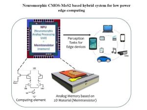
For example:
- Self-driving cars must make decisions instantly without waiting for cloud responses.
- Smart surveillance cameras need real-time object recognition.
- Wearable healthcare devices must continuously monitor vital signs with minimal battery drain.
- Industrial robots require rapid reactions in manufacturing environments.
Neuromorphic processors are particularly well-suited for these applications because they deliver near-zero latency and ultra-low power consumption.
Energy Efficiency and Sustainability
One of the biggest advantages of neuromorphic computing is energy efficiency. Conventional AI training and inference systems consume massive amounts of electricity. Data centers supporting generative AI models now require enormous cooling systems and power grids. Neuromorphic systems dramatically reduce this burden. According to recent studies, some neuromorphic architectures can achieve over 100 times better energy efficiency compared to traditional deep learning hardware.
The human brain itself consumes only about 20 watts of power — less than a dim light bulb — while performing tasks that remain challenging for modern computers. Neuromorphic engineers aim to approach this extraordinary level of efficiency. This has major implications for sustainable computing. As global AI adoption accelerates, reducing energy demand will become essential for lowering operational costs and minimizing environmental impact.
Real-World Applications
Neuromorphic Edge AI is already finding applications across multiple industries:
Healthcare
Wearable devices powered by neuromorphic chips can continuously monitor patient conditions, detect abnormalities, and even predict medical emergencies with minimal battery usage.
Autonomous Vehicles
Self-driving systems require split-second decisions. Neuromorphic processors enable rapid sensor processing for safer navigation and collision avoidance.
Robotics
Robots equipped with brain-inspired AI can react more naturally to changing environments while consuming far less energy.
Defense and Aerospace
Low-power edge computing is critical for drones, radar systems, and satellites operating in remote environments.
Consumer Electronics
Future smartphones, AR glasses, and smart home devices may run advanced AI locally without depending heavily on cloud services.
Challenges Ahead
Despite its promise, neuromorphic computing is still in its early stages. Developing efficient training methods for spiking neural networks remains difficult, and software ecosystems are less mature than traditional AI frameworks. Manufacturing specialized hardware at scale is another challenge. However, rapid advances in semiconductor technology and growing demand for sustainable AI are accelerating innovation in this field.
Conclusion
Neuromorphic Engineering and Edge AI represent a major shift in the future of computing. By mimicking the brain’s architecture, these technologies enable intelligent devices that are faster, smarter, and far more energy efficient than traditional systems. As AI continues to expand into every aspect of daily life, neuromorphic chips could become the foundation for a new generation of sustainable, low-latency, and autonomous technologies. The future of AI may no longer reside solely in giant cloud data centers — it may live directly inside the devices we use every day.
The post Neuromorphic Engineering & Edge AI: The Future of Intelligent Computing appeared first on ELE Times.
Ensuring Reliable AI in Safety-Critical Systems: Challenges and Engineering Solutions
In safety-critical environments, reliability is paramount, and errors have immediate, real-world consequences. If an autonomous system falters in urgent decisions, a clinical support tool misguides diagnoses, or an industrial controller fails in hazardous conditions, the results can be life-threatening. Artificial intelligence must be unwaveringly accurate and reliable at every moment to ensure safety and maintain trust in deployment.
This demands a fundamental shift in AI system engineering. Unlike traditional domains, where model accuracy or benchmark performance may suffice, safety-critical applications require predictable, consistent, and fail-aware behaviour across diverse conditions. The real challenge is to establish AI as fundamentally trustworthy in situations where failure is not an option, making reliability, not just intelligence, the core success criterion.
As AI integrates into mission-critical infrastructure, reliability is not just a technical requirement; it is the foundation and defining goal for deploying AI in safety-critical systems.
The Reliability Gap: From Probabilistic Models to Deterministic ExpectationsA core engineering challenge now demands urgent attention: a deep mismatch exists between traditional system design and modern AI behaviour. Safety-critical systems have historically been deterministic, producing predictable and verifiable outputs. In stark contrast, AI models are inherently probabilistically trained on data, influenced by variability, and alarmingly sensitive to environmental changes.
This mismatch creates a reliability gap that cannot be ignored in high-stakes deployments:
- High accuracy does not ensure safe behaviour in rare or unseen scenarios
- Models may generate confident yet incorrect predictions
- Behaviour under edge conditions remains difficult to anticipate
In safety-critical contexts, such uncertainties quickly become intolerable. Systems must now be engineered not just for performance, but for rigorous assurance under uncertainty. As Sundar Pichai warned, “The more capable AI becomes, the more critical it is to ensure it behaves safely and predictably.” This is no longer a theoretical challenge; it is the defining engineering crisis of our time.
Core Challenges in Deploying Reliable AI SystemsThe dynamic nature of real-world environments directly undermines reliability. AI systems trained in controlled settings inevitably confront distribution shifts at deployment scenarios absent from training data. These shifts degrade performance, especially in rare or safety-critical contexts.
In addition to distribution shifts, another critical issue is the inability of many models to communicate uncertainty. AI systems often produce outputs with high confidence, even when operating outside their domain of competence. In applications involving autonomous control or real-time decision-making, such overconfidence can lead to unsafe outcomes without warning.
Building on the previous concern, explainability is equally important. Safety-critical systems demand traceability and accountability, yet many AI models function as opaque decision-makers. Without the ability to interpret decisions, validating system behaviour and meeting regulatory expectations becomes significantly more difficult.
Finally, AI systems do not operate in isolation. They are part of a broader ecosystem involving sensors, embedded hardware, and control systems. Variability at any of these levels, whether due to sensor noise, latency, or hardware constraints, can influence overall system reliability. Ensuring dependable operation, therefore, requires a holistic, system-level perspective.
When AI Fails: Understanding System-Level RiskFailures in safety-critical AI systems are rarely isolated events. A single incorrect output can propagate across the system, leading to cascading effects that compromise overall functionality.
The most critical risks include:
- Silent failures, where incorrect outputs remain undetected
- Error propagation across interconnected system components
- Over-reliance on AI outputs, reducing effective human oversight
These risks highlight a key engineering principle: reliability must be designed into the system from the outset. It cannot be treated as a post-deployment evaluation metric.
Engineering Reliable AI: From Models to SystemsWe must shift from model-centric development to system-level assurance to address these challenges. We need to embed reliability across the entire lifecycle, from data collection to deployment and monitoring.
A foundational step is robust data engineering. Expand datasets to capture real-world variability. Simulate edge-case scenarios. Continuously monitor for data drift. These approaches improve generalisation and reduce unexpected system behaviour.
Equally important is uncertainty-aware system development. Integrate mechanisms that estimate prediction confidence so that models detect when they exceed their limits. This enables fallback strategies, like deferring to human operators or switching to safe modes. In this way, AI evolves from static prediction to self-aware system components.
Validation methodologies must also evolve. Traditional testing approaches are insufficient for capturing the complexity of AI behaviour. Scenario-based testing, simulation of rare or hazardous conditions, and stress testing under extreme inputs are becoming essential tools for evaluating reliability beyond standard datasets.
Explainability strengthens system assurance. While full transparency is rare, interpretable insights enable debugging, validation, and regulatory compliance. These capabilities help build trust among stakeholders.
Redundancy plays a central role in ensuring reliability. Instead of relying on a single model, systems increasingly incorporate multiple validation layers, hybrid architectures combining AI with rule-based logic, and predefined fail-safe states. As Satya Nadella emphasises, “Trust must be built into every layer of AI systems.” Redundancy ensures that this trust does not depend on a single point of failure.
System-Level Assurance: Beyond the AlgorithmA key realisation in modern engineering is that AI reliability cannot be isolated to the model alone. True assurance requires coordination across the entire system stack, including data pipelines, inference mechanisms, hardware platforms, and control logic.
This has led to the emergence of hardware-software co-design, where AI models are optimised alongside the systems that execute them. In this paradigm, reliability becomes a property of the entire system rather than an attribute of the algorithm alone.
Industry Perspective: Measured Adoption in High-Stakes DomainsAI adoption in safety-critical industries is cautious, driven by the persistent gap between experimental results and proven, production-level reliability.
Organisations are prioritising validation, risk mitigation, and incremental integration over rapid deployment. Hybrid approaches combining AI capabilities with deterministic safeguards are becoming increasingly common, reflecting the need to balance innovation with operational safety.
Regulatory and Certification ChallengesRegulatory frameworks for safety-critical systems were originally designed for deterministic software. Applying these frameworks to AI introduces significant challenges, particularly in verifying non-deterministic behaviour and defining acceptable risk thresholds.
The absence of standardised validation methodologies further complicates certification processes. As a result, the industry is moving toward new assurance models that emphasise transparency, traceability, and continuous validation throughout the system lifecycle.
Future Outlook: Toward Assured and Certifiable AIThe future of AI in safety-critical systems demands convergence. Data-driven intelligence will be fused with rule-based safeguards, and machine learning models will be integrated decisively with formal verification techniques.
Building on this convergence, continuous monitoring and adaptive system design will decisively enhance reliability, ensuring systems respond dynamically to changing conditions. We will deliver not just intelligent systems, but AI that is verifiably safe and certifiable for deployment.
As Jensen Huang states, “AI is advancing rapidly, but reliability and safety must scale with it.” This balance will define the next phase of AI engineering.
Conclusion: Reliability as the Foundation of Trustworthy AIAs AI expands into safety-critical domains, the definition of success is being redefined. Performance alone is no longer sufficient. Systems must demonstrate predictable behaviour under uncertainty, transparency in decision-making, and resilience in the face of failure.
AI must be engineered as a dependable system component, fully integrated into a broader safety and assurance framework. In this evolving landscape, reliability is not an added feature; it is the foundation upon which trust is built.
The trajectory of AI in safety-critical systems hinges not just on intelligence, but on how reliably these systems earn trust when it matters most.
The post Ensuring Reliable AI in Safety-Critical Systems: Challenges and Engineering Solutions appeared first on ELE Times.
Nanometer Nanotubes for Future Electronics
Researchers in Japan creates the world’s smallest semiconducting nanotubes, structures 100,000 times thinner than a human hair. By growing molybdenum disulfide inside protective tubes of boron nitride, researchers, including those from the University of Tokyo, produce highly uniform tubes just 1 nanometer wide, a scale at which it’s difficult to make stable nanotube structures. The work confirms decades-old theoretical predictions about how these ultrafine materials behave and could also provide a new route toward miniaturized electronic devices.
A few years back, carbon nanotubes were attracting a lot of press attention. But there’s a new contender in the ring, and it offers some advantages over its carbon counterpart that could tempt engineers to design products around it. Molybdenum disulfide (MoS2) nanotubes, though still experimental in nature, point to applications in semiconductor electronics, high-resolution sensing, and quantum-scale physics research.
“We achieved the synthesis of atomically precise semiconducting nanotubes with nanometer diameters. The coaxial structure, where a semiconducting MoS2 nanotube is surrounded by an insulating boron nitride (BN) nanotube, is attractive for gate-all-around transistors, one of the most advanced transistor architectures,” said Associate Professor Yusuke Nakanishi from the Department of Advanced Materials Science at the University of Tokyo. “Our paper demonstrates a way for structural control of inorganic semiconducting nanotubes at the atomic scale. And we experimentally demonstrated that the bandgap (related to how materials work as semiconductors) of the nanotubes decreases as their diameters become smaller, in agreement with theoretical predictions proposed more than a quarter century ago.”
Conventional methods for producing nanotubes are usually limited to diameters above 10 nanometers, multiwall concentric tubes, and poorly controlled or irregular atomic structures. Nakanishi and his team synthesized 1-nanometer-wide, single-wall MoS2 nanotubes with well-defined atomic structures. It manages the use of chemical reactions inside the narrow space of BN nanotubes. The confined space constrains the MoS2 nanotubes, which would otherwise be difficult to form, and promotes well-defined atomic arrangements, essential for engineered applications.
“In nanotubes, even small structural differences can strongly affect their properties. If the structure can be precisely controlled, the properties are more consistent, which is essential for reliable and reproducible transistor performance. Their biggest advantage is atomic-level structural control,” said Nakanishi. “Current silicon transistors are typically made by etching bulk silicon, but it’s increasingly difficult to keep their structures perfect at smaller sizes, where defects have a big impact. Carbon nanotubes also face a challenge for transistor applications, since even tiny structural differences can change how they behave, including whether they act more like metals or semiconductors. Our nanotubes could offer a more reliable way to build ultrasmall semiconductor channels with consistent properties.”
Practical applications are likely still some years away, and important challenges remain before working transistor devices can be made. In particular, the team wishes to increase the nanotube length from the current limit of several hundred nanometers to around 1 micrometer (which is 1,000 nanometers, and one-thousandth of a millimeter). Another future direction relates to materials: The method could also enable other inorganic nanotubes, including magnetic and superconducting materials. The researchers hope the work will help expand nanotube science beyond carbon-based systems and open the door to a broader class of atomically accurate nanotube materials for research, sensing, and smaller, faster devices.
The post Nanometer Nanotubes for Future Electronics appeared first on ELE Times.
Scientists discover a Quantum Effect that Eliminate Batteries
Tiny defects inside a quantum material may hold the key to battery-free electronics powered by energy already floating around us. Credit: AI/ScienceDaily.com Scientists have uncovered a new way to control an unusual quantum phenomenon that could one day help power electronic devices without batteries.
An international research team led by Professor Dongchen Qi from the Queensland University of Technology (QUT) School of Chemistry and Physics and Professor Xiao Renshaw Wang from Nanyang Technological University in Singapore investigated the physics behind the nonlinear Hall effect (NLHE), a quantum phenomenon with significant potential for future energy-harvesting technologies.
Unlike the classical Hall effect, the NLHE can convert alternating electrical signals directly into direct current. This means energy from wireless transmissions or other ambient sources could potentially be transformed into usable electricity without relying on conventional diodes or other bulky electronic components. The NLHE is a sophisticated quantum phenomenon in condensed matter physics where a voltage is generated perpendicular to an applied alternating current, even in the absence of a magnetic field, Professor Qi said.
“This effect allows us to convert alternating signals straight into direct current, which is what’s needed to power electronic devices. In principle, it means sensors or chips that could operate without batteries, drawing energy from their environment.”
Quantum Material Shows Stable Performance at Room Temperature
To better understand how the effect works, the researchers examined a high-quality topological material known for its unusual electronic behavior. Their experiments showed that the nonlinear Hall effect remains stable even at room temperature, an important step toward practical applications outside the laboratory. The team also discovered that temperature plays a key role in determining both the strength and direction of the electrical voltage produced by the material.
How Defects and Atomic Vibrations Control the Effect
At lower temperatures, tiny imperfections within the material had the greatest influence on the quantum effect. As temperatures increased, naturally occurring vibrations in the crystal structure became more important. This shift caused the direction of the generated electrical signal to reverse, revealing a previously unseen mechanism for controlling the phenomenon.
“Once you understand what’s happening inside the material, you can design devices to take advantage of it,” Professor Qi said.
That’s when quantum effects stop being abstract and start becoming useful — supporting future applications ranging from self-powered sensors and wearable technology to ultra-fast components for next-generation wireless networks. The findings provide new insight into how quantum materials behave and could help researchers develop smaller, faster, and more energy-efficient technologies that harvest power from their surroundings.
The post Scientists discover a Quantum Effect that Eliminate Batteries appeared first on ELE Times.
India’s Electronics Boost: SMT Expansion & Strategic Localization
India’s electronics manufacturing and design ecosystem marks a major infrastructure milestone with the inauguration of VVDN Technologies’ state-of-the-art Surface Mount Technology (SMT) line and Mechanical Innovation Park in Manesar. The launch highlights a broader structural shift in the nation’s industrial capacity, driven by targeted policy frameworks like the Make in India initiative.
According to data shared by Electronics and IT Minister Ashwini Vaishnaw during the deployment event, the sector’s manufacturing output has scaled fivefold over the last decade. This production surge is closely paired with an aggressive outward trade trajectory; electronics exports scaled six times over the same ten-year period, officially crossing the ₹3,25,000 crore threshold.
Deepening the Component Ecosystem
To transition from system-level assembly to deep-tech component localization, the government recently greenlit a dedicated electronic component manufacturing scheme. This policy framework is engineered to structurally mature the domestic supply chain, mitigate dependencies on imported sub-assemblies, and catalyze industrial workforce expansion. Currently, the electronics manufacturing sector accounts for an employment base of approximately 25 lakh individuals.
IP Safeguards and Supply Chain Resilience
Minister Vaishnaw emphasized that international hardware brands are increasingly anchoring their production pipelines in India due to two main technical and regulatory pillars:
- Enhanced Product Quality Standards: Rising yields and tighter quality control metrics across domestic fabrication and assembly lines.
- Robust Intellectual Property (IP) Safeguards: Tighter legal and technical frameworks protecting proprietary design architectures.
The state’s forward-looking roadmap relies on an integrated stack combining design-led innovation, manufacturing scaling, specialized technical skilling, and trusted hardware innovation. To secure long-term operational resilience against global market disruptions, India is actively focusing on securing diverse rare earth supply chains, establishing a trusted hardware baseline anchored tightly to IP protection and advanced engineering.
The post India’s Electronics Boost: SMT Expansion & Strategic Localization appeared first on ELE Times.
Сторінки

