
ELE Times

ElevateX 2026, Marking a New Chapter in Human Centric and Intelligent Automation
Teradyne Robotics today hosted ElevateX 2026 in Bengaluru – its flagship industry forum bringing together Universal Robots (UR) and Mobile Industrial Robots (MiR) to spotlight the next phase of human‑centric, collaborative, and intelligent automation shaping India’s manufacturing and intralogistics landscape.
Designed as a high‑impact platform for industry leadership and ecosystem engagement, ElevateX 2026 convened 25+ CEO/CXO leaders, technology experts, startups, and media, reinforcing how Indian enterprises are progressing from isolated automation pilots to scalable, business‑critical deployments. Ots)
Teradyne Robotics emphasized the rapidly expanding role of flexible and intelligent automation in enabling enterprises to scale confidently and safely. With industrial collaborative robots (cobots) and autonomous mobile robots (amr’s) becoming mainstream across sectors, the company underlined its commitment to driving advanced automation, skill development, and stronger industry‑partner ecosystems in India.
The event showcased several real‑world automation applications featuring cobots and amr’s across key sectors, including Automotive, F&B, FMCG, Education, and Logistics. These demos highlighted the ability of Universal Robots and MiR to help organizations scale quickly, redeploy easily, and improve throughput and workforce efficiency.
Showcasing high‑demand applications from palletizing and welding to material transport, machine tending, and training, the demonstrations reflected how Teradyne Robotics enables faster ROI, simpler deployment, and safe automation across high‑mix and high‑volume operations.
Speaking at the event, James Davidson, Chief Artificial Intelligence Officer, Teradyne Robotics, said, “Automation is entering a defining era – one where intelligence, flexibility, and human-centric design are no longer optional, but fundamental to how businesses innovate, scale, and compete. AI is transforming robots from tools that simply execute tasks into intelligent collaborators that can perceive, learn, and adapt in dynamic environments. In India, we are witnessing a decisive shift from experimentation to enterprise-wide adoption, and ElevateX 2026 reflects this momentum – bringing the ecosystem together to explore how collaborative and intelligent automation can become a strategic growth engine for both established enterprises and the next generation of startups.”
Poi Toong Tang, Vice President of Sales, Asia Pacific, Teradyne Robotics, added, “India is rapidly emerging as one of the most important and dynamic automation markets in Asia Pacific. Organizations today are not just looking to automate – they are looking to build operations that are flexible, resilient, and future-ready. The demand is for modular automation that delivers faster ROI and can evolve alongside business needs. Through Universal Robots and MiR, we are enabling end-to-end automation across production and intralogistics, helping Indian companies scale with confidence and compete on a global stage.”
Sougandh K.M., Business Director – South Asia, Teradyne Robotics, said, “India’s automation journey will be defined by collaboration across its ecosystem — by partners, system integrators, startups, and skilled talent working together to turn technology into real impact. At Teradyne Robotics, our belief is simple: automation should be for anyone and anywhere, and robots should enable people to do better work, not work like robots. Our focus is on automating tasks that are dull, dirty, and dangerous, while helping organizations improve productivity, safety, and quality. ElevateX 2026 is about lowering barriers to adoption and building long-term capability in India, making automation practical, scalable, and accessible, and positioning Teradyne Robotics as a trusted partner in every stage of that growth journey .”
Customer Case Story Testimonial/Teaser
A key highlight of ElevateX 2026 was the spotlight on customer success, and Origin stood out. As a fast‑growing U.S. construction tech startup, they shared how partnering with Universal Robots is driving measurable impact through improved productivity, stronger safety, and consistently high‑quality project outcomes powered by collaborative automation.
Yogesh Ghaturle, the Co-founder and CEO of Origin, said, “Our goal is to bring true autonomy to the construction site, transforming how the world builds. Executing this at scale requires a technology stack where every component operates with absolute predictability. Universal Robots provides the robust, operational backbone we need. With their cobots handling the mechanical precision, we are free to focus on deploying our intelligent systems in the real world.”
The post ElevateX 2026, Marking a New Chapter in Human Centric and Intelligent Automation appeared first on ELE Times.
The Architecture of Edge Computing Hardware: Why Latency, Power and Data Movement Decide Everything
Courtesy: Ambient Scientific
Most explanations of edge computing hardware talk about devices instead of architecture. They list sensors, gateways, servers and maybe a chipset or two. That’s useful for beginners, but it does nothing for someone trying to understand how edge systems actually work or why certain designs succeed while others bottleneck instantly.
If you want the real story, you have to treat edge hardware as a layered system shaped by constraints: latency, power, operating environment and data movement. Once you look at it through that lens, the category stops feeling abstract and starts behaving like a real engineering discipline.
Let’s break it down properly.
What edge hardware really is when you strip away the buzzwords
Edge computing hardware is the set of physical computing components that execute workloads near the source of data. This includes sensors, microcontrollers, SoCs, accelerators, memory subsystems, communication interfaces and local storage. It is fundamentally different from cloud hardware because it is built around constraints rather than abundance.
Edge hardware is designed to do three things well:
- Ingest data from sensors with minimal delay
- Process that data locally to make fast decisions
- Operate within tight limits for power, bandwidth, thermal capacity and physical space
If those constraints do not matter, you are not doing edge computing. You are doing distributed cloud.
This is the part most explanations skip. They treat hardware as a list of devices rather than a system shaped by physics and environment.
The layers that actually exist inside edge machines
The edge stack has four practical layers. Ignore any description that does not acknowledge these.
- Sensor layer: Where raw signals are produced. This layer cares about sampling rate, noise, precision, analogue front ends and environmental conditions.
- Local compute layer: Usually MCUs, DSP blocks, NPUs, embedded SoCs or low-power accelerators. This is where signal processing, feature extraction and machine learning inference happen.
- Edge aggregation layer: Gateways or industrial nodes that handle larger workloads, integrate multiple endpoints or coordinate local networks.
- Backhaul layer: Not cloud. Just whatever communication fabric moves selective data upward when needed.
These layers exist because edge workloads follow a predictable flow: sense, process, decide, transmit. The architecture of the hardware reflects that flow, not the other way around.
Why latency is the first thing that breaks and the hardest thing to fix
Cloud hardware optimises for throughput. Edge hardware optimises for reaction time.
Latency in an edge system comes from:
- Sensor sampling delays
- Front-end processing
- Memory fetches
- Compute execution
- Writeback steps
- Communication overhead
- Any DRAM round-trip
- Any operating system scheduling jitter
If you want low latency, you design hardware that avoids round-trip to slow memory, minimises driver overhead, keeps compute close to the sensor path and treats the model as a streaming operator rather than a batch job.
This is why general-purpose CPUs almost always fail at the edge. Their strengths do not map to the constraints that matter.
Power budgets at the edge are not suggestions; they are physics
Cloud hardware runs at hundreds of watts. Edge hardware often gets a few milliwatts, sometimes even microwatts.
Power is consumed by:
- Sensor activation
- Memory access
- Data movement
- Compute operations
- Radio transmissions
Here is a simple table with the numbers that actually matter.
| Operation | Approx Energy Cost |
| One 32-bit memory access from DRAM | High tens to hundreds of pJ |
| One 32-bit memory access from SRAM | Low single-digit pJ |
| One analogue in memory MAC | Under 1 pJ effective |
| One radio transmission | Orders of magnitude higher than compute |
These numbers already explain why hardware design for the edge is more about architecture than brute force performance. If most of your power budget disappears into memory fetches, no accelerator can save you.
Data movement: the quiet bottleneck that ruins most designs
Everyone talks about computing. Almost no one talks about the cost of moving data through a system.
In an edge device, the actual compute is cheap. Moving data to the compute is expensive.
Data movement kills performance in three ways:
- It introduces latency
- It drains power
- It reduces compute utilisation
Many AI accelerators underperform at the edge because they rely heavily on DRAM. Every trip to external memory cancels out the efficiency gains of parallel compute units. When edge deployments fail, this is usually the root cause.
This is why edge hardware architecture must prioritise:
- Locality of reference
- Memory hierarchy tuning
- Low-latency paths
- SRAM-centric design
- Streaming operation
- Compute in memory or near memory
You cannot hide a bad memory architecture under a large TOPS number.
Architectural illustration: why locality changes everything
To make this less abstract, it helps to look at a concrete architectural pattern that is already being applied in real edge-focused silicon. This is not a universal blueprint for edge hardware, and it is not meant to suggest a single “right” way to build edge systems. Rather, it illustrates how some architectures, including those developed by companies like Ambient Scientific, reorganise computation around locality by keeping operands and weights close to where processing happens. The common goal across these designs is to reduce repeated memory transfers, which directly improves latency, power efficiency, and determinism under edge constraints.
 Figure: Example of a memory-centric compute architecture, similar to approaches used in modern edge-focused AI processors, where operands and weights are kept local to reduce data movement and meet tight latency and power constraints.
How real edge pipelines behave, instead of how diagrams pretend they behave
Edge hardware architecture exists to serve the data pipeline, not the other way around. Most workloads at the edge look like this:
- The sensor produces raw data
- Front end converts signals (ADC, filters, transforms)
- Feature extraction or lightweight DSP
- Neural inference or rule-based decision
- Local output or higher-level aggregation
If your hardware does not align with this flow, you will fight the system forever. Cloud hardware is optimised for batch inputs. Edge hardware is optimised for streaming signals. Those are different worlds.
This is why classification, detection and anomaly models behave differently on edge systems compared to cloud accelerators.
The trade-offs nobody escapes, no matter how good the hardware looks on paper
Every edge system must balance four things:
- Compute throughput
- Memory bandwidth and locality
- I/O latency
- Power envelope
There is no perfect hardware. Only hardware that is tuned to the workload.
Examples:
- A vibration monitoring node needs sustained streaming performance and sub-millisecond reaction windows
- A smart camera needs ISP pipelines, dedicated vision blocks and sustained processing under thermal pressure
- A bio signal monitor needs to be always in operation with strict microamp budgets
- A smart city air node needs moderate computing but high reliability in unpredictable conditions
None of these requirements match the hardware philosophy of cloud chips.
Where modern edge architectures are headed, whether vendors like it or not
Modern edge workloads increasingly depend on local intelligence rather than cloud inference. That shifts the architecture of edge hardware toward designs that bring compute closer to the sensor and reduce memory movement.
Compute in memory approaches, mixed signal compute block sand tightly integrated SoCs are emerging because they solve edge constraints more effectively than scaled-down cloud accelerators.
You don’t have to name products to make the point. The architecture speaks for itself.
How to evaluate edge hardware like an engineer, not like a brochure reader
Forget the marketing lines. Focus on these questions:
- How many memory copies does a singleinference require
- Does the model fit entirely in local memory
- What is the worst-case latency under continuous load
- How deterministic is the timing under real sensor input
- How often does the device need to activate the radio
- How much of the power budget goes to moving data
- Can the hardware operate at environmental extremes
- Does the hardware pipeline align with the sensor topology
These questions filter out 90 per cent of devices that call themselves edge capable.
The bottom line: if you don’t understand latency, power and data movement, you don’t understand edge hardware
Edge computing hardware is built under pressure. It does not have the luxury of unlimited power, infinite memory or cool air. It has to deliver real-time computation in the physical world where timing, reliability and efficiency matter more than large compute numbers.
If you understand latency, power and data movement, you understand edge hardware. Everything else is an implementation detail.
The post The Architecture of Edge Computing Hardware: Why Latency, Power and Data Movement Decide Everything appeared first on ELE Times.
Govt Bets Big on Chips: India Semiconductor Mission 2.0 Gets ₹1,000 Crore Funding
In a significant push for the nation’s tech ambitions, the Government of India has earmarked Rs. 1,000 crores for the India Semiconductor Mission (ISM) 2.0 in the Union Budget 2026-27.
The new funding aims to supercharge domestic production, with investments slated for semiconductor manufacturing equipment, local IP development, and supply chain fortification both within India and on the international stage.
This upgraded version of the ISM will focus on industry-driven research and the refinement of training centres to enhance technology advancement, thereby fostering a skilled workforce for the future growth of the industry.
With India aiming for self-reliance through boosting domestic manufacturing in multiple sectors, the need for semiconductor manufacturing has exponentially increased.
Recently, Qualcomm tapped out the most advanced 2nm chips led by Indian engineering teams. This is a major boost to Indian semiconductor aspirations.
The first phase of the ISM was supported by a Rs. 76,000 crores incentive scheme, with ten projects worth Rs. 1.60 lakh crores approved by December, 2025, covering the entire manufacturing spectrum from fabrication units, packaging to assembly, and testing infrastructure development.
By: Shreya Bansal, Sub-editor
The post Govt Bets Big on Chips: India Semiconductor Mission 2.0 Gets ₹1,000 Crore Funding appeared first on ELE Times.
Microchip and Hyundai Collaborate, Exploring 10BASE-T1S SPE for Future Automotive Connectivity
The post Microchip and Hyundai Collaborate, Exploring 10BASE-T1S SPE for Future Automotive Connectivity appeared first on ELE Times.
Microchip Extends its Edge AI Solutions for Development of Production-ready Applications using its MCUs & MPUs
A major next step for artificial intelligence (AI) and machine learning (ML) innovation is moving ML models from the cloud to the edge for real-time inferencing and decision-making applications in today’s industrial, automotive, data center and consumer Internet of Things (IoT) networks. Microchip Technology has extended its edge AI offering with full-stack solutions that streamline the development of production-ready applications using its microcontrollers (MCUs) and microprocessors (MPUs) – the devices that are located closest to the many sensors at the edge that gather sensor data, control motors, trigger alarms and actuators, and more.
Microchip’s products are long-time embedded-design workhorses, and the new solutions turn its MCUs and MPUs into complete platforms for bringing secure, efficient and scalable intelligence to the edge. The company has rapidly built and expanded its growing, full-stack portfolio of silicon, software and tools that solve edge AI performance, power consumption and security challenges while simplifying implementation.
“AI at the edge is no longer experimental—it’s expected, because of its many advantages over cloud implementations,” said Mark Reiten, corporate vice president of Microchip’s Edge AI business unit. “We created our Edge AI business unit to combine our MCUs, MPUs and FPGAs with optimised ML models plus model acceleration and robust development tools. Now, the addition of the first in our planned family of application solutions accelerates the design of secure and efficient intelligent systems that are ready to deploy in demanding markets.”
Microchip’s new full-stack application solutions for its MCUs and MPUs encompass pre-trained and deployable models as well as application code that can be modified, enhanced and applied to different environments. This can be done either through Microchip’s embedded software and ML development tools or those from Microchip partners. The new solutions include:
- Detection and classification of dangerous electrical arc faults using AI-based signal analysis
- Condition monitoring and equipment health assessment for predictive maintenance
- Facial recognition with liveness detection supporting secure, on-device identity verification
- Keyword spotting for consumer, industrial and automotive command-and-control interfaces
Development Tools for AI at the Edge
Engineers can leverage familiar Microchip development platforms to rapidly prototype and deploy AI models, reducing complexity and accelerating design cycles. The company’s MPLAB X Integrated Development Environment (IDE) with its MPLAB Harmony software framework and MPLAB ML Development Suite plug-in provides a unified and scalable approach for supporting embedded AI model integration through optimised libraries. Developers can, for example, start with simple proof-of-concept tasks on 8-bit MCUs and move them to production-ready high-performance applications on Microchip’s 16- or 32-bit MCUs.
For its FPGAs, Microchip’s VectorBlox Accelerator SDK 2.0 AI/ML inference platform accelerates vision, Human-Machine Interface (HMI), sensor analytics and other computationally intensive workloads at the edge while also enabling training, simulation and model optimisation within a consistent workflow.
Other support includes training and enablement tools like the company’s motor control reference design featuring its dsPIC DSCs for data extraction in a real-time edge AI data pipeline, and others for load disaggregation in smart e-metering, object detection and counting, and motion surveillance. Microchip also helps solve edge AI challenges through complementary components that are required for product design and development. These include PCIe® devices that connect embedded compute at the edge and high-density power modules that enable edge AI in industrial automation and data centre applications.
The analyst firm IoT Analytics stated in its October 2025 market reportthat embedding edge AI capabilities directly into MCUs is among the top four industry trends, enabling AI-driven applications “…that reduce latency, enhance data privacy, and lower dependency on cloud infrastructure.” Microchip’s AI initiative reinforces this trend with its MCU and MPU platforms, as well as its FPGAs. Edge AI ecosystems increasingly require support for both software AI accelerators and integrated hardware acceleration on multiple devices across a range of memory configurations.
The post Microchip Extends its Edge AI Solutions for Development of Production-ready Applications using its MCUs & MPUs appeared first on ELE Times.
The Grid as Strategy: Powering India’s 2047 Transformation
by Varun Bhatia, Vice President – Projects and Learning Solutions, Electronics Sector Skills Council of India.
As India approaches its centenary in 2047, the idea of a Viksit Bharat has shifted decisively from aspiration to obligation. A 30 trillion-dollar economy, globally competitive manufacturing, integrated logistics, and digital universality are no longer distant goals. They are policy commitments.
Yet beneath every ambition lies a foundational truth. Development runs on dependable power. No country has crossed into developed-nation status on unreliable electricity. In India’s case, the transmission grid is not a supporting actor in this transformation. It is the stage itself.
The Grid That Holds the Nation Together
This transition from access to assurance has been enabled by a quiet but extraordinary expansion of India’s transmission network. India’s national power transmission system has crossed 5 lakh circuit kilometers, supported by 1,407 GVA of transformation capacity. Since 2014, the network has grown by 71.6 percent, with the addition of 2.09 lakh circuit kilometers of transmission lines and 876 GVA of transformation capacity. Integration at this scale has reshaped the energy landscape. The inter-regional power transfer capacity now stands at 1,20,340 megawatts, enabling electricity to move seamlessly across regions. This has successfully realized the vision of One Nation, One Grid, One Frequency and created one of the largest synchronized grids in the world. This architecture is not merely technical. It is economic infrastructure. It allows energy to flow from resource-rich states to industrial corridors without friction, strengthening productivity, investment confidence, and national competitiveness.
From Electrification to Excellence
India’s first power-sector revolution was about access, and that mission is largely complete. Saubhagya connected 2.86 crore households, while DDUGJY achieved universal village electrification by 2018. These were historic milestones.
However, access is only the starting point. Developed economies operate on a higher standard where power is always available, always stable, and always scalable. In a Viksit Bharat, outages must be exceptions rather than expectations. Voltage fluctuations cannot be built into business models. An industrial unit in rural Assam must receive the same quality of supply as one operating in an export hub in Southeast Asia. Reliability has now become the true benchmark of progress.
Rural India: From Load Centre to Growth Partner
The impact of a strong transmission backbone is most visible in rural India. Average rural power supply has increased from 12.5 hours per day in 2014 to 22.6 hours in FY 2025. This improvement has fundamentally altered the economic potential of villages and small towns. Reliability is being reinforced by systemic reforms. Under the Revamped Distribution Sector Scheme, grid modernization has reduced national AT&C losses to 15.37 percent, improving the financial sustainability of electricity supply.
Digital tools are accelerating this shift. More than 4.76 crore smart meters have been installed nationwide, bringing transparency, efficiency, and real-time control to energy consumption. Targeted interventions continue to close the remaining gaps. The PM-JANMAN initiative is electrifying remote habitations of Particularly Vulnerable Tribal Groups, while PM-KUSUM is reshaping agricultural power by enabling reliable daytime electricity through solarization. With states tendering over 20 gigawatts of feeder-level solar capacity, farmers are increasingly becoming urjadatas, contributing power back to the grid.
Reliable transmission makes this participation possible. The tower standing in a farmer’s field is no longer just infrastructure. It is a direct connection to the national economy. With assured round-the-clock power, industries no longer need to cluster around congested urban centers. Cold chains, food processing units, automated MSMEs, and digital services can operate efficiently in Tier-2 and Tier-3 towns. This urban transformation creates local employment, strengthens regional economies, and reduces migration pressures. In this model, rural India is no longer a subsidized consumer of power. It becomes a productive contributor to national growth.
Green Ambitions Need Grid Muscle
A Viksit Bharat must also be a sustainable Bharat. India’s commitment to achieving 500 gigawatts of non-fossil fuel capacity by 2030 reflects both climate responsibility and strategic foresight. Renewable energy, however, is geographically dispersed. Solar potential lies in deserts, wind along coastlines, and hydro resources in mountainous regions. Without a strong transmission backbone, clean energy remains stranded. The expanded grid, supported by investments under the Green Energy Corridor program, has become the central enabler of renewable integration. Strengthened inter-regional links ensure that clean power generated in remote areas can reach demand centers efficiently. This capability allows India to pursue growth without compromising its environmental commitments.
Resilience as National Security
Recent global energy shocks and climate-induced disruptions have reinforced one reality. Energy security is inseparable from national security. The grid of a developed India must therefore be resilient, intelligent, and adaptive. Smart Grids capable of self-healing, predictive maintenance, and advanced demand-response management are no longer optional. They are essential. Equally important is social resilience. Right-of-Way challenges require a partnership-driven approach. Landowners must be treated as stakeholders in national progress, with fair compensation and transparent processes that build trust and cooperation.
The Backbone of a Developed India
As India moves steadily toward 2047, development will be measured not only by economic output or industrial capacity, but by the consistency and quality of its power supply. Every kilometer of transmission line laid becomes a conduit for productivity. Every additional GVA of capacity strengthens energy security. The quiet hum of high-voltage lines signals a nation growing with confidence. Connecting Bharat is no longer about lighting homes. It is about powering aspirations, enabling enterprise, and securing India’s place as a self-reliant global force.
The transmission grid is not merely supporting the vision of Viksit Bharat. It is sustaining it.
The post The Grid as Strategy: Powering India’s 2047 Transformation appeared first on ELE Times.
Engineering the Future of High-Voltage Battery Management: Rohit Bhan on BMIC Innovation
ELE Times conducts an exclusive interview with Rohit Bhan, Senior Staff Electrical Engineer at Renesas Electronics America, discussing how advanced sensing, 120 V power conversion, ±5 mV precision ADCs, and ASIL D fault-handling capabilities are driving safer, more efficient, and scalable battery systems across industrial, mobility, and energy-storage applications.
Rohit Bhan has spent two decades advancing mixed-signal and system-level semiconductor design, with a specialization in AMS/DMS verification and battery-management architectures. Over the past year, he has expanded this foundation through significant contributions to high-voltage BMIC development, helping to push Renesas’ next generation of power-management solutions into new levels of accuracy, safety, and integration.
Rohit is highly regarded within Renesas and industry-wide for his ability to bridge detailed analog modeling, digital verification, and real-world application requirements. His recent work includes developing ±5 mV high-accuracy ADCs for precise cell monitoring, implementing an on-chip buck converter that reduces board complexity, and architecting 18-bit current-sensing solutions that enable more advanced state-of-charge and state-of-health analytics. He has also integrated microcontroller-driven safety logic into verification environments—supporting ASIL D-level fault detection and autonomous response—while contributing to Renesas’ first BMIC design.
Rohit’s expertise spans behavioral modeling, reusable verification environments, multi-cell chip operation, and stackable architectures for even higher cell counts. His end-to-end perspective—ranging from system definition and testbench development to customer engagement and product innovation—has made him a key contributor to Renesas’ battery-management roadmap. As the industry moves toward higher voltages, smarter analytics, and tighter functional-safety requirements, his work is helping shape the next wave of intelligent, reliable, and scalable BMIC platforms.
Here are the excerpts from the interaction:
ELE Times: Rohit, you recently helped deliver a multi-cell BMIC architecture capable of operating at high voltage. What were the most significant engineering hurdles in moving to a new process technology for the first time, and what does that enable for future high-voltage applications?
ROHIT BHAN: From a design perspective, key challenges included managing high-stress device margins (such as parasitic bipolar effects and field-plate optimization), defining robust protection strategies for elevated operating conditions, integrating higher-energy power domains, maintaining analog accuracy across very large common-mode ranges, and working through evolving process design kit maturity. From a verification standpoint, this required extensive coverage of extreme transient conditions (including electrical overstress, surge, and load-dump-like events), which drove expanded corner matrices, mixed-signal simulation complexity, and tight correlation between silicon measurements and models to close the accuracy loop and ensure specified performance.
Looking forward, these advances enable future high-energy applications with increased monitoring and protection headroom, simpler system-level implementations, and improved measurement integrity. A mature high-stress-capable process combined with robust analog and IP libraries provides a scalable foundation for derivative products (such as variants with different channel densities or feature sets) and for modular or isolated architectures that support higher aggregate operating ranges—while preserving a common verification, validation, and qualification framework.
ELE Times: Among your 2025 accomplishments, your team achieved ±5 mV accuracy in cell-voltage measurement. Why is this level of precision so critical for cell balancing, battery longevity, and safety—especially in EV, industrial, and energy-storage use cases?
RB: If our measurement error is ±20 mV, the BMIC can “think” a cell is high when it isn’t or miss a genuinely high cell; the result is oscillatory balancing and residual imbalance that never collapses. Tightening to ±5 mV allows thresholds and hysteresis to be set small enough that balancing actions converge to a narrow spread instead of dithering. Over hundreds of cycles, that cell becomes the pack limiter (early full/empty flags, rising impedance). Keeping the max cell delta small via ±5 mV metrology lowers the risk of one cell aging faster and dragging usable capacity and power down. In addition, early detection of abnormal dV/dt under load or rest hinges on accurate voltage plateaus and inflection points—errors here mask the onset of dangerous behavior.
ELE Times: An on-chip buck converter is a major milestone in integration. How did you approach embedding such a high-voltage converter into the BMIC, and what advantages does this bring to OEMs in terms of board simplification, thermal performance, and cost?
RB: There are multiple steps involved in making this decision. It starts with finding the right process and devices, partitioning the power tree into clean voltage domains, and engineering isolation, spacing, and ESD for HV switching nodes. Finally, close the control loop details (gate drive, peak‑current trims, offsets) and verify at the system level, and correlate early in the execution phase.
For OEMs, this translates into simpler boards with fewer external components, easier routing, and a smaller overall footprint, while eliminating the need for external high-stress pre-regulators feeding the battery monitor, since the pack-level domain is managed on die. By internalizing the high-energy conversion and using cleaner harnessing and creepage strategies, elevated-potential nodes are no longer distributed across the board, significantly simplifying creepage and clearance planning at the power-management boundary. The result is fewer late-stage compliance surprises and integrated high-energy domains that are aligned with process-level reliability reviews, reducing the risk of re-layout driven by spacing or derating constraints.
ELE Times: You also worked on an 18-bit ADC for current sensing. How does this resolution improve state-of-charge and state-of-health algorithms, and what new analytics or predictive-maintenance features become possible as a result?
RB: Regarding the native 18‑bit resolution and long integration window: the coulomb‑counter (CC) ADC integrates for ~250 ms (milliseconds) per cycle, with selectable input ranges ±50/±100/±200 mV across the sense shunt; results land in CCR[L/M/H] and raise a completion IRQ. This is the basis for low‑noise charge throughput measurement and synchronized analytics. Error and linearity you can budget: the EC table shows 18‑bit CC resolution, INL ~27 LSB, and range‑dependent µV‑level error (e.g., ±25 µV in the ±50 mV range), plus a programmable dead‑zone threshold for direction detection—so the math can be made deterministic. Cross‑domain sync: A firmware/RTL option lets the CC “integration complete” event trigger the voltage ADC sequencer, tightly aligning V and I snapshots for impedance/OCV‑coupled analytics.
Two main functionalities that depend on this accuracy are State of Charge (SOC) and State of Health (SOH). First, for SOC accuracy—following is where the extra bits show up:
- Lower quantization and drift in coulomb counting: with 18‑bit integration over 250 ms, the charge quantization step is orders smaller than typical load perturbations. Combined with the ±25–100 µV error bands (range‑dependent), which reduces cycle‑to‑cycle SOC drift and tightens coulombic efficiency computation—especially at low currents (standby, tail‑charge), where coarse ADCs mis‑estimate.
- Cleaner “merge” of model‑based and measurement‑based SOC: the synchronized CC‑→‑voltage trigger lets you fuse dQ/dV features with the integrated current over the same window, improving EKF/UKF observability when OCV slopes flatten near the top of charge. Practically: fewer recalibration waypoints and tighter SOC confidence bounds across temperature.
- Robust direction detection at very small currents: the dead‑zone and direction bits (e.g., cc_dir) are asserted based on CC codes exceeding a programmable threshold; you can reliably switch charge/discharge logic around near‑zero crossings without chattering. That matters for taper‑charge and micro‑leak checks.
For SOH + predictive maintenance, this resolution enables capacity‑fade trending with confidence, specifically:
- Cycle‑level coulombic efficiency becomes statistically meaningful, not noise‑dominated—letting you detect early deviations from the fleet baseline.
- Impedance‑based health scoring (per cell and stack): enabling impedance mode in CC (aligned with voltage sampling) gives snapshots each conversion period; tracking ΔR growth vs. temperature and SOC identifies aging cells and connector/cable degradation proactively.
- Micro‑leakage & parasitic load detection: with µV‑level CC error windows and long integration, you can flag slow, persistent current draw (sleep paths, corrosion) that would be invisible to 12–14‑bit chains—preventing “vanishing capacity” events in ESS and industrial packs.
- Adaptive balancing + charge policy: fusing accurate dQ with cell ΔV allows balancing decisions based on energy imbalance, not just voltage spread. That reduces balancing energy, speeds convergence, and lowers thermal stress on weak cells.
- Early anomaly signatures: the combination of high‑resolution CC and triggered voltage sequences yields load‑signature libraries (step response, ripple statistics) that expose incipient IR jumps or contact resistance growth—feeding an anomaly detector before safety limits trip.
ELE Times: Even with high-accuracy ADCs, on-chip buck converters, and advanced fault-response logic, the chip is designed to minimize quiescent current without compromising monitoring capability. What design strategies or architectural decisions enabled such low power consumption?
RB: We achieved very low standby power through four key strategies. First, we defined true power states that completely shut down high-consumption circuitry, such as switching regulators, charge pumps, high-speed clocks, and data converters. Second, wake-up behavior is fully event-driven rather than periodically active. Third, the always-on control logic is designed for ultra-low leakage operation. Finally, voltage references and regulators are aggressively gated, so precision analog blocks are only enabled when they are actively needed. Deeper low-power modes further reduce consumption by selectively disabling additional domains, enabling progressively lower leakage states for long-term storage or shipping scenarios.
ELE Times: You’ve emphasized the role of embedded microcontrollers in both chip functionality and verification. Can you explain how MCU-driven fault handling—covering short circuits, overcurrent, open-wire detection, and more—elevates functional safety toward ASIL D compliance?
RB: In our current chip, safety is layered so hazards are stopped in hardware while an embedded MCU and state machines deliver the diagnostics and control that raise integrity toward ASIL D. Fast analog protection shuts high‑side FETs on short‑circuit/overcurrent and keeps low‑frequency comparators active even in low‑power modes, while event‑driven wake and staged regulator control ensure deterministic, traceable transitions to safe states.
The MCU/FSM layer logs faults, latches status, applies masks, and cross‑checks control vs. feedback, with counters providing bounded detection latency and reliable classification—including near‑zero current direction via a programmable dead‑zone. Communication paths use optional CRC to guard commands/telemetry, and a dedicated runaway mechanism forces NORMAL→SHIP if software misbehaves, guaranteeing a known safe state. Together, these mechanisms deliver immediate hazard removal, high diagnostic coverage of single‑point/latent faults, auditable evidence, and controlled recovery—providing the system‑level building blocks needed to argue ISO 26262 compliance up to ASIL D.
ELE Times: Stackable BMICs are becoming a major focus for high-cell-count systems. What challenges arise when daisy-chaining devices for applications like e-bikes, industrial storage, or large EV packs, and how is your team addressing communication, synchronization, and safety requirements?
RB: Stacking BMICs for high‑cell‑count packs introduces tough problems—EMI and large common‑mode swings on long harnesses, chain length/topology limits, tighter protocol timing at higher baud rates, coherent cross‑device sampling, and ASIL D‑level diagnostics plus safe‑state behavior under hot‑plug and sleep/wake. We address these with hardened links (transformer for tens of meters, capacitive for short hops), controlled slew and comparator front‑ends, ring/loop redundancy, and ASIL D‑capable comm bridges that add autonomous wake; end‑to‑end integrity uses 16/32‑bit CRC, timeouts, overflow guards, and memory CRC. For synchronization, we enforce true simultaneous sampling, global triggers, and evaluate PTP‑style timing, using translator ICs to coordinate mixed chains.
ELE Times: You have deep experience building behavioral models using wreal and Verilog-AMS. How does robust modeling influence system definition, mixed-mode verification, and ultimately silicon success for high-voltage BMICs?
RB: Robust wreal/Verilog‑AMS modeling is a force multiplier across the mixed signal devices. It clarifies system definition (pin‑accurate behavioral blocks with explicit supplies, bias ranges, and built‑in checks), accelerates mixed‑mode verification (SV/UVM testbenches that reuse the same stimuli in DMS and AMS, with proxy/bridge handshakes for analog ramp/settling), and de‑risks silicon by catching integration and safety issues early (SOA/EMC assumptions, open‑wire/CRC paths, power‑state transitions) while keeping sims fast enough for coverage.
Concretely, pin‑accurate DMS/RNM models and standardized generators enforce the right interfaces and bias/inputs status (“supplyOK”, “biasOK”), reducing schematic/model drift. SV testbenches drive identical sequences into RNM and AMS configs for one‑bench reuse so timing‑critical behaviors are verified deterministically. RNM delivers order‑of‑magnitude speed‑ups (e.g., ~60× seen in internal comparisons) to reach coverage across modes. Model‑vs‑schematic flows quantify correlation (minutes vs. hours) and expose regressions when analog blocks change. Together with these practices in our methodology and testbench translates into earlier bug discovery, tighter spec alignment, and first‑time‑right outcomes.
ELE Times: Your work spans diverse categories—from power tools and drones to renewable-energy systems and electric mobility. How do application-specific requirements shape decisions around cell balancing, current sensing, and protection features?
RB: Across segments, application realities drive our choices: power tools and drones favor compact BOMs and fast transients, so 50 mA internal balancing with brief dwell and measurement settling, tight short‑circuit latency, and coulomb‑counter averaging for SoC works well; e‑bikes/LEV typically stay at 50 mA but require separate charge vs. discharge thresholds (regen vs. propulsion), longer DOC windows and microsecond‑class SCD cutoffs to satisfy controller safety timing. Industrial/renewables often need scheduled balancing and external FET paths beyond 50 mA, plus deep diagnostics (averaging, CRC, open‑wire) across daisy‑chained stacks and EV/high‑voltage packs push toward ASIL D architectures with pack monitors, redundant current channels, contactor drivers, and ring communications. Current sensing is chosen to match the environment—low‑side for cost‑sensitive packs, HV differential with isolation checks in EV/ESS—while an 18‑bit ΔΣ coulomb counter and near‑zero dead‑zone logic preserve direction fidelity. Protection consistently blends fast analog comparators for immediate energy removal with MCU‑logged recovery and robust comms (CRC, watchdogs), so each market gets the right balance of performance, safety, and serviceability.
ELE Times: As battery management and gauges (BMG) evolve toward higher voltages, embedded intelligence, and greater integration, what do you see as the next major leap in BMIC design? Where are the biggest opportunities for innovation over the next five years?
RB: This is an exciting topic. Based on our roadmaps and the work we have been doing, the next major leap in BMIC design is a shift from “cell‑monitor ICs” to a smart, safety‑qualified pack platform—a Battery Junction Box–centric architecture with edge intelligence, open high‑speed wired communications, and deep diagnostics that run in drive and park. Here’s where I believe the biggest opportunities lie over the next five years:
- Pack‑centric integration: the Smart Battery Junction Box
- Communications: from proprietary chains to open, ring‑capable PHY
- Metrology: precision sensing + edge analytics
- Functional safety that persists in sleep/park
- Power: HV buck integration becomes table stakes
- Balancing: thermal‑aware schedulers and scalable currents
- Cybersecurity & configuration integrity for packs
- Verification‑driven design: models that shorten the loop.
The post Engineering the Future of High-Voltage Battery Management: Rohit Bhan on BMIC Innovation appeared first on ELE Times.
Anritsu Launches New RF Hardware Option, Supporting 6G FR3
Anritsu Corporation released a new RF hardware option for its Radio Communication Test Station MT8000A to support the key FR3 (Frequency Range 3) frequency band for next‑gen 6G mobile systems. With this release, the MT8000A platform now supports evolving communications technologies, covering R&D through to final commercial deployment of 4G/5G and future 6G/FR3 devices.
Anritsu will showcase the new solution in its booth at MWC Barcelona 2026 (Mobile World Congress), the world’s largest mobile communications exhibition, held in Barcelona, Spain, from March 2 to 5, 2026.
Since 6G is expected to deliver ultra-high speed, ultra-low latency, ultra-safety and reliability far surpassing 5G, worldwide, international standardisation efforts are accelerating toward commercial 6G release.
The key high‑capacity data transmission and wide-coverage features of 6G require using the FR3 frequency band (7.125 to 24.25 GHz), and the Lower FR3 band range up to 16 GHz, which extends from the FR1 (7.125 GHz) band, is already on the agenda for the 2027 World Radiocommunication Conference (WRC-27) discussions.
By leveraging its long expertise in wireless measurement, Anritsu’s MT8000A test platform leads the industry with this highly scalable new RF hardware option supporting the Lower FR3 band, and covering both current and next‑generation technologies. Future 6G functions will be supported by seamless software upgrades, helping speed development and release of new 6G devices.
Development Background
The FR3 frequency band is increasingly important in achieving practical 6G devices, meaning current 4G/5G test instruments (supporting FR1 and FR2) require hardware upgrades.
Additionally, dedicated FR3 RF tests are required because FR3 and conventional FR1/FR2 bands have different RF-related connectivity and communication quality features.
Furthermore, FR3 test instruments will be essential for both 6G protocol tests to validate network connectivity, and for functional tests to comprehensively evaluate service/application performance.
These factors are driving demand for a highly expandable, multifunctional, and high‑performance test platform like the MT8000A, covering both existing 4G/5G devices and next‑generation multimode 4G/5G/6G devices.
Product Overview and Features
Radio Communication Test Station MT8000A
The current MT8000A test platform supports a wide range of 3GPP-based applications, including RF, protocol, and functional tests for developing 4G/5G devices.
By adding this new industry-beating RF hardware option supporting 6G/Lower FR3 bands, Anritsu’s MT8000A platform assures long‑term, cost-effective use for developing future 6G/FR3 devices.
Anritsu’s continuing support for future 6G/FR3 test functions using MT8000A software upgrades will advance the evolution of next‑generation communications and help achieve a useful, safe, and stable network‑connected society.
The post Anritsu Launches New RF Hardware Option, Supporting 6G FR3 appeared first on ELE Times.
Anritsu Achieves Skylo Certification to Accelerate Global Expansion for NTNs
ANRITSU CORPORATION announced the expansion of its collaboration with Skylo Technologies with the successful certification of Anritsu’s RF and protocol test cases for Skylo’s non-terrestrial network (NTN) specifications. This milestone completes a comprehensive suite of Skylo-approved RF and protocol test cases, enabling narrowband IoT devices to operate seamlessly over Skylo’s NTN in alignment with 3GPP Release 17.
The momentum behind satellite-to-ground connectivity continues to accelerate as mobile operators and enterprises seek to extend reliable coverage across remote regions, industrial sites, and maritime environments. Under these circumstances, Skylo’s NTN network brings efficient power, low cost, and highly resilient NB-IoT capabilities to industries such as agriculture, logistics, maritime, and mining, enabling remote sensing, asset tracking, and safety-critical applications where a terrestrial network is out of reach.
Using Anritsu’s ME7873NR and ME7834NR platforms, now certified under the Skylo Carrier Acceptance Test program, device manufacturers will be able to validate NB-IoT NTN chipsets, modules, and devices for Skylo’s network with a fully automated and repeatable test environment. These solutions integrate 3GPP 4G and 5G protocols with NTN-specific parameters, ensuring accurate simulation of live network scenarios while reducing test time and accelerating device readiness.
Anritsu’s test solutions provide end-to-end validation for terrestrial and non-terrestrial networks within a single environment, enabling realistic emulation of satellite channel conditions and orbital dynamics for comprehensive verification of device performance. This level of testing rigour ensures interoperability, reliability, and high performance for dual-mode NTN devices destined for deployment across global markets.
Andrew Nuttall, Chief Technology Officer and Co-founder at Skylo Technologies, said: “We’re excited to join forces with Anritsu to accelerate innovation in non-terrestrial networks. This collaboration strengthens our shared commitment to delivering reliable, high-performance connectivity solutions for a rapidly evolving global market. Together, we’re enabling the next generation of devices and services that will redefine what’s possible in satellite-enabled connectivity.”
Daizaburo Yokoo, General Manager of Anritsu’s Mobile Solutions Division, said: “Partnering with Skylo represents an exciting step forward in advancing non-terrestrial network technology. This collaboration underscores our shared commitment to drive interoperability and set new standards for the future of global communications.”
Skylo operates on 3GPP Release 17 specifications and has developed additional “Standards Plus” extensions to enhance performance and interoperability across satellite networks. These Skylo-specified enhancements ensure that devices certified through the Skylo CAT program deliver robust connectivity and a seamless user experience across its expanding NTN footprint.
In partnership with Skylo, Anritsu remains committed to advancing 5G device development, enabling seamless global connectivity for data, voice, and messaging.
The post Anritsu Achieves Skylo Certification to Accelerate Global Expansion for NTNs appeared first on ELE Times.
Arrow Electronics Initiates Support for Next-Gen Vehicle E/E Architecture
Arrow Electronics has launched a strategic initiative and research hub to support next-generation vehicle electrical and electronic (E/E) architecture.
The available resources provide automotive manufacturers and tier-1 suppliers with the engineering expertise and supply chain stability required to navigate the industry’s shift toward software-defined vehicles.
As consumer and commercial vehicles evolve into complex, intelligent platforms, the traditional method of adding a separate computer for every new electronic feature is no longer sustainable. E/E architecture represents a complete overhaul of the “nervous system” within modern vehicles.
This fundamental shift moves away from hundreds of individual components toward a more centralised system where powerful computing hubs manage multiple functions. This transition can streamline and harmonise systems and operations while reducing the internal wiring of a car by up to 20 per cent, leading to vehicles that are lighter, more energy-efficient and easier to update via software throughout the vehicle’s lifecycle.
Aggregating Hardware, Software and Supply Chain Expertise
Arrow is a central solution aggregator for E/E architecture, bridging the gap between individual components and complete, integrated systems. Arrow’s portfolio of design engineering services includes a dedicated team of automotive experts who provide cross-technology support in both semiconductor and IP&E (interconnect, passive and electromechanical components) sectors.
This technical depth is matched by a vast global inventory and robust supply chain services that help ensure confidence through multisourced, traceable component strategies and proactive obsolescence planning so that automakers have the right components in hand when they need them.
In addition to hardware, Arrow has significantly expanded its transportation software footprint in recent years to include expertise in AUTOSAR, functional safety standards and automotive cybersecurity.
Strengthening the Automotive Ecosystem
“E/E architecture is the cornerstone of the modern automotive revolution, enabling the transition from hardware-centric machines to intelligent, software-defined mobility,” said Murdoch Fitzgerald, chief growth officer of global services for Arrow’s global components business. “By combining our global engineering reach with a broad range of components and specialised software expertise, we are well positioned to help our customers navigate this complexity, reducing their time-to-market and helping ensure their platforms are built to adapt as the industry evolves.”
Arrow’s E/E architecture initiative builds on the company’s 2024 acquisitions of specialist software firms iQMine and Avelabs, leading engineering services providers for the automotive and transportation industry. These additions have bolstered Arrow’s software development centres and its Automotive Centre of Excellence.
To support engineers and procurement leaders through E/E architecture redesign, Arrow has launched a new dedicated research hub. This online resource provides comprehensive technical insights, whitepapers and design tools specifically for E/E architecture development.
The post Arrow Electronics Initiates Support for Next-Gen Vehicle E/E Architecture appeared first on ELE Times.
Software-Defined Everything: The Foundation of the AI-powered Digital Enterprise
Courtesy: Siemens
Industry today is not facing a single technological change but a structural transformation. Markets are evolving faster than production systems, product life cycles are shortening, while industrial assets are designed to last for decades. At the same time, complexity along the entire value chain is increasing – technologically, organizationally, and regulatory. In this reality, adaptability becomes the decisive capability to secure and sustainably develop industrial value creation.
Within this context, classical automation reaches its structural limits. Automation based on fixed sequences, static logics, and extensive manual engineering can no longer keep up with the pace of modern industry. Efficiency gains within this paradigm are insufficient when products, processes, and frameworks are constantly changing – and they do not provide a sustainable foundation for the widespread use of artificial intelligence.
What is needed now is the next evolutionary step: the automation of automation itself. Instead of specifying every process in detail, industrial systems must be empowered to solve tasks autonomously – based on objectives, context, and continuous learning. Software-Defined Everything (SDx) becomes the necessary organising principle: it decouples functionality from specific hardware, creates a continuous, lifecycle-spanning data foundation, and enables systems to self-configure, adapt, and optimise.
In production, this approach manifests as Software-Defined Automation (SDA). SDA is the consistent application of Software-Defined Everything to the production automation layer. Control logic, functionality, and intelligence are decoupled from physical hardware, software-defined, and continuously developed. Hardware remains the stable, high-performance foundation, while software provides flexibility, adaptability, and learning capability to production systems.
This creates the structural basis for the AI-powered Digital Enterprise: an industrial organisation in which software, digital twins, and industrial AI work in closed-loop cycles, systems learn continuously, and decisions are not only prepared but also operationally executed. From this capability, the path to the Industrial Metaverse opens up – as the next stage of development, where planning, simulation, collaboration, and operational control converge in a shared digital space, supporting real industrial value creation in real time.
Stable foundation, flexible control: Software-Defined Automation in production
For many years, industrial functionality was inseparably tied to hardware. New requirements meant new components, modifications, or downtime. This model was stable – but no longer fast enough.
Software-Defined Everything breaks this logic. Functions, intelligence, and control are decoupled from specific hardware and moved into software. In production, this takes the form of Software-Defined Automation (SDA): the automation layer itself becomes software-defined, controlled, and continuously improved, while hardware continues to serve as a stable, high-performance foundation.
This fundamentally changes industrial systems:
- Functions can be adapted via software instead of physical modifications
- Systems evolve continuously throughout their lifecycle
- Adaptability becomes a structural characteristic
Industry becomes not only more digital but also definable, controllable, and optimizable through software.
Practical example: Software-Defined Automation in action
How this transformation is already becoming reality can be seen in the automotive industry. Companies, together with Siemens, are implementing Software-Defined Automation as an integral part of Software-Defined Everything. By introducing a virtual, TÜV-certified PLC, production control logic is no longer tied to physical control hardware but runs as software – centrally managed, flexibly scalable, and continuously updated.
This implements a core principle of SDA: the automation layer itself is software-defined. New functions can be rolled out via software, production systems can be quickly adapted to new vehicle variants, and updates and tests can be prepared and validated virtually. IT and OT environments converge into a unified, software-based operation.
The result is production that is not only more efficient but also learning- and AI-capable – a key prerequisite for the AI-powered Digital Enterprise.
Software-Defined as a bridge between goal and reality
The real value of Software-Defined Everything lies not in individual applications but in connecting the digital target picture with actual operations. SDx – and in production specifically SDA – enables the digital representation of target and actual states of industrial systems and products.
Real operational data from running plants is combined with target states from simulations, digital twins, and engineering models. Unlike isolated analytics or digital twin solutions, this creates a continuous, consistent data foundation across the entire lifecycle – from design through implementation to optimisation. Most importantly, it creates a bidirectional connection: digital insights directly influence operations.
Digital insights are no longer abstract. They become actionable.
Why Software-Defined Everything is the prerequisite for Industrial AI
Artificial intelligence only delivers value in industry if it can do more than analyse – it must act. On a software-defined data foundation, target and operational states can be continuously compared and contrasted. AI methods detect deviations, identify correlations across products, machines, and plants, and derive concrete optimisation recommendations.
The decisive step follows: Software-Defined Everything – and in production, Software-Defined Automation – closes the loop. AI-driven insights are directly translated into operational adjustments. Machines, processes, and products respond autonomously, without manual reconfiguration.
This creates learning systems that continuously improve – not as an exception, but as the standard.
The AI-powered Digital Enterprise: Learning as an operating system
When Software-Defined Everything, Software-Defined Automation, digital twins, and industrial AI interact, a new form of industrial organisation emerges. Products become platforms, production systems dynamically adapt to new variants and requirements, and knowledge is generated in ongoing operations and systematically made usable.
The AI-powered Digital Enterprise is therefore not a static target but a continuous learning process embedded within the systems themselves.
Industrial Metaverse: The consequence of a Software-Defined reality
From this development, the Industrial Metaverse becomes tangible – not as a visualisation, but as a new operational and management layer. When digital twins accurately reflect the real state, when AI prepares or autonomously makes decisions, and when software directly translates these decisions into real-world actions, the virtual space becomes the central environment for planning, collaboration, and optimisation.
Software-Defined Everything as a structural capability
Software-Defined Everything – with Software-Defined Automation as the core for production – is not a short-term trend or an isolated technology choice. It is the structural prerequisite to make industrial systems learning-capable, adaptable, and future-proof, and to unlock the full potential of AI for the industry of the future.
The post Software-Defined Everything: The Foundation of the AI-powered Digital Enterprise appeared first on ELE Times.
3 semicon-enabled innovations impacting our experience of the world
Courtesy: Texas Instruments
The chips that power today’s smartphones contain over 15 billion transistors; the semiconductors powering data centres can have hundreds of billions of transistors. Semiconductors drive and power breakthroughs across hundreds of critical and emerging industries, such as robotics, personal electronics and artificial intelligence. As semiconductors continue to enable the world to function and make life more convenient and safer, their role will only increase.
The importance of chips – and the electronics they’re enabling – has been made possible by years of semiconductor progress. Let’s review how semiconductor technologies are enabling three innovations in electronics that impact how we experience the world.
Innovation No. 1: Systems that operate safely around humans
“You might think humanoids are 3 to 5 years away. But really, humanoids are the present,” said Giovanni Campanella, general manager of factory automation, motor drives and robotics at TI, at a Computex speech.
Humanoids’ emergence is anything but simple. Robots that perform chores in homes, complete tasks in a factory, or even clean dishes in a restaurant kitchen must adapt in dynamic environments, where things change every second.
In order to build adaptable robots that can operate around humans in diverse settings, such as domestic or business environments, design engineers must leverage semiconductor technologies. Each of these technologies must work together to perform the actions of one safe and functional humanoid. Actuators in robots enable their movements. With sensing, the robot can perceive its surrounding environment, and a central computer acts as its brain, analysing and making decisions from that sensing data. Communication with the compute units and actuators happens in real time, so the humanoid can complete a task, such as handing an object to someone.
Innovation No. 2: Smaller, more affordable, smarter devices
Smartphones and laptops keep getting thinner and lighter. Medical patches provide continuous monitoring without external equipment. Devices are on a trajectory to fit into an individual’s life, increasing convenience and accessibility.
How are designers able to continually progress toward the trend of “smaller” and more convenient when last year’s newest smartphone was already the smallest ever?
Significant advances in component design are enabling this progress. An example of this was our launch of the world’s smallest MCU, reflecting breakthroughs in packaging, integration and power efficiency that allow more functionality to fit into dramatically smaller spaces.
“With the addition of the world’s smallest MCU, our MSPM0 MCU portfolio provides unlimited possibilities to enable smarter, more connected experiences in our day-to-day lives,” said Vinay Agarwal, vice president and general manager of MSP Microcontrollers at TI.
Due to semiconductors, headphones that were once clunky can now fit into a pocket and provide a premium audio experience. Smart rings instantly track health metrics like activity and heart rate without interrupting everyday activities. With devices like the world’s smallest MCU, the prevalence of smaller, more affordable electronics that seamlessly blend into an already-existing routine is expanding.
Innovation No. 3: AI everywhere
By 2033, the global AI market is expected to account for $4.8 trillion – 25 times higher than the $189 billion valuation in 2023. AI is already enabling smartphones to process images in real time, cars to monitor drivers and their surroundings, and medical devices to deliver precise insights, and with its projected growth, the possibilities of where else AI can appear seem endless.
But with the influx of power needed to process the massive amounts of data that AI requires – and the inevitable demand to process even more data – there must be supporting infrastructure.
This is why moving energy from the grid to the gate is crucial – by optimising every stage of the power chain, from the electrical grid to the logic gates inside computer processors, TI helps support widespread AI adoption while improving efficiency, reliability, and sustainability.
At the same time, the need for more power to process the computations that AI requires has reshaped system designs. Software-defined architectures have enabled products to adapt and deploy new AI capabilities without new hardware. Software is increasingly becoming an important driver of flexibility, differentiation, and energy efficiency in applications such as vehicles, robotic systems and appliances.
Even at the edge, we’re working with designers now to implement AI onto devices such as solar panels to detect potentially dangerous arc faults. But that’s only one way we’re supporting the increase of AI.
“We’ll continue developing those use cases that make sense,” said Henrik Mannesson, general manager of energy infrastructure at TI. “But we also recognise the need to build universal tools that enable customers to further innovate with edge AI.”
Conscluion:
From robots that can safely work alongside humans to ultra-compact devices that seamlessly integrate into daily life, and AI systems that scale responsibly from the edge to the cloud, semiconductor innovation is redefining how technology touches the world around us. These advances are not happening in isolation; they are the result of sustained progress in sensing, computing, power management, and software-driven design working in unison. As demand grows for smarter, safer, and more energy-efficient systems, semiconductors will remain the invisible backbone enabling engineers to turn ambitious ideas into practical, real-world solutions. In shaping what’s next, the smallest components will continue to have the biggest impact.
The post 3 semicon-enabled innovations impacting our experience of the world appeared first on ELE Times.
The Next Phase of Energy Storage: When Batteries Start Working with the Grid
Authoredby: Rajesh Kaushal, Energy Infrastructure & Industrial Solutions (EIS) Business Group Head, India & SAARC, Delta Electronics India
For decades, the electricity grid operated on a simple principle: power had to be generated at the exact moment it was consumed. Coal plants, gas turbines, and hydro stations were dispatched to follow demand, and the grid was built around predictability and centralised control.
That principle is now being fundamentally rewritten.
As renewable energy becomes central to India’s power system, variability has entered the equation at an unprecedented scale. Solar and wind generation do not follow traditional load curves, and their growing share is changing how grids must be designed and operated. In this new reality, energy storage, particularly Battery Energy Storage Systems (BESS), is moving from being a supporting technology to becoming a core grid asset.
We are entering the next phase of energy storage, where batteries no longer sit on the sidelines but actively work with the grid.
From Backup to Backbone
In its early years, energy storage in India was largely viewed as backup power, used during outages or in niche, isolated applications. That perception is changing rapidly.
Today, batteries are expected to play a much broader role:
- Smoothing renewable variability
- Managing peak demand
- Deferring transmission upgrades
- Providing frequency and voltage support
- Enabling faster and more resilient grids
According to projections from the Central Electricity Authority, India will require over 82 GWh of total energy storage by 2026–27, with BESS contributing nearly 35 GWh, rising to 411 GWh total by 2031–32, with batteries accounting for over 236 GWh.
These are not incremental additions. They signal a structural shift in how the power system will be planned, operated, and stabilised.
When Policy Meets Scale
A key indicator of this transition is policy clarity and rapidly declining costs.
Recent tariff-based competitive bidding shows that the cost of BESS has plummeted from around ₹10.18 per kWh to approximately ₹2.1 per kWh, assuming two daily cycles. Based on market trends and utilisation patterns, the cost at 1.5 cycles per day is expected to be around ₹2.8 per kWh. This aligns closely with average solar tariffs, making storage increasingly competitive.
India’s policy framework supports this transition:
- Viability Gap Funding schemes supporting 13,220 MWh of BESS capacity with ₹3,760 crore, and an additional 30 GWh with ₹5,400 crore support through the Power System Development Fund.
- Inter-State Transmission System (ISTS) charges waiver for co-located BESS projects for 12 years and graded waivers for non-co-located projects.
- The PLI “National Programme on Advanced Chemistry Cell (ACC) Battery Storage” aims to establish 50 GWh of domestic Advanced Chemistry Cell manufacturing capacity, including 10 GWh for grid-scale applications to reduce import dependency and future costs.
These mechanisms are accelerating adoption and enhancing affordability, shifting storage from pilot projects to mainstream system planning.
Storage Enters Grid Planning
Perhaps the clearest indicator of maturity is how storage is now treated in national planning.
Nearly 47 GW of BESS capacity has already been considered in India’s transmission planning horizon up to 2032. This is a profound change. Batteries are no longer “add-ons” installed after the grid is built. They are being planned alongside transmission lines, substations, and renewable corridors.
This integration unlocks new possibilities:
- Managing congestion without building new lines
- Firming renewable power at the point of injection
- Providing local grid support closer to demand centres
In effect, storage becomes a flexible, digital asset embedded within the physical grid.
When Batteries Start Talking to the Grid
The next phase of energy storage is not defined by chemistry alone. It is defined by intelligence.
A battery that simply charges and discharges on a timer is useful. A battery that communicates with the grid in real time is transformative.
Advanced power electronics, grid-forming inverters, and intelligent control systems allow BESS to:
- Respond instantly to frequency deviations
- Stabilise weak grids with high renewable penetration
- Coordinate with solar and wind plants to deliver dispatchable power
- Support black start and islanding operations
This is where energy storage stops being passive infrastructure and starts behaving like an active grid participant.
At Delta, our energy infrastructure approach is built around this convergence, where power electronics, automation, and digital control come together. Batteries are no longer isolated assets. They operate as part of a wider ecosystem that includes inverters, energy management systems, EV charging infrastructure, and grid interfaces.
Beyond Utilities: Storage Touches Everyday Life
While much of the discussion around BESS focuses on utilities and large-scale projects, the impact of grid-integrated storage is far broader.
For industries, it means improved power quality and reduced exposure to peak tariffs.
For cities, it means greater resilience during extreme weather events.
For renewable developers, it means predictable revenues and bankable projects.
For consumers, it ultimately means a cleaner, more reliable power supply.
Energy storage is becoming an invisible enabler, rarely noticed when it works well, but critical to system reliability when it is absent.
India’s Unique Opportunity
India’s energy transition is happening at a scale and speed few countries have attempted. Peak demand continues to rise, renewable capacity is expanding rapidly, and electrification is accelerating across transport, industry, and households.
This creates a unique opportunity. Instead of retrofitting storage into an aging grid, India can design a future-ready system where renewables, batteries, and digital infrastructure are integrated from the outset.
But success will depend on how well technology, policy, and execution align:
- Clear market signals for ancillary services
- Standards for grid-forming and hybrid systems
- Long-term visibility for manufacturers and developers
- Skill development for operating a more complex, digital grid
A Grid That Thinks, Responds, and Adapts
The next phase of energy storage is not only about adding battery capacity. It is about how the grid itself is designed and operated.
Future power systems will need to sense conditions in real time, respond quickly to changes in demand and supply, and adapt to increasing variability from renewable sources. When batteries are fully integrated into grid operations, they can support frequency regulation, peak management, and network stability more effectively than standalone assets.
India has already begun moving in this direction. Energy storage is being considered within transmission planning, renewable integration strategies, and market mechanisms. The focus now shifts from adoption to optimisation: how efficiently storage can be deployed, controlled, and scaled to deliver maximum system value.
In the years ahead, the grid’s role will extend beyond power delivery. It will increasingly manage energy flows dynamically, with storage playing a central role in enabling reliability, flexibility, and long-term sustainability.
The post The Next Phase of Energy Storage: When Batteries Start Working with the Grid appeared first on ELE Times.
TOYOTA Selects Infineon’s SiC Power Semiconductors for its New, “bZ4X”
Infineon Technologies announced that CoolSiC MOSFETs (silicon carbide (SiC) power MOSFETs) have been adopted in the new bZ4X model from Toyota, the world’s largest automaker. Integrated into the on-board charger (OBC) and DC/DC converter, the SiC MOSFETs leverage the material’s advantages of low losses, high thermal resistance, and high voltage capability to help extend driving range and reduce charging time.
“We are very proud that Toyota, one of the world’s largest automakers, has chosen Infineon’s CoolSiC technology. Silicon carbide enhances the range, efficiency and performance of electric vehicles and is therefore a very important part of the future of mobility,” said Peter Schaefer, Executive Vice President and Chief Sales Officer Automotive at Infineon. “With our dedication and our commitment to innovation and zero-defect quality, we are well-positioned to meet the growing demand for power electronics in electromobility.”
Infineon’s CoolSiC MOSFETs feature a unique trench gate structure that reduces normalised on-resistance and chip size, enabling reductions in both conduction and switching losses to contribute to higher efficiency in automotive power systems. In addition, optimised parasitic capacitance and gate threshold voltage enable unipolar gate drive, contributing to the simplification of drive circuits for automotive electric drive train and supporting high-density, high-reliability design for OBC and DC/DC converters.
The post TOYOTA Selects Infineon’s SiC Power Semiconductors for its New, “bZ4X” appeared first on ELE Times.
STMicroelectronics expands strategic engagement with AWS, enabling high-performance compute infrastructure for cloud and AI data
STMicroelectronics has announced an expanded strategic collaboration with Amazon Web Services (AWS) through a multi-year, multi-billion USD commercial engagement serving several product categories. The collaboration establishes ST as a strategic supplier of advanced semiconductor technologies and products that AWS integrates into its compute infrastructure, enabling AWS to provide customers with new high-performance compute instances, reduced operational costs, and the ability to scale compute-intensive workloads more effectively.
As part of this expanded relationship, ST will work with AWS to optimise electronic design automation (EDA) workloads in the cloud. AWS’s scalable compute power enables silicon design acceleration, parallelises design tasks, and gives engineering teams the flexibility to handle dynamic compute demands and speed products to market.
Commercial Agreement
This engagement covers a broad range of semiconductor solutions leveraging ST’s portfolio of proprietary technologies. ST will supply specialised capabilities across high-bandwidth connectivity, including high-performance mixed-signal processing, advanced microcontrollers for intelligent infrastructure management, as well as analogue and power ICs that deliver the energy efficiency required for hyperscale data centre operations.
The collaboration will help customers reduce the total cost of ownership and bring products to market faster. ST’s specialised technologies help AWS address the increasing demands for compute performance, efficiency, and data throughput required to support growing AI and cloud workloads.
Jean-Marc Chery, ST President & CEO, commented: “This strategic engagement establishes ST as an important supplier to AWS and validates the strength of our innovation, proprietary technology portfolio, and proven manufacturing-at-scale capabilities. Our advanced semiconductor solutions will directly power AWS’s next-generation infrastructure, enabling its customers to push the boundaries of AI, high-performance computing, and digital connectivity. This collaboration positions us ideally for further scale-up across multiple market segments, from data centre infrastructure to AI connectivity, positioning ST at the centre of the AI revolution.”
ST has issued warrants to AWS for the acquisition of up to 24.8 million ordinary shares of ST. The warrants will vest in tranches over the term of the agreement, with vesting substantially tied to payments for ST products and services purchased by AWS and its affiliates. AWS may exercise the warrants in one or more transactions over a seven-year period from the issue date at an initial exercise price of $28.38.
The post STMicroelectronics expands strategic engagement with AWS, enabling high-performance compute infrastructure for cloud and AI data appeared first on ELE Times.
GaN Benefits in Motor Controls
By: Ester Spitale, Technical Marketing Manager, STMicroelectronics and Albert Boscarato, Application Lab Manager, STMicroelectronics

GaN benefits in different applications
The major challenge of power electronics today is dealing with the growing need for improved efficiency and power performance, and at the same time, the constant pursuit of cost and size reductions.
The introduction of Gallium Nitride (GaN) technology, a relatively new wide bandgap compound, moves in this direction, as it becomes increasingly available commercially, its use is growing tremendously.
With a better figure-of-merit (FOM), on-resistance RDS(on), and total gate charge (QG) than silicon counterparts, High-electron-mobility transistor (HEMT) devices based on gallium nitride (GaN) also offer a high drain to source voltage capability, zero reverse recovery charge and very low intrinsic capacitances.
The first application where GaN technology has spread is power conversion: GaN represents the leading solution for improving efficiency, making it possible to meet the most stringent energy requirements. The capability to work at higher switching frequencies enables higher power densities, and therefore reduction of the system dimensions, weight and cost.
Size and energy efficiency are also crucial in electronic motor designs: minimising conduction and switching losses in the drive is key for reducing energy waste.
Performance improvement in motor drivers relying on classic silicon MOSFETs and IGBTs is becoming more difficult as silicon technology approaches theoretical limits for power density, breakdown voltage, and switching frequency. Due to their superior electrical characteristics, GaN transistors are a valid alternative to MOSFETs and IGBTs in high-voltage motor control applications.
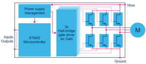 Simplified block diagram of a power inverter based on GaN transistors
Fueling the next generation of motor inverters
GaN is promising important benefits even in applications operating at low frequencies (up to 20kHz). In the realm of home appliances, motor-driven systems such as washing machines, refrigerators, air conditioners, and vacuum cleaners rely heavily on motor inverters to control speed, torque, and efficiency. Unlike industrial servo or precision motors, the physical size of these motors is largely fixed due to mechanical and functional constraints. This means that the traditional approach of reducing overall system size by shrinking the motor itself is not feasible. Instead, improvements must be sought in the inverter and power electronics that drive these motors.
In this sense, it is important to point out that the benefit of GaN over traditional silicon transistors does not come from a single parameter that stands out. It is rather the sum of different aspects concatenating together.
GaN has a de facto negligible reverse recovery charge (Qrr) and low parasitic capacitances, which in turn enable working with slightly higher dV/dt. While the motor winding and insulation limit the maximum allowable dV/dt, GaN’s capability to operate at higher switching speeds allows designers to optimise switching edges carefully.
Moreover, a safe and drastic reduction of dead-time is also achievable without risking shoot-through faults. Time between high-side and low-side switching can be easily lowered by a factor of 10. This can improve inverter efficiency and reduce switching losses without compromising motor reliability.
As remarkable as it gets, the performance is not over yet. In fact, all these “little” improvements combined lead to what may be considered the most relevant of them all: the removal of the heatsink.
Kiss your heatsink goodbye
The considerable reduction in power dissipation allows designers to reduce or even remove bulky heatsinks in the inverter power stage. The assembly line may now require fewer steps in the manufacturing process. No heatsink also means no screws or mounting joints, thus avoiding mechanical failures that can appear when the appliance is already long in the field. An interesting potential saving of service and warranty costs.
The overall result is a more compact, lightweight, and cost-effective inverter design that fits better within the demanding and highly competitive space of the home appliances market.
 700 V GaN mounted on a motor inverter running without a heatsink
The waveforms show how smooth and cold a GaN can be. In the example above, the device under test has a typical RDS(on) of 80mΩ. The motor inverter runs at a switching frequency of 16 kHz, with a maximum dV/dt slightly under 10V/ns.
A power level of about 800 W can be safely achieved without incurring thermal runaway. The increase in temperature Δt is less than 70 °C, which leaves a good margin before reaching the maximum operating junction temperature (TJmax) of 150 °C.
This remarkable result is achieved without a heatsink, with GaNs mounted on and cooled down through a common 2-layer PCB.
STPOWER GaN Transistors
STPOWER GaN Transistors are intrinsically normally off, p-GaN gate e-mode transistors that offer a zero reverse recovery charge. ST offers today seven part numbers rated 700 V breakdown voltage (VDS), with typical on-resistance RDS(on) ranging from 270 mΩ down to 53 mΩ in DPAK, PowerFLAT 8×8, and TO-LL packages.
The portfolio is rapidly growing, adding on different packages, RDS(on) and breakdown voltage levels.
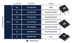
The post GaN Benefits in Motor Controls appeared first on ELE Times.
Union Minister Ashwini Vaishnaw inaugurates TI’s new, world-class R&D centre
Texas Instruments (TI) officially opened its new, state-of-the-art product research and development (R&D) centre in Bengaluru at an event commemorating the company’s 40-year presence in India. As the first multinational company to establish an R&D centre in India in 1985, TI has been instrumental in shaping India’s semiconductor landscape for four decades. The new 550,000-square-foot centre features a collaborative workspace dedicated to developing world-class chip designs. The centre includes an end-to-end reliability lab equipped with advanced testing capabilities for various environmental conditions, along with many other integrated circuit design labs.
Inaugurated by Shri Ashwini Vaishnaw, Union Minister for Railways, Information & Broadcasting, Electronics & Information Technology, Government of India, alongside TI leaders, the new centre highlights the company’s strategic vision to propel semiconductor innovation and nurture world-class design talent. This expansion reinforces TI’s commitment to developing breakthrough analogue and embedded processing technologies while strengthening its support for the design ecosystem and its growing customer base in India.
Shri Ashwini Vaishnaw, Union Minister for Railways, Information & Broadcasting; Electronics & Information Technology, Government of India, said, “I congratulate Texas Instruments on the inauguration of this world-class R&D centre in Bengaluru. TI has been a true pioneer in India’s semiconductor journey and stood as a testament to consistently nurturing the design talent ecosystem in India. The company’s expanded investment reinforces India’s position as a global hub for semiconductor design, development and supports our vision of building an innovation-led nation.”
Santhosh Kumar, president and managing director, TI India, said, “As we celebrate 40 years in India, this milestone reflects TI’s rich legacy and our strong commitment to the future. TI India’s product development and design teams drive research and breakthrough innovations for customers worldwide. Our world-class engineers are central to pioneering the next generation of semiconductor advancements.”
The company recently opened an additional sales office to strengthen its partnership with Indian customers, while the new R&D facility builds on its innovation capabilities in the region. With thousands of employees in India, TI continues to expand its presence in the region.
The post Union Minister Ashwini Vaishnaw inaugurates TI’s new, world-class R&D centre appeared first on ELE Times.
Bridging the design-to-deployment gap: How India can lead the next wave of connected device innovation
Hareesh Ramana, Chief Experience Officer, Sasken Group & President, Borqs Technologies (a Sasken Group company)
India is making significant strides in electronics manufacturing with the aim of 38% value addition within five years. The device manufacturing ecosystem has grown to a significant scale, but it still depends heavily on designs and reference architectures developed elsewhere.
Building domestic capability in electronic device design, especially IoT/connected device design, is critical to India’s ambition of becoming a major electronics manufacturing hub. India’s ambition to reach 38% value addition in electronics manufacturing will be driven not only by scaling assembly but by strengthening device design and systems engineering, which can contribute as much as 30-35% of the total value creation.
Need for in-house design capabilities:
A growing model in India’s connected-device ecosystem is design-led, end-to-end IoT product development anchored locally, covering silicon integration, embedded software, connectivity stacks, and certification. Companies like Borqs Technologies (now part of the Sasken Group) exemplify this approach, offering full-stack IoT design capabilities from within India. For OEMs, this can shorten development cycles, improve control over system integration, and reduce dependence on externally sourced IP and engineering capacity, especially in critical connectivity and compliance stages. Expanding these capabilities across the industry can help India move beyond contract manufacturing and toward the higher-value innovation layer where devices connect to data, analytics, and services.
Time to market gap:
Many IoT projects stall because hardware, firmware, cloud platforms, connectivity, and certification are handled by separate vendors with misaligned priorities.
Over the past decade, India’s product development ecosystem has matured to address these challenges, evolving from a cost-centric outsourcing base into a design-led innovation hub. Global OEMs and platform companies increasingly view India as a partner for rapid prototyping and co-innovation, not just low-cost assembly. Several end-to-end product engineering companies in India exemplify this shift by delivering integrated IoT solutions that shorten development cycles and align with global OEM roadmaps.
Integration as a strategic capability
Connected devices are no longer standalone products; they are endpoints of digital services. The differentiator is therefore systems integration across silicon, hardware, software, connectivity, and lifecycle management. A unified, end-to-end engineering model can enable:
- Faster debugging by tightening the feedback loop between hardware and software teams
- Fewer integration issues by reducing handoffs across multiple vendors
- Quicker prototyping and validation through coordinated design and test cycles
- More predictable certification and production ramp by planning compliance and manufacturability early
- A single accountable partner from concept through delivery and lifecycle management
This is particularly vital for industrial-grade devices where reliability, security, and compliance define adoption. Indian engineering firms with cross-layer capabilities are increasingly enabling platform-driven approaches that allow module reuse across verticals like automotive, energy management, and logistics.
AI and advanced technologies and product development:
Advanced technologies like AI, IoT, automation, digital twins, and cloud computing are transforming product development. AI-driven analytics reduce manual testing cycles, while digital twins simulate device behaviour under real-world conditions, enabling faster iteration and higher reliability.
Demand for software-defined vehicles, smart energy infrastructure, automated factories, and connected appliances is accelerating globally. Multinationals are expanding design centres and co-innovation programs in India to build products for both developed and emerging markets.
For India, the opportunity lies in moving beyond contract manufacturing to the high-value layer where devices meet data, analytics, and services. Mastery over sensors, edge intelligence, connectivity stacks, and lifecycle platforms can enable the country to capture a far greater share of the global electronics economy.
The coming decade will reward ecosystems that can bridge the design-to-deployment gap with reliability and speed. India has the talent, digital infrastructure, and entrepreneurial energy to lead this shift. The next step is an integrated approach that unites design, engineering, and manufacturing into a single innovation continuum.
The post Bridging the design-to-deployment gap: How India can lead the next wave of connected device innovation appeared first on ELE Times.
ST Foundation Continues Expansion of Digital Literacy Initiatives in India; Honours IFCCI ‘CSR Project of the Year’ Recognition
The ST Foundation, the non-profit corporate arm of STMicroelectronics, hosted a media briefing late January 2026 to outline its strategic expansion in India and celebrate the recent recognition of its flagship “Digital Unify” program. Dedicated to bridging the global digital divide since 2001. The Foundation’s mission has taken on critical urgency in India, where over 400 million people remain excluded from essential digital services.
Addressing the 400 Million Divide
With global data from the 2025 ITU Connectivity Report indicating that 2.2 billion people lack basic digital access, the ST Foundation has positioned India as a central focus for its “Digital Unify” (DU) initiative. The program uses a “train-the-trainer” model and local partnerships to ensure sustainable, community-owned growth.
Impact in Asia and India
In Asia alone, the foundation has 96 Digital Unify Labs, serving about 26,000 beneficiaries per year at a cost of less than $10 per student trained.
The Foundation in India was officially registered in 2018, having reached more than 180,000 trainees to date and having established over 56 Digital Unify Labs across the country.
Key Program Impact and Expansions:
- Education for Vulnerable Children: Since 2022, the “Basic Coding” program has reached over 2,500 children aged 9–13 in slum areas, providing many with their first-ever exposure to digital devices.
- Rehabilitation for Incarcerated Individuals: In partnership with the India Vision Foundation, the “Introduction to Computer Basics” (ICB) course has trained over 3,300 incarcerated people across Uttar Pradesh and Delhi (including Central Jail Rohini) to aid in their eventual reintegration into society.
- Empowering the Visually Impaired: A specialised ICB4VI pilot recently trained 17 visually impaired girls in digital skills. The Foundation is now preparing to scale this model nationwide.
Digital Unification and Cyber Concerns
The Foundation has not only been providing underprivileged people with digital literacy but has also helped them with understanding the basic risks of cyber-attacks, briefings on cybersecurity and internet safety.
Award-Winning Impact
The briefing also highlighted the Foundation’s recent accolade as the “CSR Project of the Year” at the 7th Indo-French Chamber of Commerce & Industry (IFCCI) CSR Conclave & Awards. This award recognises the program’s effectiveness in turning the digital access gap into tangible opportunities for education and employment.
By: Shreya Bansal, Sub-Editor
The post ST Foundation Continues Expansion of Digital Literacy Initiatives in India; Honours IFCCI ‘CSR Project of the Year’ Recognition appeared first on ELE Times.
R&S drives connections and innovations at MWC Barcelona 2026
Rohde & Schwarz will exhibit its extensive portfolio of next generation of wireless technologies, under the motto, “Enabling Connections, Empowering Innovations”, at the Mobile World Congress 2026 in Barcelona, Fira Gran Via, hall 5, booth 5A80 from March 2 to 5, 2026.
The path from 5G to 6G
For a seamless evolution from 5G to 6G, Rohde & Schwarz offers future-ready test solutions for mobile devices and networks. Among the many innovative solutions, the CMX500 one-box signalling tester stands out throughout multiple demos, addressing today’s and tomorrow’s testing challenges.
- Paving the way for 6G, Rohde & Schwarz showcases carrier aggregation combining FR1 and FR3 frequency ranges with its CMX500 one-box signalling tester. The demonstration validates end-to-end device behaviour across the aggregated spectrum. FR3 (7.125 to 24.25 GHz) has been identified by industry and research as a “sweet spot” for combining wide-area coverage with high capacity. Equipped with the new, upgradeable RFU18 board for the CMX500, the tester covers up to 18 GHz, giving users enough headroom for FR3 evolution and a future-ready path for testing next-generation networks.
- Another setup addresses virtual signalling testing. Based on the CMX500, Rohde & Schwarz demonstrates a new approach of shift-left testing, allowing R&D engineers to find design flaws early in their mobile radio modem chips before costly silicon fabrication. This early SDR-based validation will significantly cut time-to-market for 6G devices.
- Ray tracing simulates real-world signal propagation environments, making it a valuable technique for AI receiver testing for future 6G devices. Rohde & Schwarz will showcase the CMX500 as it creates a digital twin of signal propagation within its test environment by leveraging the VIAVI
 ray tracing engine. This enables controlled and reproducible validation of complex scenarios with high measurement precision, facilitating site-specific optimisation of radio links and reducing the need for tedious field tests.
 - Rohde & Schwarz also advances 5G and emerging 6G testing with its AI-based toolset AI Workplace for the CMX500, massively enhancing testing productivity. TechAssist uses natural language to control the CMX500, enabling rapid test-scenario setup and status/configuration queries, while an upgraded ScriptAssist with a new interface simplifies and accelerates scripting for R&D protocol and application testing as well as instrument automation. Visitors can experience these AI-powered tools in action within various setups at MWC 2026.
- Mobile XR and personal AI devices like smart glasses and wearables are key for 5G-Advanced and 6G-enabled immersive 3D communications. Delivering compelling, low-latency experiences will require rigorous, realistic testing. Rohde & Schwarz will demonstrate an end-to-end testbed centred around the CMX500, addressing AI on RAN and XR testing challenges with its ability to emulate 4G, 5G and Wi-Fi networks, applying both RF and IP impairments to reproduce real-world conditions such as interference and congestion.
- 6G ISAC (Integrated Sensing and Communication), which leverages mobile networks for object detection, is rapidly gaining traction. Rohde & Schwarz will demonstrate new capabilities of its R&S AREG800A, including the emulation of micro-Doppler signatures – in addition to distance, speed and RCS – to support object classification, such as drones.
- For testing base stations and network infrastructure, Rohde & Schwarz showcases the PVT360. It meets the requirements for testing FR1/FR2, small cells and O-RU in a single box. For the verification of frequency converting antennas used in SATCOM, NTN or 5G and 6G applications, visitors can learn about CATR-based over-the-air test chambers, enabling fast OTA-testing of phased antenna arrays.
- With the first off-the-shelf commercial mobile devices now available for 5G broadcast, Rohde & Schwarz lets visitors explore seamless rich data distribution transmission to mobile devices, innovative applications like venue casting, emergency alerts and advanced solutions for terrestrial positioning, navigation and timing.
From ground to orbit with NTN
As terrestrial and satellite-based networks converge, it becomes increasingly complex to simulate real-world conditions while meeting 3GPP requirements, for instance, when it comes to handovers within orbits, between orbits or from space to ground. As NTN technology matures alongside 5G and towards 6G, overcoming significant technical hurdles is key to realising NTN’s potential.
- Rohde & Schwarz has upgraded its CMX500 one-box signalling tester, supporting NR-NTN, NB-NTN and Direct-to-Cell (D2C/DTC) technologies in a single platform. The tester creates a digital twin of the sky, simulating orbits, bands and impairments like Doppler shifts and fading. Combined with smart features like the Constellation Insights Tool, it allows engineers to visualise satellite constellations, analyse coverage gaps and observe trajectories.
- Rohde & Schwarz also supports NTN conformance and carrier acceptance testing, offering the highest number of validated test cases for NR-NTN according to 3GPP Rel.17. In cooperation with Samsung, validations were conducted across all three test domains: RF, RRM and PCT. At MWC 2026, visitors will not only be able to experience these test cases but also see a demonstration of Viasat’s test plan for NB-NTN, covering protocol, performance and RF test scenarios.
Industry collaborations to accelerate AI-RAN
AI is becoming an integral part of the RAN, enabling performance optimisation, improved energy efficiency and more autonomous operations. As a member of the AI-RAN Alliance, Rohde & Schwarz continues industry collaboration and provides reliable test equipment for navigating interoperability in this evolving landscape.
- Rohde & Schwarz and Nokia Bell Labs have collaborated on an AI/ML-based 6G base station radio receiver employing Digital Post Distortion (DPoD) to recover distorted uplink signals. DPoD improves link budget, preserves coverage and reduces the need for dense site deployments, lowering costs. DPoD also reduces mobile device complexity and power consumption. The testbed at the Rohde & Schwarz booth, comprising the R&S SMW200A vector signal generator and the newly launched FSWX signal and spectrum analyzer will showcase the improved performance of Nokia’s AI receiver for uplink signals with different distortion levels.
- In collaboration with NVIDIA, Rohde & Schwarz will exhibit its latest proof-of-concept, also leveraging digital twin technology and high-fidelity ray tracing. This approach creates a robust framework for testing AI-enhanced base stations for both 5G-Advanced and 6G under realistic propagation conditions. This integration aims to bridge the gap between AI-driven wireless simulations and real-world deployment, facilitating more efficient and accurate testing of next-generation receiver architectures.
Next-generation Wi-Fi experience
Wi-Fi 8 sets new expectations for consistent, ultra-high-reliability and quality connectivity. Designed to handle a growing number of connected devices and demanding applications like XR or industrial IoT, IEEE 802.11bn employs ever more complex MIMO (Multiple-Input, Multiple-Output) scenarios. Rohde & Schwarz enables manufacturers with its solution portfolio, from R&D to production.
- The CMX500 one-box signalling tester is now equipped with comprehensive Wi-Fi 8 capabilities. The tester’s flexibility and embedded IP test capabilities make it a versatile solution for a broad range of Wi-Fi 8-specific tests, such as dRu (distributed resource unit), introducing distributed resource allocation, and UEQM (unequal modulation) where different MIMO layers use different modulation schemes, as well as 320 MHz channel bandwidth.
- To navigate the technical complexities of Wi-Fi 8 throughout the entire device lifecycle – from development to production – Rohde & Schwarz will exhibit the CMP180 radio communication tester, designed for testing in non-signalling mode with advanced capabilities and broad bandwidth support. The CMP180 combines two analysers and generators for efficient testing of 2×2 MIMO Wi-Fi 8 devices.
- For high-end MIMO signal generation and analysis tasks in R&D, Rohde & Schwarz will display the R&S SMW200A vector signal generator and the newly launched FSWX signal and spectrum analyser. With its outstanding standard EVM performance and in combination with its cross-correlation feature, the FSWX discovers details of Wi-Fi 8 signals that have been hidden up to now and offers new margins for optimisation. Its multichannel architecture makes the FSWX well-suited for analysing complex scenarios like multi-user MIMO (MU-MIMO).
Automotive connectivity testing
Vehicle manufacturers are integrating increasing levels of wireless connectivity to enable new user experiences, safety features and higher levels of autonomous driving. Rohde & Schwarz offers precise test solutions that cover all wireless technologies used in the automotive industry, from 5G and ultra-wideband to C-V2X and GNSS.
- With NG eCall becoming mandatory for vehicles sold in Europe starting in 2026, Rohde & Schwarz will demonstrate compliance testing capabilities using the CMX500 one-box signalling tester and R&S SMBV100B vector signal generator. The test solution also supports the upcoming Chinese automotive GNSS test standard, GB/T 45086.1 2024, expected to be mandatory for the Automotive Emergency Call System in 2027, with automated testing.
- Non-terrestrial networks have the potential to provide ubiquitous automotive connectivity and require enhancements to key components such as the chipsets, TCU and antennas. Trade show visitors can discover at MWC 2026 how the company’s comprehensive NTN test solutions can help the automotive industry create the always-connected vehicle.
Solutions for mission-critical communications and spectrum monitoring
Mission-critical communications (MCX) support public safety, first responders and emergency services by providing extremely reliable, low-latency and secure communications even in adverse conditions. Rohde & Schwarz will showcase its integrated solutions for testing devices and mobile networks, facilitating the ongoing migration to 3GPP-compliant broadband mission-critical services.
- The QualiPoc platform will be demonstrated with new capabilities for MCX testing. This smartphone-based solution allows detailed performance assessment of MCX private and group calls, including measurement of 3GPP-defined MCX KPIs. New features include direct MCX app control and the ability to measure quality of service (QoS) and quality of experience (QoE) for public safety communications. The R&S LCM, an autonomous monitoring probe, and the R&S TSMS8, the fastest network scanner, will also be on display, further expanding capabilities for both business and mission-critical networks.
- Rohde & Schwarz will also exhibit a protocol conformance test solution to verify that MCX devices and client software implementations adhere to 3GPP specifications.
- Expanding its spectrum monitoring portfolio, Rohde & Schwarz will launch two new products at MWC Barcelona 2026: These solutions will enable regulatory authorities, network operators and public services in over 100 countries to actively protect the electromagnetic spectrum and address evolving monitoring challenges. The new devices will enhance capabilities in interference hunting and regulatory compliance.
Endpoint security, network visibility and secure network solutions
Robust security solutions deliver seamless and reliable communications experiences. Rohde & Schwarz subsidiaries will also present their innovative solutions supporting the wireless ecosystem.
- The Rohde & Schwarz Networks & Cybersecurity division, comprising the subsidiaries Rohde & Schwarz Cybersecurity and LANCOM Systems, provides endpoint security, secure networks and high-quality cryptography. With products “Engineered in Germany”, they ensure trustworthy, reliable and secure data transfer, specialising in the public, critical infrastructures, defence, health, retail and SME verticals. At MWC 2026, Rohde & Schwarz Cybersecurity will showcase the Layer 2 encryptor R&S SITLine ETH NG and the R&S ComSec solution enabling secure mobile working with sensitive data on iPhones and iPads. LANCOM Systems will present an overview of its Wi-Fi 7 access point portfolio, the latest 5G router models and firewalls.
- As networks become more distributed, encrypted and dynamic, network visibility becomes indispensable. At the Rohde & Schwarz booth, visitors will experience how the ready-to-deploy, DPI-powered R&S Probe Observer delivers deep network visibility, precise real-time traffic analytics and actionable intelligence. Developed by ipoque, a Rohde & Schwarz company, this deep packet inspection (DPI) software probe analyses network traffic at the application level, enabling operators to understand, optimise, and control their networks while supporting faster detection, diagnosis and resolution of network and service issues.
Rohde & Schwarz will showcase its comprehensive portfolio of test and measurement and industry solutions at Mobile World Congress 2026 at Fira Gran Via in Barcelona, in hall 5, booth 5A80. Trade magazine editors and press representatives visiting the event are invited to schedule briefings with their press contact at Rohde & Schwarz.
The post R&S drives connections and innovations at MWC Barcelona 2026 appeared first on ELE Times.
Сторінки

