
ELE Times

Directed Energy Systems: Where Capability Ends and Control Begins
by Sukhendu Deb Roy, Industry Consultant
Key Takeaways- The economics of warfare have flipped, with cost asymmetry emerging as a primary battlefield dynamic
- Directed energy systems shift defence from inventory-driven models to energy-driven ones
- Future defence architectures will be AI-orchestrated, integrated, and multi-domain
- Semiconductor capability is central to defence sovereignty
Modern warfare is undergoing a structural and economic shift—one that is redefining how conflicts are fought and sustained. Across theatres, adversaries are increasingly deploying low-cost, high-volume threats designed not just to penetrate defences, but to exhaust them. This is not merely a tactical evolution; it is an economic strategy aimed directly at the cost structure of defence systems rather than their technical limits.
In response, Directed Energy Weapons (DEW), particularly high-energy laser (HEL) systems, are emerging as a compelling alternative. By reducing the cost per engagement to near-zero and removing dependence on finite ammunition, they signal a transition toward energy-based warfare—where power availability replaces inventory as the primary constraint.
Operational systems today, typically in the 100–300 kW class, are already capable of countering drones, small boats, and select aerial threats. However, their performance remains constrained by power density, beam quality, and thermal dissipation limits.
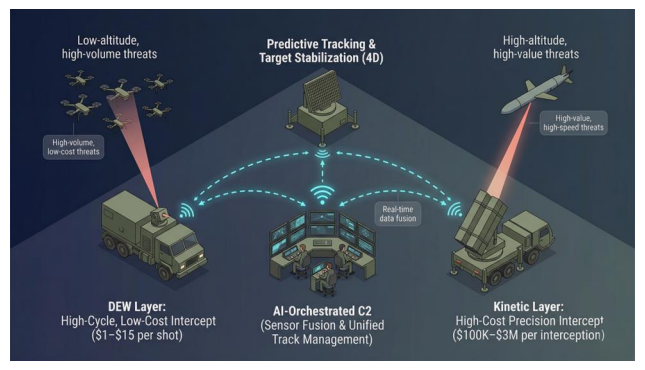
Figure 1. Emerging multi-layered defence architectures integrating kinetic and directed energy systems through AI-driven command and control.
The Problem: Capability Without ControlThis advantage, however, is not absolute. Real-world deployments continue to reveal persistent constraints—thermal limits, atmospheric attenuation, beam dwell time, and power scalability challenges. These are not isolated engineering challenges; they are systemic constraints.
More importantly, they reveal a deeper dependency: the effectiveness of directed energy systems is inseparable from the ecosystem that supports them. Performance is not defined solely by the platform, but by the electronics, semiconductors, and supply chains beneath it.
This creates a structural risk. A nation may deploy advanced directed energy systems, yet remain dependent on external control at the component and semiconductor level.
The future of defence, therefore, will not be determined by the deployment of advanced platforms alone, but by the ability to secure control over the enabling ecosystem that makes those platforms viable at scale.
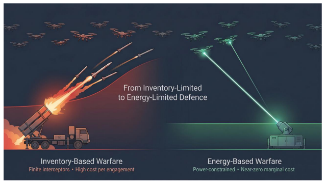
Figure 2. Directed energy systems deliver visible capability, but remain dependent on underlying electronics and semiconductor ecosystems—creating hidden vulnerabilities in control.
The Economic War of AttritionAt the heart of this transformation lies a fundamental imbalance shaping modern conflict. Defenders are increasingly forced to deploy high-value interceptors against low-cost threats, creating an unsustainable economic equation. Systems such as surface-to-air missiles or kinetic interceptors become prohibitively expensive when faced with saturation attacks.
This imbalance is not incidental—it is being deliberately operationalized through drone swarm attacks and loitering munitions designed to overwhelm defences through sheer volume rather than technological sophistication. The objective is clear: to stretch defensive resources to their limits and exploit the cost asymmetry inherent in traditional systems.
Directed energy systems fundamentally alter this equation. By shifting from consumable munitions to energy-based engagement, they dramatically reduce marginal costs and enable sustained operation without the constraints of inventory—as long as sufficient power is available.
This represents more than a technological evolution. It is a financial reset in how defence is structured and sustained. This is the defining shift from inventory-based warfare to energy-based warfare.
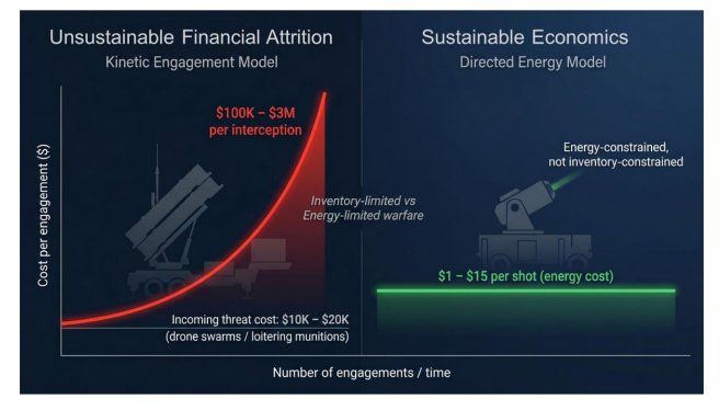
Figure 3. Cost asymmetry in modern warfare—low-cost threats forcing disproportionately expensive kinetic responses, driving unsustainable defence economics.
Without such a transition, the long-term economics of defence operations risk becoming untenable in the face of increasingly scalable, low-cost threats.
The Illusion of SovereigntyThe visible success of a directed energy intercept can be compelling. It signals speed, precision, and technological sophistication—creating the impression of true strategic independence. But that impression can be deceptive.
Beneath every such system lies a tightly integrated ecosystem of power electronics, thermal systems, optical assemblies, RF components, and semiconductors. If these critical elements are externally sourced, control has not been achieved—it has merely shifted out of view. Dependence is not eliminated; it is reconfigured.
In practice, this dependence surfaces through export controls, defence supply chain choke points, firmware constraints, and restricted access to advanced semiconductor nodes. Under normal conditions, these limitations may remain hidden. Under geopolitical stress, they translate directly into operational risk.
Capability alone does not ensure sovereignty.
Control does.
Where Control Actually ResidesTo understand where control truly resides, directed energy systems must be viewed not as standalone platforms, but as layered architectures.
At the surface lies the platform layer—the visible capability, including laser systems deployed on land, sea, or air platforms. Beneath this sits the system layer, where command-and-control frameworks, targeting systems, and sensor fusion enable coordinated operation.
Deeper still is the engineering layer, which determines real-world performance. This includes power electronics that stabilize output, thermal systems that govern endurance, and optical and beam control mechanisms that ensure precision.
At the foundation lies the control layer—the least visible, yet most decisive. This layer encompasses semiconductors, advanced materials, packaging, and the broader supply chain that sustains the system.
It is this lowest layer that anchors performance, scalability, and resilience. Any external dependence here propagates upward, constraining every layer above and limiting true autonomy.
Performance, scalability, and resilience are determined at the lowest layer. Any external dependence at the control layer propagates upward, constraining the entire system.
Sovereignty, in this context, is not a function of the platform—it is a function of control at the component and semiconductor level.
These constraints are not theoretical—they are engineered into the system itself.
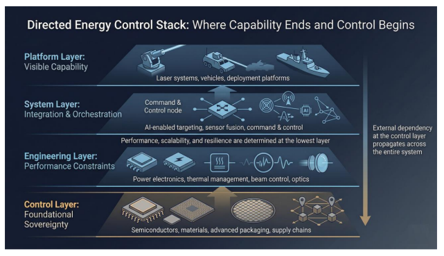
Figure 4. Directed energy performance is constrained by tightly coupled power, thermal, and semiconductor systems—highlighting the central role of control-layer technologies such as GaN-based switching.
The Real BottlenecksThe challenges facing directed energy systems are physical, not conceptual.
- Thermal constraints limit sustained firing duration
- Advanced power electronics define efficiency
- Atmospheric conditions degrade beam propagation
- Beam dwell time limits effectiveness against fast-moving targets
- AI-enabled defence systems must operate at machine speed
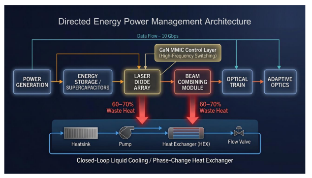
Figure 5. Directed energy constraints are interdependent—thermal, power, and control limitations must be solved as an integrated system, not in isolation.
These constraints do not exist in isolation—they reinforce and amplify one another. Addressing a single limitation, whether in thermal management or power delivery, does not translate into real operational capability on its own. What is required is coordinated industrial depth across multiple domains, from materials science and semiconductor design to power systems and real-time computation.
A directed energy system is only as effective as the ecosystem that sustains it.
From Weapons to SystemsDirected energy is no longer a standalone capability. It is steadily becoming part of integrated, AI-orchestrated defence architectures—often described as Cognitive Hybrid Defence—where multiple systems operate in coordination rather than isolation. In this emerging model, directed energy systems function alongside electronic warfare, cyber capabilities, and kinetic interceptors, all unified through real-time command-and-control frameworks.
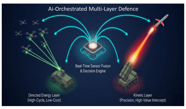
Figure 6. Transition from standalone weapons to AI-orchestrated, multi-layer defence systems, where threats are dynamically assigned to the most efficient response layer.
This shift is already visible in operational programs such as the U.S. Navy’s HELIOS system and Israel’s Iron Beam, both of which demonstrate how layered, multi-domain defence is replacing single-point solutions. The objective is no longer limited to individual interception—it is about orchestrating responses across domains with speed, precision, and economic efficiency. As this transition accelerates, control over the underlying technological ecosystem becomes even more critical.
Semiconductor Policy is Defense PolicyThis convergence carries direct implications for national strategy. Defence capability and semiconductor capability can no longer be treated as separate domains—they are structurally interdependent. Initiatives such as India’s Electronics Component Manufacturing Scheme (ECMS) and the India Semiconductor Mission (ISM 2.0) must be viewed through this lens. These initiatives are central to building semiconductor sovereignty and securing India’s position in the global defence technology supply chain. They are not merely industrial policies; they are foundational to future defence capability.
Yet the challenge is not one of intent or conceptual understanding. It lies in industrial depth—particularly in manufacturing, materials ecosystems, and advanced semiconductor fabrication. Without control over critical technologies such as Gallium Nitride (GaN)-based power electronics systems, advanced packaging, and high-reliability electronics, there is a real risk of remaining a system integrator rather than a true control holder. Sovereignty, in this context, is not achieved through system assembly but through ownership of the components and technologies that define performance and resilience.
Figure 7. Defence capability is fundamentally anchored in semiconductor ecosystems—spanning materials, manufacturing, and advanced power electronics such as GaN-based systems.
Conclusion: Capability vs ControlWhat emerges is a broader shift in how warfare itself is understood. We are moving into a phase defined by energy, integration, and system-level thinking. Directed energy systems will become increasingly visible on the battlefield, delivering immediate and measurable impact. However, the true determinants of success will remain largely invisible—embedded in defence supply chains, semiconductor ecosystems, and industrial capability.
This creates a clear strategic imperative. Nations must move beyond assembling advanced platforms to controlling them end-to-end.
Forward OutlookLooking ahead, the defining question of the next decade will not be who deploys directed energy systems first, but who can sustain and scale them under real-world conditions. Future conflicts may become power-limited rather than ammunition-limited, where grid resilience, energy density, and power electronics infrastructure and power distribution emerge as core defence parameters.
Meeting this challenge will require closer alignment between defence procurement and semiconductor strategy, sustained investment in power electronics, thermal systems, and advanced materials, and a decisive shift from platform-centric thinking to ecosystem-centric design.
Countries that recognize this transition early will build not just capability, but resilience. Those that do not will remain dependent—regardless of how advanced their visible systems may appear.
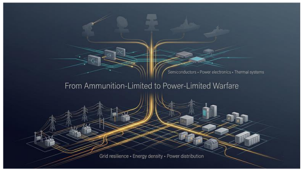
Figure 8. Future defence systems will be constrained by power, energy infrastructure, and semiconductor capability—marking the shift from ammunition-limited to energy-limited warfare.
Final PerspectiveIn the next generation of warfare, capability will be visible. Control will be decisive.
The post Directed Energy Systems: Where Capability Ends and Control Begins appeared first on ELE Times.
Boundary scan in combination with automotive applications for CAN-FD and LIN bus
Serial communication remains the backbone of electronic communication in the automotive sector. The cost-effective LIN bus with master-slave architecture and the fast multi-host fieldbus CAN-FD (Controller Area Network) have become established in this field. The great advantage and efficiency of the applications lies in the combination of both bus systems. GÖPEL electronic has now introduced an extension for the SCANFLEX Multi Port Bus I/O Module 9305 for these interfaces, which makes the functional diversity of the SCANFLEX system available for automotive interfaces in production testing.
With the new BAC module for CAN-FD/LIN, these interfaces can now be tested for functionality during production. The Bus Access Cable (BAC) is connected to one of the five slots of the SCANFLEX Multi Port Bus I/O Module 9305 and thus connected to the SCANFLEX system. This enables access to the complex test functions of the SCANFLEX boundary scan controller. The controller then takes over the simultaneous generation and dynamic distribution of the vectors and control sequences to the interfaces.
SCANFLEX is a modular JTAG/boundary scan controller. Based on state-of-the-art multi-core processors and FPGAs, it allows users to execute test and programming technologies from Embedded JTAG Solutions. Its multifunctional architecture enables these technologies to be combined flexibly and with high performance on a single platform. SCANFLEX II has eight independent, truly parallel test access ports (TAP) for up to 100MHz. This enables the synchronized execution of embedded test, debug, and programming operations via boundary scan (IEEE1149.x), processor emulation, chip integrated instruments, or the embedded diagnostics method.
About GÖPEL electronic
GÖPEL electronic develops and manufactures innovative electrical and optical test, measurement, and inspection equipment for electronic components and printed circuit board assemblies as well as industrial and automotive electronics systems. The company is active worldwide, with its own subsidiaries as well as through distributors, and generated sales of approximately 40 million euros in 2023 with 240 employees.
The post Boundary scan in combination with automotive applications for CAN-FD and LIN bus appeared first on ELE Times.
Why Every EV & 5G Phone Could Soon Be Powered by Gujarat
In a move that cements India’s transition from a consumer to a producer in the global silicon race, Prime Minister Narendra Modi officially inaugurated the Kaynes Semicon OSAT (Outsourced Semiconductor Assembly and Test) facility on March 31, 2026.
The ₹3,300 crore plant, located in the industrial heart of Sanand, marks the second major semiconductor unit to go operational in Gujarat within 900 days, following the earlier launch of the Micron facility. This rapid execution underscores the momentum of the India Semiconductor Mission (ISM) 2.0, as the country aggressively pursues a slice of the $110 billion global chip market.
A Global Export HubWhile domestic self-reliance is a key driver, the Kaynes plant is looking outward. During the ceremony, the first batch of Intelligent Power Modules (IPMs), sophisticated components that integrate 17 individual chips, was presented to Stephen Chang, CEO of Alpha & Omega Semiconductor, a California-based anchor customer.
“Today, a new bridge has been formed between Sanand and Silicon Valley,” the Prime Minister stated during his address. “The modules made here will reach American companies and, from there, power the world.”
Key Specifications of the Sanand PlantThe facility is designed for high-volume, high-precision manufacturing, focusing on sectors that are currently seeing explosive growth:
| Feature | Details |
| Investment | ₹3,300 Crore |
| Production Capacity | Approx. 6.3 Million chips per day |
| Primary Products | Intelligent Power Modules (IPMs), Multi-chip modules |
| Target Industries | Electric Vehicles (EVs), Industrial Automation, 5G Infrastructure |
| Timeline | From Cabinet approval to production in 14 months |
The inauguration is more than just a corporate milestone; it is a strategic piece of the “India Techade” vision. Unlike traditional manufacturing, the Kaynes plant focuses on the back-end of the semiconductor value chain, like assembly, testing, and packaging, which has historically been a bottleneck for Indian electronics.
Union IT Minister Ashwini Vaishnaw highlighted the speed of the project, noting that the plant moved from foundation-laying to commercial production in record time. He also pointed to the growing “Sanand-Dholera” cluster, which is being modelled after global hubs like Hsinchu in Taiwan and Gyeonggi in South Korea.
Building the Talent PipelineTo sustain this growth, Kaynes Semicon announced a memorandum of understanding with SVNIT Surat to develop a specialised workforce. This partnership aims to bridge the gap between academic theory and the rigorous standards of semiconductor cleanrooms, ensuring a steady stream of engineers for the 10 major chip projects currently approved across six Indian states.
As the ribbon was cut in Sanand, the message to the global tech community was clear: India is no longer just waiting for the future of hardware; it is assembling it.
The facility has already reported early execution success, having shipped approximately 900 multi-chip modules (IPM5) just days before the formal inauguration, signalling high operational readiness for its export commitments.
By: Shreya Bansal, Sub-Editor
The post Why Every EV & 5G Phone Could Soon Be Powered by Gujarat appeared first on ELE Times.
WSCAD ELECTRIX AI Cuts 50% Engineering Effort For Alligator Automations
Alligator Automations India Pvt. Ltd., a manufacturer of end-of-line packaging automation systems, has reduced engineering effort in electrical design by around 50% by implementing WSCAD’s E-CAD solution.
The company’s ten-person electrical engineering team now uses WSCAD for creating electrical schematics, control cabinet design, and project documentation. Previously, tasks such as wire numbering, device grouping, and bill-of-materials generation had to be performed manually, resulting in project delays and an increased risk of errors. After switching to WSCAD, many of these steps are now automated, significantly improving both efficiency and design accuracy.
“Tasks that previously required manual work are now automated,” says Sagar Bhavsar, Control Engineering Manager at Alligator Automations. “Wire numbering alone now takes roughly half the time, allowing our team to focus more on complex design and optimisation tasks.”
Alligator Automations develops customised automation solutions, including robotic palletising systems, packaging automation, automatic loading systems, and intralogistics conveyor technology. Projects cover the entire value chain – from design and development to manufacturing, installation, commissioning, and long-term support for customers in industries such as food & beverage, paint & cement, fertiliser & petrochemicals, as well as tyre and agro industries.
“Automation projects are becoming increasingly complex while engineering timelines continue to shrink,” says Dr Axel Zein, CEO of WSCAD. “At the same time, AI is fundamentally changing how electrical engineering is performed. By automating documentation, verification, and knowledge retrieval, engineers can focus more on system design and optimisation instead of repetitive tasks. The Alligator Automations example demonstrates how standardising the E-CAD environment can significantly increase engineering efficiency.”
Beyond schematic creation, WSCAD supports precise 2D and 3D control cabinet layouts, automatic wire routing, and direct data transfer to cabinet manufacturing systems. This eliminates media discontinuities and reduces sources of error. AI-supported design, documentation, and multilingual translation capabilities further accelerate project delivery while ensuring compliance and data quality.
The post WSCAD ELECTRIX AI Cuts 50% Engineering Effort For Alligator Automations appeared first on ELE Times.
Vishay Intertechnology Automotive Grade Photovoltaic MOSFET Driver Boosts Reliability and Lowers Costs in High Voltage Systems
Vishay Intertechnology has introduced a new Automotive Grade photovoltaic MOSFET driver that is the first such device in the compact SMD-4 package to provide a creepage distance of 8 mm and mould compound with a comparative tracking index (CTI) of 600. Designed to increase safety and reliability in high voltage automotive applications — while simplifying designs and reducing costs — the Vishay Semiconductors VODA1275 features the industry’s fastest turn-on times and the highest open circuit voltage and short circuit current in its class.
Classified as providing reinforced isolation, the device delivers an open circuit voltage of 20 V typical, short circuit current of 20 μA, and turn-on time of 80 μs, which is three times faster than competing devices. These characteristics enable quicker and more reliable driving of MOSFETs and IGBTs in high-voltage systems. In addition, the device’s working isolation voltage of 1260 Vpeak and isolation test voltage of 5300 VRMS make it ideal for 800 V+ battery systems.
AEC-Q102 qualified, the VODA1275 is intended for use in pre-charge circuits, wall chargers, and battery management systems (BMS) for electric (EV) and hybrid electric (HEV) vehicles. While designers previously had to use two MOSFET drivers in series to generate the higher voltages required in these applications, the device’s high open-circuit output voltage allows them to use just one, saving space and lowering costs. In addition, the driver enables the creation of custom solid-state relays to replace legacy electromechanical relays in next-generation vehicles.
The optically isolated VODA1275 draws all the current required to drive its internal circuitry from an infrared emitter on the low-voltage side of the isolation barrier. This construction simplifies designs and lowers costs by eliminating the need for an external power supply. The MOSFET driver is RoHS-compliant, halogen-free, and Vishay Green.
The post Vishay Intertechnology Automotive Grade Photovoltaic MOSFET Driver Boosts Reliability and Lowers Costs in High Voltage Systems appeared first on ELE Times.
ROHM has added New Lineup of 17 High-Performance Op Amps Enhancing Design Flexibility
ROHM has added the new CMOS Operational Amplifier (op amp) series “TLRx728” and “BD728x” to its lineup. These are suitable for a wide range of applications, including automotive, industrial, and consumer systems. A broad lineup also makes product selection easier.
In recent years, demand for high-accuracy op amps has been rapidly increasing as automotive and industrial systems become more sophisticated, demanding faster speed, better precision, and higher efficiency. In applications requiring amplification of sensor outputs, minimising signal error and delay is essential. To meet these requirements, a well-balanced set of key characteristics is needed, including Input Offset Voltage, Noise, and Slew Rate.
These new products are high-performance op amps that offer a low input offset voltage, low noise, and high slew rate. TLRx728 features an input offset voltage of 150 μV (typ.), while the BD728x offers 1.6 mV (typ.). Both series have a noise voltage density of 12 nV/√Hz at 1kHz and a slew rate of 10 V/μs. They are therefore suitable for a wide range of precision applications, including sensor signal processing, current detection circuits, motor driver control, and power supply monitoring systems. Both series are designed to balance versatility and high performance rather than being limited to specific applications.
Application Examples
Automotive equipment, industrial equipment, and consumer electronics.
Example use case: Sensor signal processing, current detection circuits, motor driver control, and power supply monitoring systems.
The post ROHM has added New Lineup of 17 High-Performance Op Amps Enhancing Design Flexibility appeared first on ELE Times.
Govt Infuses ₹258 Crore Into 128 Startups to Drive DeepTech and IP Creation
In a major move to solidify India’s standing as a global high-tech hardware hub, the Union Government has announced a strategic investment of ₹257.77 crore (approximately $31 million) into 128 technology startups.
The announcement, shared by Minister of State for Electronics and IT, Jitin Prasada, in a written reply to the Rajya Sabha on Friday, March 27, 2026, highlights a shift toward “risk capital” for sectors critical to national security and economic self-reliance.
The “Fund of Funds” MechanismThe investment was executed through the Electronics Development Fund (EDF), which operates under a “Fund of Funds” model. Instead of direct equity, the EDF acts as an anchor investor in eight professionally managed “Daughter Funds” (early-stage venture and angel funds).
These Daughter Funds have leveraged the government’s initial contribution to mobilise a total of ₹1,335.77 crore in follow-on investments for startups specialising in:
-
Semiconductor Design & Nano-electronics
-
Cybersecurity & AI/ML
-
Robotics & IoT
-
Medical Electronics (HealthTech)
As of late February 2026, the ripple effect of this capital injection has already yielded significant socio-economic returns:
-
Job Creation: Over 22,700 high-skilled jobs have been generated within the supported startups.
-
Intellectual Property: The companies have successfully filed or acquired more than 300 IPs, reinforcing India’s domestic design capabilities.
-
Profitable Exits: The government has already realised ₹173.88 crore from 37 successful exits, proving that DeepTech ventures are becoming increasingly viable for investors.
While the government aims for pan-India growth, the current investment data shows a strong concentration in existing tech corridors. Bangalore remains the undisputed leader, housing 88 of the 128 funded startups.
A Strategic Pivot Toward Self-RelianceThis news comes on the heels of the Ministry of Electronics and IT (MeitY) approving 29 additional projects under the Electronics Component Manufacturing Scheme, involving a cumulative investment of ₹7,104 crore.
By focusing on the “Daughter Fund” model, the government ensures that capital is managed by industry experts while maintaining a minority stake—a move designed to encourage private venture capital to take more “brave” bets on hardware and indigenous R&D rather than just consumer-facing software apps.
“The goal is to build a self-sustaining electronics ecosystem,” stated the Ministry. “We aren’t just looking for the next ‘unicorn’; we are looking for the next breakthrough in Indian-owned IP.”
By: Shreya Bansal, Sub-Editor
The post Govt Infuses ₹258 Crore Into 128 Startups to Drive DeepTech and IP Creation appeared first on ELE Times.
Nuvoton Launches Upgraded Driving Smart Device, NuMicro M3331 Series MCU
As the global transition toward industrial automation and smart living accelerates, the security and processing efficiency of microcontrollers (MCUs) have become decisive factors for enterprises’ success in the business-to-business market. Nuvoton Technology has announced the launch of its new NuMicro M3331 series 32-bit microcontroller. Powered by the Arm Cortex-M33 core, the M3331 series delivers exceptional performance at operating frequencies of up to 180 MHz and integrates TrustZone technology, providing a robust hardware foundation for industrial control, smart factories, smart buildings, and renewable energy.
The M3331 series is more than just a hardware platform; it is an integrated solution designed to address the challenges customers face when processing complex control algorithms and protecting intellectual property (IP). Featuring the Cortex-M33 core with built-in DSP instruction set and a single-precision floating point unit (FPU), it runs up to 180 MHz. The M3331 series is built with comprehensive security mechanisms. Through hardware-level Secure Boot, it ensures that the system executes only certified and authorised firmware from startup, establishing an immutable root of trust. To protect core IP assets, it features eXecute-Only-Memory (XOM) to safeguard core algorithms and eliminate the risk of code leakage. Additionally, the TrustZone technology partitions a secure execution environment to effectively defend against malicious attacks.
Designed for reliability, the M3331 series supports a wide operating temperature range from -40°C to +105°C and exhibits superior interference resistance (ESD HBM 4 kV / EFT 4.4 kV), significantly reducing the risk of downtime caused by environmental factors. To further enhance system reliability, the 512 KB Flash memory supports Error Correction Code (ECC) for detecting and repairing bit-flip errors. Furthermore, within the 320 KB SRAM, a hardware parity check is provided for the 64 KB core area, achieving true industrial-grade system resilience.
To meet the diverse communication demands of the IoT era, the M3331 series introduces an I3C interface and two CAN FD controllers, greatly increasing data throughput between sensors and control nodes. For high-speed peripherals and mass storage, it includes a built-in USB 2.0 High-Speed OTG controller (with on-chip PHY) and an SDH (Secure Digital Host Controller) interface, delivering exceptional performance for both gaming products requiring low-latency transmission and smart consumer devices needing high-bandwidth storage.
Moreover, the M3331 series features a 12-bit ADC with a sampling rate of up to 4.2 Msps, accurately capturing subtle changes in analogue signals. With up to 48 PWM outputs, it provides precise control solutions for professional photography lighting and stage lighting. Specifically, the series is equipped with ELLSI (Enhanced LED Light Strip Interface) and up to 10 LLSI (LED Light Strip Interface) interfaces, supporting next-generation gaming ARGB LED control protocols. This offloads the CPU and reduces development difficulty, enabling brilliant and fluid dynamic LED effects. The M3331 series offers a variety of package options, from the compact QFN 33 (4×4 mm) to the high-pin-count LQFP 128 (14×14 mm), helping customers optimise their PCB layouts.
To accelerate time-to-market, Nuvoton provides NuMaker-M3333KI and NuMaker-M3334KI evaluation boards, along with full support for mainstream RTOS (FreeRTOS, Zephyr, RT-Thread) and GUI libraries (emWin, LVGL). This ecosystem empowers customers to build stable system solutions rapidly.
The M3331 series consists of two subseries: the M3333 series (without USB 2.0 support) and the M3334 series (with USB 2.0 support).
The post Nuvoton Launches Upgraded Driving Smart Device, NuMicro M3331 Series MCU appeared first on ELE Times.
India Boosts Tech Manufacturing: Government Approves 29 New Electronics Component Projects Worth ₹7,100 Crore
In a significant move to fortify India’s position as a global electronics hub, the Ministry of Electronics and IT (Meity) has approved 29 new applications under its flagship component manufacturing scheme.
The announcement, made on Monday by IT Secretary S. Krishnan, marks a substantial expansion of the nation’s industrial capacity. The newly sanctioned projects represent a cumulative investment of ₹7,104 crore, signalling robust private sector confidence in the government’s “Make in India” initiatives.
Economic Impact and Job CreationThe scale of the approved projects is expected to ripple through the domestic economy. According to Secretary Krishnan, the fresh wave of investment is projected to:
-
Generate 14,246 new jobs directly within the electronics manufacturing segment.
-
Yield a production value of ₹84,515 crore, significantly reducing reliance on imported sub-assemblies and parts.
This latest round of approvals brings the total number of sanctioned projects under the Meity scheme to 75. By focusing specifically on components—the building blocks of smartphones, computers, and automotive electronics—the government aims to move beyond simple assembly and build a more resilient, end-to-end domestic ecosystem.
“The approval of these 29 applications underscores our commitment to deepening the electronics value chain in India,” a senior official noted, highlighting that the move is a strategic step toward the country’s goal of reaching a $300 billion electronics production target by 2026.
The scheme continues to be a cornerstone of India’s strategy to compete with regional manufacturing giants, providing the necessary fiscal support to offset the high costs of setting up sophisticated component units.
The post India Boosts Tech Manufacturing: Government Approves 29 New Electronics Component Projects Worth ₹7,100 Crore appeared first on ELE Times.
STMicroelectronics expands 800 VDC AI datacenter power conversion portfolio with new 12V and 6V architectures in collaboration with NVIDIA
STMicroelectronics has announced the expansion of its 800 VDC power conversion portfolio with two new advanced architectures: 800 VDC to 12V and 800 VDC to 6V. Developed according to the NVIDIA 800 VDC reference design, these new power conversion stages complement the previously introduced 800 VDC to 50V solution. The rapidly emerging 800 VDC data centre architecture enables higher energy efficiency, reduces power losses, and supports more scalable, high compute density infrastructure for hyperscalers and AI compute.
“As AI infrastructure compute scale continues to expand fast, it requires higher voltage distribution and greater density, which can only be achieved with system-level innovation for each of the different AI server form factors,” said Marco Cassis, President, Analog, Power & Discrete, MEMS and Sensors Group Head of STMicroelectronics’ Strategy, System Research and Applications, Innovation Office at STMicroelectronics. “With these new converters for 800 VDC power distribution, ST brings a complete set of solutions to support the deployment of gigawatt-scale compute infrastructure with more efficient, scalable, and sustainable power architectures.”
A complete 800 VDC ecosystem for the different AI server form factors
The expansion to 12V and 6V output stages reflects the industry move toward different server architectures requiring different power delivery topologies depending on GPU generation, server height, form factor, and thermal envelope for large-scale training clusters, inference farms, and high-density AI infrastructures. The 50V, 12V, and 6V intermediate DC buses will all coexist in AI data centres depending on rack density, GPU configuration, and cooling strategy.
The new 800 VDC to 12V converter enables high-efficiency distribution from rack-level power shelves directly to the voltage domains that feed advanced AI accelerators.
The new 800 VDC to 6V path allows OEMs to reduce the number of conversion stages and move the 6V bus closer to the GPU. This reduces copper usage, minimises resistive losses, and improves transient performance, a critical differentiator for large-scale training clusters.
Back in October 2025, STMicroelectronics introduced a fully integrated prototype power‑delivery system showcasing a compact GaN‑based LLC converter operating directly from 800 V at 1 MHz with over 98% efficiency and exceptional power density in a smartphone‑sized footprint exceeding 2,600 W/in³ at 50 V.
The three solutions combine ST technologies across power semiconductors (silicon, SiC, GaN), analogue and mixed-signal, and microcontrollers.
Technical highlights of the new 12V and 6V architectures
Direct 800 VDC to 12V high-efficiency conversion:
- Eliminates the traditional 54V intermediate stage, reducing conversion steps and system-level losses.
- Enables higher rack-level efficiency, lower copper usage, and simplified integration for future GPU generations.
- Includes a newly developed high-density power delivery board (PDB) achieving efficiency targets exceeding the sum of the previous two-stage conversion paths.
800 VDC to 6V architecture for GPU-nearing conversion:
- Is designed for system builders who require power stages closer to the GPU, minimising IR drop and improving response under fast load transients.
- Completes the topology portfolio for servers with ultra-dense GPU configurations.
The post STMicroelectronics expands 800 VDC AI datacenter power conversion portfolio with new 12V and 6V architectures in collaboration with NVIDIA appeared first on ELE Times.
Geopolitical Shifts in West Asia: India Tracks Impact on Vital Shipping & Logistics Corridors
In a written reply, Minister of State for Commerce & Industry, Jitin Prasada, informed the Rajya Sabha that incentives worth Rs. 15,554 crores have been provided under the large-scale electronics manufacturing & IT hardware 2.0 schemes. Additionally, a sum of Rs. 2,377.56 crore has been disbursed under the automobiles & auto components sector.
Prasad further highlighted that the PLI schemes have attracted investments worth more than Rs. 2.16 lakh crore so far. Until now, the government has rolled out the PLI scheme for 14 sectors with the aim of strengthening domestic manufacturing and boosting exports.
Providing a sectoral breakdown of funding, the minister informed that Rs 6,022 crore has been disbursed for the pharmaceutical sector, Rs 1,859 crore for telecommunications, and Rs 2,163 crore for food products. Other allocations include Rs 55 crore for bulk drugs, Rs 157 crore for medical devices, Rs 281 crore for white goods, Rs 93 crore for drones, Rs 81 crore for IT hardware, Rs 55 crore for textiles, and Rs 132 crore for speciality steel.
No incentives have been disbursed so far for high-efficiency solar PV modules and advanced chemistry cell (ACC) battery schemes, he added.
Commenting on the dynamics of West Asia and the Gulf countries, the minister highlighted their importance as key markets for Indian agricultural exports. The region, including UAE, Saudi Arabia, Oman, Kuwait, Qatar, Bahrain, as well as Iran, Iraq and Yemen, accounted for exports worth USD 10.68 billion in 2024-25, nearly 20.5 per cent of India’s total agri exports.
These exports span a wide range of products, including cereals, animal products, fruits and vegetables, spices and processed foods sourced from across the country.
Prasada said the government is closely monitoring the evolving geopolitical situation in West Asia and its impact on trade, shipping routes and logistics. Exporters have reported challenges such as higher freight rates, war-risk surcharges, container shortages, shipment delays and port congestion.
By: Shreya Bansal, Sub-Editor
The post Geopolitical Shifts in West Asia: India Tracks Impact on Vital Shipping & Logistics Corridors appeared first on ELE Times.
63SATS Cybertech Reaffirms Strategic Partnership with CyberSec India Expo 2026 to Advance India’s Cyber Defence Ecosystem
Amid growing cybersecurity risks in the industry, 63SATS Cybertech has renewed its strategic title partnership with CyberSec India Expo 2026 for the second consecutive year, strengthening efforts to advance India’s rapidly evolving cybersecurity ecosystem.
The expo, scheduled for April 23–24, 2026, at the Bombay Exhibition Centre, Mumbai, will bring together CISOs, CIOs, CTOs, DPOs, policymakers, security leaders, enterprise decision-makers, and technology providers to examine emerging risks, regulatory developments, and advanced defence strategies shaping the digital economy.
As organisations navigate increasing exposure to sophisticated cyber threats and stricter compliance requirements, the platform is expected to facilitate focused discussions on securing critical infrastructure, digital public systems, and enterprise environments. It will also serve as a meeting ground for solution providers and end users to exchange practical insights and explore scalable security frameworks.
Through this renewed association, 63SATS will contribute its expertise across security operations, threat intelligence, and risk mitigation, while engaging with industry stakeholders on addressing current and emerging cybersecurity challenges.
Mr Taher Patrawala, Managing Director, Media Fusion, said, “As digital adoption accelerates across sectors, with India’s digital economy projected to reach $1 trillion by 2030 and over 900 million internet users driving unprecedented data exchange, cybersecurity is becoming central to sustaining trust and business continuity. Our continued engagement with 63SATS strengthens the platform’s ability to bring together expertise, real-world perspectives, and solution-driven discussions that are critical to navigating today’s increasingly complex threat landscape.”
Mr Neehar Pathare, Managing Director, CEO & CIO, 63SATS Cybertech added, “As India advances into a new era of digital governance with the rollout of the Digital Personal Data Protection framework, organisations are being held to significantly higher standards of accountability and compliance. In this environment, cybersecurity is no longer just a technical function but a critical pillar of risk management and business resilience. Our continued partnership with CyberSec India Expo reflects our commitment to driving industry-wide alignment with evolving regulatory mandates, while fostering meaningful conversations around building secure, compliant, and future-ready digital ecosystems.”
With increasing regulatory oversight, growing digital adoption, and heightened exposure to cyber risks, the partnership signals a broader industry shift toward integrated, ecosystem-led approaches to cybersecurity. CyberSec India Expo 2026 is positioned to serve as a critical convergence point for aligning strategy, technology, and policy in response to these challenges.
The post 63SATS Cybertech Reaffirms Strategic Partnership with CyberSec India Expo 2026 to Advance India’s Cyber Defence Ecosystem appeared first on ELE Times.
Nuvoton and Trustonic Collaborate to Strengthen Security of NuMicro MA35 Series MPU
Leading semiconductor manufacturer, Nuvoton, has partnered with pioneering cybersecurity business, Trustonic, to strengthen the capability of its advanced NuMicro® MA35 series MPU.
Established in 2008, Nuvoton was founded to bring innovative semiconductors to market and has since evolved into a leading name in the provision of microcontroller application integrated circuits (ICs), audio application ICs and cloud & computing ICs.
To strengthen the security of the solution, the Trusted Secure Island (TSI) of Nuvoton’s NuMicro MA35 series integrates Trustonic’s Trusted Execution Environment (TEE), Kinibi.
Having obtained the World’s first comprehensive EAL5+ certification in 2022, ‘Kinibi’ is now deployed to nearly 3 billion smart devices and 20 million vehicles globally, with zero safety violations. Its integration in the NuMicro MA35 series creates a secure environment that drives Protection, Detection, and Recovery for IoT products, including EV chargers.
Walter Tseng, Vice President of the Microcontroller Business Group at Nuvoton, explained: “Our partnership with Trustonic represents a significant milestone in Nuvoton’s commitment to providing industry-leading security for the industrial IoT market. By integrating the EAL5+ certified Kinibi TEE into our NuMicro MA35 series, we are providing our customers with a robust, hardware-backed security foundation. This collaboration ensures that critical industrial applications—from edge gateways to smart factory automation—are protected against evolving cyber threats through a dedicated ‘Protection, Detection, and Recovery’ framework, all while maintaining the high performance our users expect.”
Andrew Till, General Manager of Secure Platform for Trustonic, added: “Nuvoton’s MA35 platform is designed for high-performance edge applications, and security is critical to its success. Integrating Kinibi provides a proven Trusted Execution Environment that protects sensitive operations and enables manufacturers to build secure, scalable industrial IoT solutions with confidence.”
The post Nuvoton and Trustonic Collaborate to Strengthen Security of NuMicro MA35 Series MPU appeared first on ELE Times.
STMicroelectronics and Leopard Imaging use NVIDIA Jetson-ready multi-sensor module for robotics vision
STMicroelectronics and Leopard Imaging have introduced an all-in-one multimodal vision module for humanoid and other advanced robotics systems. Combining ST imaging, 3D scene-mapping, and motion sensing with the NVIDIA Holoscan Sensor Bridge technology, the module integrates natively with NVIDIA Jetson and NVIDIA Isaac open robot development platform, simplifying and accelerating vision system design within the size, weight, and power constraints of humanoid robots.
“Humanoid robotics is moving beyond research projects and demonstrations to deliver powerful new machines for a wide range of roles in manufacturing and automotive factories, logistics and warehousing, as well as retail and customer service,” said Marco Angelici, Vice-President of Marketing and Application for Analogue Power MEMS and Sensors, at STMicroelectronics. “Our collaboration with Leopard Imaging brings market-leading ST sensors and actuators, seamlessly integrated into the NVIDIA robotics ecosystem, to accelerate the deployment of physical AI applications with human-like awareness.”
“Accessing ST sensors and actuators directly within the ecosystem has allowed us to standardise and streamline data acquisition and logging for humanoid robot vision across the HSB interface,” said Bill Pu, CEO of Leopard Imaging. “Robot builders can use our multi-sensing vision module with Isaac tools to accelerate learning and quickly bridge the ‘sim-to-real’ gap.”
Powered by the NVIDIA Holoscan Sensor Bridge, the new module integrates seamlessly with NVIDIA Jetson over Ethernet for real-time sensor data ingestion and NVIDIA Isaac open robot development platform, which offers open AI models, simulation frameworks and libraries for developers. The new module includes a build system and application programming interfaces (APIs), artificial intelligence (AI) algorithms curated for mobile robots, sample applications, domain randomisation, and a simulation environment containing sensor models.
ST continues to integrate its sensors, drivers, actuators, controllers, and development tools into the NVIDIA robotics ecosystem as a key NVIDIA robotics and edge AI partner, including high-fidelity models and proof-of-concept modules.
Technical information
The Leopard Imaging Systems vision module incorporates:
For vision-based sensing, the ST VB1940 automotive-grade RGB-IR 5.1-megapixel image sensor has combined rolling shutter and global shutter modes. ST has also released a mass market and industrial version V**943, part of the ST BrightSense product family, existing in monochrome or RGB-IR, in die or packaged sensor.
For motion sensing, the LSM6DSV16X 6-axis inertial measurement unit (IMU) embeds ST machine-learning core (MLC) for AI in the edge, sensor-fusion low-power (SFLP), and Qvar electrostatic sensing for user-interface detection.
For 3D depth sensing, the VL53L9CX dToF all-in-one LiDAR module, part of the ST FlightSense product family, provides 3D depth sensing with accurate ranging up to 9 meters. With its resolution of 54 x 42 zones (nearly 2,300 zones) combined with a wide 55°x42° FoV providing 1° angular resolution, short and long-distance measurements and small objects detection are achievable at up to 100 fps.
The post STMicroelectronics and Leopard Imaging use NVIDIA Jetson-ready multi-sensor module for robotics vision appeared first on ELE Times.
Decoding SDV Revolution: Sensors, AI, and the Future of Automotive Architecture
At Auto EV TVS Summit, 2025, a panel of industry leaders—from semiconductor companies to automotive software firms—gathered to discuss one of the most transformative shifts underway in mobility: the rise of the Software-Defined Vehicles (SDVs). Moderated by Mohammed Saeed Mombasawala, CTO at Keysight Technologies, the discussion brought together voices from Bosch Global Software Technologies, Marelli India, NXP Semiconductors, Aumovio, and Auto Ascent to unpack how vehicles are evolving from mechanical machines into continuously upgradeable software platforms.
The consensus across the panel was clear: software is no longer an auxiliary component in the automotive stack—it is becoming the primary architecture around which the vehicle is built.
The Shift Toward “Intelligence on Wheels”Software-defined vehicles represent a departure from the traditional automotive model, where functionality was fixed at the time of manufacturing. Instead, SDVs rely on software layers that can evolve through updates, new services, and data-driven improvements throughout a vehicle’s lifecycle. “SDV is essentially about delivering affordable intelligence on wheels,” explained Bosch’s Naved Narayan during the panel discussion.
The concept is already beginning to take shape in India. Features such as over-the-air updates, connected vehicle services, and Level-2 driver assistance systems are gradually entering the market. However, unlike Western markets where premium vehicles dominate adoption, India’s automotive ecosystem operates under a different constraint: cost sensitivity.
Industry participants emphasized that the success of SDVs in India will depend on achieving a delicate balance between technological sophistication and affordability.
India’s SDV Journey: Progress, But With ConstraintsWhile the SDV revolution is global, India’s pathway has unique challenges. Panelists noted that the country is progressing toward connected and intelligent mobility, but several structural barriers remain.
Latha Chembrakalam, Founder and CEO of Auto Ascent, highlighted that the industry is driven by three key factors: safety, ease of use, and joy of driving. Software-defined architectures promise to enhance all three—but India must simultaneously contend with infrastructure gaps and regulatory limitations.
“India is a cost-sensitive market, and infrastructure readiness also plays a major role,” she noted. “While progress is visible, technological capabilities and regulatory frameworks still need to evolve to fully support SDV adoption.” Yet there are encouraging signs. Automakers such as Mahindra and MG have already begun introducing advanced connected features and driver assistance technologies in the Indian market, creating early momentum.
The New Architecture of the VehicleAt the engineering level, SDVs are forcing a fundamental redesign of vehicle electronics. Traditional vehicles rely on dozens of electronic control units (ECUs), each responsible for a specific function. SDVs, however, are shifting toward centralized computing architectures, where domain controllers or zonal controllers manage multiple vehicle functions.
This transformation also introduces new challenges. Automotive companies must reconcile modern SDV architectures with legacy platforms and existing software stacks. “For new electric vehicle platforms, it is easier to design from scratch,” Chembrakalam explained. “But the real complexity lies in integrating SDV capabilities into existing vehicle platforms with legacy systems.”
In addition, the industry still lacks fully standardized architectures across OEMs, Tier-1 suppliers, and technology vendors. Without stronger coordination, experts warned, the ecosystem risks becoming fragmented.
Sensors, Connectivity, and the Edge Computing Challenge
Software-defined vehicles depend heavily on three technological pillars:
- Sensors
- Connectivity
- In-vehicle compute
Radar, cameras, LiDAR, and other sensing technologies collectively form the vehicle’s perception system. Rather than relying on a single sensor type, most companies now favor sensor fusion architectures that combine multiple sensing modalities. Rajkumar Anantharaman of NXP noted that radar remains one of the most critical sensing technologies due to its reliability across weather conditions. However, cameras provide complementary information, such as object classification and visual context.
“Radar alone cannot solve everything,” he said. “The industry is moving toward fusion architectures where radar and camera data are combined to improve environmental perception.” At the same time, sensing systems are also becoming increasingly intelligent. Modern radar chips now integrate edge processing capabilities, allowing them to detect and classify objects directly on the sensor rather than transmitting raw data to a central processor.
This shift toward edge AI processing helps reduce latency and bandwidth requirements.
Connectivity: Why Latency MattersConnectivity plays another crucial role in the SDV ecosystem. While current vehicle platforms rely primarily on 4G networks, panelists believe 5G—and eventually 6G—will enable new levels of vehicle intelligence, particularly for vehicle-to-vehicle (V2V) and vehicle-to-infrastructure (V2X) communication.
The reason is latency. Even a delay of a few hundred milliseconds can significantly affect vehicle safety systems. In collision scenarios, a 200-millisecond delay could translate into several meters of additional braking distance. Future networks promise to reduce latency to just a few milliseconds, enabling faster information exchange between vehicles and surrounding infrastructure.
However, experts cautioned that India’s current telecommunications infrastructure still needs to mature before such capabilities can be widely deployed.
AI, Data, and the Digital Twin RevolutionPerhaps the most complex dimension of SDVs lies in software development itself. Unlike traditional automotive software, SDV platforms require continuous integration, machine learning models, and large-scale data pipelines.
Training autonomous and driver-assistance systems requires massive datasets capturing real-world driving conditions. Yet India presents a unique challenge in this area: driving environments that are far less structured than those in Western markets. Unpredictable traffic behavior, unmarked roads, and unusual scenarios—from animals crossing highways to dense urban congestion—make it difficult to collect sufficient real-world training data.
To overcome this limitation, companies are increasingly relying on digital twins, simulation environments, and synthetic data generation. These virtual environments allow engineers to simulate thousands of driving scenarios before deploying software in actual vehicles. By shifting validation earlier in the development process—known as “shift-left engineering”—companies can test and refine software models without relying entirely on expensive physical vehicle testing.
Vehicles That Improve Over TimeOne of the most intriguing aspects of SDVs is the possibility that vehicles may increase in value over time. Traditionally, a car’s capabilities remained fixed after leaving the factory. With SDVs, however, software updates can introduce entirely new features years after purchase.
Bosch’s Narayan described this shift as “an upgrade without actually upgrading the vehicle.” Through over-the-air updates, automakers can introduce new driver assistance features, improved algorithms, or additional digital services long after the vehicle has been sold.
At the same time, consumer expectations are rapidly evolving. According to Yogesh Davangere Adevappa, rising awareness of global technology trends—driven by social media and digital exposure—is pushing buyers to expect more intelligent and feature-rich vehicles. “People are increasingly aware of the technologies available worldwide,” he noted during the panel discussion. “That awareness is driving demand for vehicles with more connected features, safety systems, and intelligent capabilities.”
Why the Software-Defined Vehicle MattersUltimately, the SDV transformation is about more than just technology. It represents a fundamental redefinition of what a vehicle is. For consumers, the appeal lies in enhanced safety, convenience, and personalized driving experiences. For automakers, SDVs open the door to entirely new business models built around software services and continuous updates.
There is also growing demand for customization in vehicles. Vikram Bhatt, Aumovio, pointed out that SDV architectures allow drivers to configure vehicle behavior dynamically—whether enabling features like park-assist modes, obstacle detection systems, or personalized driving configurations. These runtime adjustments represent a fundamental shift from static vehicle functions to software-enabled experiences.
Yet despite this progress, panelists acknowledged that India is still at an early stage of SDV deployment compared to global markets.
As one panelist summarized during the discussion, the future of mobility may not just be electric or autonomous—it will be software-driven at its core.
The post Decoding SDV Revolution: Sensors, AI, and the Future of Automotive Architecture appeared first on ELE Times.
Graphene in Focus: How Nanotechnology is Transforming Electronics?
As miniaturisation and increasingly complex design architectures continue to define modern technology, nanotechnology is emerging as a frontier discipline shaping the trajectory of innovation—from medical and electronic devices to energy infrastructure and beyond. Simply stated, as the focus of electronics development shifts towards the engineering and application of materials at the atomic and molecular scale—typically between 1 and 100 nanometres—certain physical, chemical, and electrical limitations begin to surface. When conventional materials such as silicon and copper are miniaturised to the nanoscale, they often encounter issues such as increased resistance, heat generation, and reduced performance. To address these limitations, Graphene, an sp²-hybridized two-dimensional honeycomb lattice, has emerged as one of the most promising materials for next-generation electronic systems.
Amid rapid advances across the nanotechnology landscape, graphene is increasingly regarded as a flagship material in nanoscale engineering, attracting significant attention, particularly in electronics.
While Graphene continues to attract significant research interest due to its exceptional properties, the transition from laboratory-scale breakthroughs to commercially viable semiconductor technologies remains a complex challenge. Industry players such as Weebit Nano emphasise that beyond material performance, factors such as manufacturability, process compatibility, and scalability are equally critical. This creates a dynamic balance in nanoelectronics—between exploring high-potential emerging materials and developing solutions that can be seamlessly integrated into existing semiconductor fabrication ecosystems.
Owing to its exceptional electrical conductivity and extremely high electron mobility, graphene is being explored for a wide range of electronic components, including high-speed transistors, flexible circuits, and highly sensitive biosensors. The material is both electrically and thermally efficient, enabling electronic devices to operate with improved performance while generating less heat. These properties have positioned graphene as a promising complement—and in some cases a potential alternative—to conventional materials such as silicon in applications including touchscreens, sensors, and next-generation electronic interfaces.
When nanotechnology converges with electronics, the field is commonly referred to as Nanoelectronics. Nanoelectronic systems require extremely high switching speeds and efficient charge transport while minimizing heat buildup in densely packed circuits. In this context, Graphene offers exceptional carrier mobility—reaching approximately 100,000 cm²/V·s under ideal conditions—making it an attractive material for high-frequency electronic applications. Additionally, as electronic components become increasingly dense in nanoelectronic architectures, thermal management becomes a critical challenge. Graphene’s remarkably high thermal conductivity enables efficient heat dissipation, thereby helping maintain the reliability and performance of nanoscale electronic systems.
Let’s look into some applications of Graphene in nanoelectronics:
Graphene Field-Effect Transistors (GFETs)
Graphene Field Effect Transistors are advanced, ultra-sensitive electronic components comprising a channel made of a single-atom-thick layer of graphene, enabling modulation of current by an electric field.
Structure: A GFET typically consists of three things: Source, drain & a gate (top or back).
- Channel: The space between the Source & the Drain makes up a channel where a 2D Sheet of Graphene is placed.
- Gate Control: The gate voltage modifies the electric field, changing the charge carrier density in the graphene channel.
How does it work?
It operates by controlling the flow of electrical current through the Graphene channel. When a voltage is applied between the source and drain, charge carriers in the graphene layer begin to move, creating a current. The gate electrode, separated from the graphene by an insulating dielectric layer, is used to control this current. By applying a positive or negative voltage to the gate, an electric field is generated that changes the concentration of electrons or holes in the graphene channel.
A positive gate voltage increases electron concentration, while a negative gate voltage increases hole concentration, thereby modulating the conductivity of the channel and controlling the amount of current that flows between the source and drain. Because graphene has extremely high carrier mobility, electrons can move through the channel very quickly, allowing GFETs to operate at very high frequencies, which makes them particularly promising for radio-frequency and high-speed electronic applications.
Applications
GFETs are used in various fields due to their high performance:
- Biosensors & Chemical Sensors: For detecting DNA, proteins, and gases at low concentrations.
- Flexible Electronics: For wearable sensors and devices.
- Radio Frequency (RF) Electronics: Due to high-speed charge transport.
Nano-Electro- Mechanical Systems (NEMS)
Nano-Electro -Mechanical Systems are highly miniaturized devices that integrate electrical and mechanical functionality at the nanoscale, enabling the development of devices that are smaller, more sensitive, and more efficient as compared to the traditional silicon-based ones.
Structure: The structure of a Graphene-based Nanoelectromechanical System (graphene NEMS) generally consists of a few key components integrated on a microfabricated substrate. It Includes:
- Silicon Base: At the base is a Silicon or silicon-oxide substrate in which a small cavity or trench is created.
- Electrodes: Metal source and drain electrodes are patterned on the surface to provide electrical contacts. A thin insulating layer may also be included to isolate different parts of the device.
- Graphene Sheet: The central element is a suspended sheet of Graphene, which spans the cavity and connects the electrodes, forming a bridge-like membrane.
- Gate Electrode: In some designs, a gate electrode is positioned beneath the graphene, separated by a dielectric layer.
How does it work?
A Nanoelectromechanical System (NEMS) functions by converting mechanical motion at the nanoscale into electrical signals, or vice versa. These devices integrate mechanical structures—such as beams, membranes, or resonators—with electronic components on a very small scale.
When voltage is applied between electrodes (such as source, drain, or gate), electrostatic forces drive the mechanical motion of the nanoscale structure, and with this, the mechanical component begins to deflect, vibrate, or resonate. This mechanical movement changes certain electrical properties of the system—such as resistance, capacitance, or current flow—which can then be detected and measured by the electronic circuitry. As a result, NEMS devices operate as ultra-sensitive sensors, resonators, or switches, capable of detecting extremely small physical changes at the nanoscale.
Applications:
NEMS are used in various applications, including:
- Ultra-Sensitive Sensors: NEMS devices, such as AFM tips, detect forces, vibrations, and chemical signals at the atomic level. They are used as highly sensitive accelerometers for inertial navigation and motion detection.
- Bio-nanotechnology & Medical: NEMS enables lab-on-a-chip devices for diagnostics, biomolecule detection, and precise, targeted drug delivery systems.
- Nano-switches and Relays: NEMS switches serve as mechanical, low-power alternatives to traditional semiconductor logic switches, offering near-zero leakage current.
Conclusion
As the electronics industry continues to push the boundaries of miniaturisation and performance, materials engineered at the nanoscale will play an increasingly central role in shaping the next phase of technological evolution. Among these, Graphene stands out for its exceptional electrical, thermal, and mechanical properties, offering solutions to several limitations faced by conventional semiconductor materials.
However, the path from material innovation to large-scale deployment remains complex. While graphene continues to demonstrate immense potential in nanoelectronic applications—from high-frequency transistors to ultra-sensitive nanoscale systems—its integration into mainstream semiconductor manufacturing is still an evolving challenge. In contrast, industry players such as Weebit Nano are focusing on developing technologies that align closely with existing fabrication ecosystems, underscoring the importance of manufacturability alongside performance.
As nanotechnology matures, the future of electronics will likely be shaped by a careful balance between breakthrough materials and practical implementation—where innovation is not only defined by what is possible at the nanoscale, but also by what can be reliably produced at scale.
The post Graphene in Focus: How Nanotechnology is Transforming Electronics? appeared first on ELE Times.
FormFactor and Rohde & Schwarz Advance their Partnership for on-wafer RF Component Characterisation
FormFactor and Rohde & Schwarz have announced a strategic co-marketing partnership as part of FormFactor’s MeasureOne partner program, a solution-integration initiative designed to deliver validated, turnkey on-wafer test systems. The collaboration combines advanced probing technology from FormFactor with industry-leading RF test instrumentation from Rohde & Schwarz, providing manufacturers with comprehensive solutions spanning early design verification through production. With RF device complexity and operating frequencies continuing to increase, this expanded collaboration formalises a tightly integrated on‑wafer test solution designed to lower integration effort and risk, reduce overall cost, and accelerate time-to-market for customers across development and production.
Reduced costs and faster time-to-market
On-wafer device characterisation of RF components such as 5G frontends or filters enables design validation during development, as well as product qualification and verification in production. Identifying faulty devices before packaging can significantly help reduce costs and improve yield. Through their integrated solutions, Rohde & Schwarz and FormFactor help manufacturers detect issues early in the process, which can result in faster time-to-market.
Seamlessly integrated test solutions
Rohde & Schwarz and FormFactor have been working together for several years to deliver powerful, seamlessly integrated solutions. Rohde & Schwarz provides instruments like the R&S ZNA, a versatile high-end VNA capable of measuring all key RF parameters, which can easily be combined with frequency converters extending frequencies up to the THz range. FormFactor complements this with a comprehensive portfolio of manual, semi-automated, and fully automated probe systems, including advanced thermal control, high-frequency probes, precision probe positioners, and robust calibration tools.
This combined approach allows manufacturers to validate product performance directly during wafer runs, leveraging the expertise of both companies. The tight integration of hardware and software components from both companies is designed to enable fast and reliable testing. The complete solution includes advanced instruments, reliable wafer and die fixuring, and high-precision probe positioning throughout the entire test cycle, strengthening confidence in product quality and performance.
Jens Klattenhoff, SVP and GM of the Systems Business Unit at FormFactor, said: “By expanding our collaboration with Rohde & Schwarz through the MeasureOne program, we are delivering integrated on‑wafer RF test solutions designed to help customers reduce risk, improve efficiency, and accelerate development. This partnership brings together advanced wafer probing and proven RF measurement technologies to address the growing complexity of next‑generation semiconductor devices.”
Michael Fischlein, Vice President, Spectrum & Network Analysers, EMC and Antenna Test at Rohde & Schwarz, stated: “We are delighted to be part of MeasureOne, a strategic Co-Marketing partner program that unites FormFactor – one of the world’s leading probe station providers – with Rohde & Schwarz, a global leader in test and measurement. Together, we are set up to deliver turnkey on-wafer solutions enabling crucial and demanding test capabilities for next-generation semiconductors.”
The MeasureOne partnership encompasses a wide range of Rohde & Schwarz instruments, including the R&S ZNA, R&S ZNB, R&S ZNBT, R&S ZVA and R&S ZNL VNA families, alongside signal and spectrum analysers such as the FSW, FSWX, R&S FSV3000 and R&S FSVA3000. Integration also extends to signal generators (R&S SMA100B, R&S SMB100B, R&S SGS100A, R&S SGU100A) and selected frontends and converters for advanced calibration workflows, all working seamlessly with FormFactor’s traditional plus speciality probe stations for cryogenic and vacuum applications.
The post FormFactor and Rohde & Schwarz Advance their Partnership for on-wafer RF Component Characterisation appeared first on ELE Times.
Anritsu and SK Telecom Jointly Verify AI-Based Antenna Optimisation, POSTECH and Bluetest
ANRITSU CORPORATION has jointly verified AI-based antenna optimisation technologies with SK Telecom, South Korea’s leading mobile network operator, Pohang University of Science and Technology (POSTECH), and Bluetest of Sweden.
In this verification, MIMO measurement data were acquired in a real user environment using Anritsu’s Radio Communication Test Station MT8000A and Universal Wireless Test Set MT8870A. Based on AI-based analysis and optimisation technologies, the effectiveness of antenna performance optimisation was confirmed.
Details of this joint verification were also presented at MWC Barcelona 2026 (MWC 2026), one of the world’s largest mobile communications exhibitions.
This verification analysed antenna performance based on throughput and ECC (Error Correlation Coefficient) data collected from real user environments. It reflected practical usage conditions, including free-space scenarios, handheld operation, and head-proximate usage scenarios. By incorporating a variety of user grip conditions, it quantitatively evaluated performance variations under time-varying RF conditions.
Through AI-based analysis, RF performance differences according to antenna tuner states were modelled, and the optimal antenna switching configuration was automatically identified. This enabled dynamic optimisation of antenna performance while maintaining communication quality in real user environments.
Based on measurement-driven evaluation results, significant throughput improvements were confirmed across various user scenarios in an 8Rx (eight-receive-antenna) configuration, while in a 4Tx (four-transmit-antenna) configuration, throughput improvement of up to more than two times was observed.
Verification Overview
This verification presented an AI-based antenna optimisation workflow built on real measurement data collected in an Over-the-Air (OTA) test environment.
The verification covered the following processes:
- Analysis of RF performance variations according to user scenarios and tuner state changes
- Comparison of power and performance characteristics for each antenna path
- Derivation of optimal switching states based on throughput and ECC data
- Verification of performance improvement through AI analysis based on measurement data
This approach goes beyond conventional static antenna design-centric evaluation, enabling data-driven optimisation verification that reflects real environmental conditions.
MT8000A (5G NR Test Platform)
MT8000A is an integrated RF and protocol-based test platform for 5G NR device validation. In this verification, it was used for MIMO performance analysis and throughput evaluation in an OTA environment.
Key features include:
- 4×4 / 8×8 MIMO signal generation and OTA data acquisition
- Multi-port synchronised measurement based on digital IQ capture
- Throughput evaluation under controlled 5G NR link conditions
- Provision of a repeatable and stable RF test environment
MT8000A provided high-precision signal generation and analysis capabilities for measurement-based performance verification, supporting the acquisition of highly reliable data required for AI modelling.
MT8870A (RF Measurement Platform)
MT8870A is a general-purpose wireless measurement platform supporting non-signalling RF measurements. In this verification, it was used for RF characteristic analysis by antenna path and comparative measurement of switching states.
Key features include:
- RF power measurement by antenna path under various tuner states
- TX/RX path control and RF characteristic measurement
- Collection of measurement data across antenna paths and switching states
- Support for multi-port RF measurement configurations
The path-specific RF characteristic data obtained through MT8870A is used as core input data for AI-based optimisation analysis.
The post Anritsu and SK Telecom Jointly Verify AI-Based Antenna Optimisation, POSTECH and Bluetest appeared first on ELE Times.
Gartner Predicts That by 2030, Performing Inference on an LLM With 1 Trillion Parameters Will Cost GenAI Providers Over 90% Less Than in 2025
By 2030, performing inference on a large language model (LLM) with one trillion parameters will cost GenAI providers over 90% less than it did in 2025, according to Gartner, Inc., a business and technology insights company.
AI tokens are the units of data that GenAI models process. For the purposes of this analysis, a token is 3.5 bytes of data, or approximately 4 characters.
“These cost improvements will be driven by a combination of semiconductor and infrastructure efficiency improvements, model design innovations, higher chip utilisation, increased use of inference-specialised silicon, and application of edge devices for specific use cases,” said Will Sommer, Sr. Director Analyst at Gartner.
As a result of these trends, Gartner forecasts that LLMs in 2030 will be up to 100 times more cost-efficient than the earliest models of similar size developed in 2022.
The forecasted model results are split between two sets of semiconductor scenarios:
- Frontier scenarios: Model processing is based on a representation of cutting-edge chips.
- Legacy blend scenarios: Model processing is based on a representative blend of available semiconductors benchmarked to Gartner forecasts.
Modelled costs in the “blend” forecast scenarios are considerably higher than in the “frontier” scenarios, given lower computational power (see Figure 1).
Figure 1: Gartner GenAI Inference Cost Scenario Forecasts
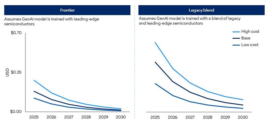
Source: Gartner (March 2026)
Falling Token Costs will not Democratize Frontier Intelligence
However, falling GenAI provider token costs will not be fully passed on to enterprise customers. Moreover, frontier intelligence will demand significantly more tokens than current mainstream applications. Agentic models, for example, require between 5-30 times more tokens per task than a standard GenAI chatbot, and can perform many more tasks than a human using GenAI.
While lower token unit costs will enable more advanced GenAI capabilities, these advancements will drive disproportionately higher token demand. As token consumption rises faster than token costs fall, overall inference costs are expected to increase.
“Chief Product Officers (CPOs) should not confuse the deflation of commodity tokens with the democratisation of frontier reasoning,” said Sommer. “As commoditised intelligence trends toward near-zero cost, the compute and systems needed to support advanced reasoning remain scarce. CPOs who mask architectural inefficiencies with cheap tokens today will find agentic scale elusive tomorrow.”
Value will accrue to platforms that can orchestrate workloads across a diverse portfolio of models. Routine, high-frequency tasks must be routed to more efficient small and domain-specific language models, which perform better than generic solutions at a fraction of the cost when aligned to specialised workflows. Expensive inference of frontier-level models must be heavily gated and reserved exclusively for high-margin, complex reasoning tasks.
The post Gartner Predicts That by 2030, Performing Inference on an LLM With 1 Trillion Parameters Will Cost GenAI Providers Over 90% Less Than in 2025 appeared first on ELE Times.
Keysight Launches Local Manufacturing in India to Accelerate Global Innovation
Keysight Technologies has announced plans to begin local manufacturing in India, expanding its global production footprint to provide locally manufactured solutions for the country’s mission-critical industries. This strategic expansion enables Keysight to better serve its long-standing customer base—including aerospace and defence, government R&D, industry and academic research institutions—by providing streamlined procurement of world-class technology.
As India emerges as one of the world’s fastest-growing innovation economies, demand for advanced test and measurement technologies is increasing across all industrial and research sectors. India’s electronics manufacturing sector is expected to exceed $300 billion by 2026, driven by a surge in domestic production and advanced research initiatives.
The phased rollout of the new facility will focus on test equipment, serving both Indian and global customers while enhancing supply chain resilience. The move reinforces Keysight’s long-term commitment to India and aligns with the country’s flagship initiatives, including Make in India, Semicon India, the National Quantum Mission, as well as aerospace and defence modernisation programs.
“India is entering a once-in-a-generation innovation decade,” said Sudhir Tangri, Vice President and General Manager, Asia Pacific at Keysight. “Establishing local manufacturing allows Keysight to better support customers in India while strengthening our global supply chain. Building in India for the world will accelerate technology development across a broad spectrum of industries.”
Keysight’s manufacturing operations in India will support innovation across key sectors:
- Semiconductors: Enabling design validation and production testing as India expands its semiconductor industry under the Semicon India program.
- Quantum Technologies: Supporting research institutions and national laboratories advancing quantum computing under the National Quantum Mission.
- Aerospace and Defence: Providing advanced, locally manufactured test solutions for radar, electronic warfare, and satellite systems supporting India’s defence modernisation.
- Next-Generation AI and Wireless: Accelerating development and deployment of 5G and future 6G infrastructure, AI infrastructure and data centres.
- Research and Academia: Equipping universities and national laboratories with world-class tools for advanced engineering research and scientific discovery.
Keysight will continue to collaborate with Indian government agencies, research laboratories, and leading engineering universities to accelerate technology development and strengthen the country’s innovation ecosystem. The expansion reflects Keysight’s long-term strategy to invest in high-growth technology hubs that support customers developing the next generation of computing, communications, and national security systems.
The post Keysight Launches Local Manufacturing in India to Accelerate Global Innovation appeared first on ELE Times.
Сторінки

