
ELE Times

The new performance bottleneck: How more GPU memory unlocks next-gen gaming and AI PCs
Courtesy: Micron
The next era of PC performance will be defined not by more compute, but by memory scale. The rising size of game assets and AI models has outpaced GPU memory capacity until now. Micron’s latest evolution of GDDR7 marks a pivotal shift for next-generation GPUs by combining higher memory density with the scalability that modern gaming and AI workloads now demand. With expanded capacity options built to support configurations up to 96GB of graphics memory, this generation of GDDR empowers systems to keep vastly larger worlds, richer textures, and growing AI models resident in memory, reducing bottlenecks and unlocking more consistent real-time performance across high-fidelity games and AI-enhanced applications.
Visual computing: The convergence of graphics and intelligence
Visual computing is entering a new era as graphics and intelligence converge. Modern systems must not only render high-fidelity scenes in real time, but also interpret, enhance, and generate content using increasingly complex AI models. Two forces are accelerating this shift: the push toward cinematic quality gaming and the rapid emergence of AI-powered PCs. As worlds grow larger, textures more detailed, and on-device AI more integral to responsiveness and personalisation, the demands placed on GPU memory have surged. What that means is, memory capacity and efficiency now determine how smoothly a system can deliver immersive gameplay, intelligent creation tools, and real-time simulation, making memory a foundational enabler of next-generation visual computing.
Delivering unprecedented performance for high-resolution gaming
Modern games are pushing GPU architectures harder than ever. Real-time ray tracing demands continuous access to massive datasets, geometry, materials, lighting maps, and shadows, while high refresh rate displays and ultra-resolution textures multiply the data the GPU must process each frame. Add in sprawling open worlds and increasingly AI-assisted rendering techniques, and the result is a workload that easily overwhelms traditional memory limits.
The problem is that when GPU memory can’t hold all this data at once, the system is forced to constantly swap assets in and out. That leads to the issues gamers know too well: texture pop-in, mid-frame stutters, uneven frame times, and sudden drops during intense ray-traced scenes. AI-generated frames and upscaling pipelines also become less consistent when memory is constrained, because the models and intermediate buffers they rely on are constantly competing for space.
This is where next-generation GDDR capacity and bandwidth become critical. By enabling far larger datasets to remain resident in memory, GDDR7 keeps the entire visual pipeline fed: textures, lighting data, geometry sets, and AI inference models, without the bottlenecks that cause visual artefacts or performance instability. The result is smoother, more predictable real-time rendering at 4K, 5K, and 8K, even in the most demanding scenes.
To keep these visual pipelines running efficiently, the memory subsystem must deliver data rapidly and consistently.
Enabling larger, more detailed worlds with 24Gb die density
As game environments expand and visual assets grow, memory capacity becomes critical to maintaining seamless, artefact-free experiences. Micron’s new 24Gb die density enables up to 96GB of graphics memory, giving GPUs significantly more space for high-resolution textures, expansive worlds, and advanced visual effects.
This increased capacity matters to gamers because:
- Reduces asset swapping and texture pop-in
- Supports larger frame buffers for high-resolution displays
- Enables richer, more detailed environments with fewer loading transitions
Creators and professional users also benefit from faster real-time rendering, more responsive GPU-accelerated workflows, and improved handling of large datasets.
Fueling AI-enhanced graphics and the rise of AI PCs
AI is rapidly becoming integral to personal computing. Neural rendering, real-time media enhancement, content generation, and AI-assisted workflows place new demands on system memory. Micron GDDR7 is built to support these emerging workloads with increased bandwidth, lower latency, and improved efficiency.
Why GDDR7 matters for AI PCs
AI-driven graphics and compute tasks rely on continuous movement of large datasets. GDDR7 accelerates these operations by improving throughput and responsiveness across GPU pipelines.
Systems built with GDDR7 benefit from:
- Faster on-device AI inference for creation, media, and collaboration
- Lower-latency performance across hybrid CPU-GPU-NPU workflows
- Higher throughput for neural graphics and generative AI models
- Improved power efficiency thanks to architectural refinements and reduced operating voltages
As AI becomes embedded into everyday PC tasks from writing, coding, editing, presenting, and gaming, memory performance will heavily influence the immediacy, intelligence, and fluidity of the experience.
Enabling the future of immersive and intelligent computing
Micron GDDR7 is more than a performance improvement; it is a foundational technology for the next decade of visual and AI computing. With 36 Gbps bandwidth, 24Gb die density, and improved efficiency, GDDR7 empowers GPU and AI PC vendors to deliver richer, more dynamic, and more intelligent computing experiences.
While NPUs are becoming essential for power-efficient, on-device AI acceleration, the most demanding visual and AI workloads still rely on the scale and parallelism of a discrete GPU. NPUs excel at sustained, low-power inference, but GPUs deliver significantly higher throughput for large models, neural graphics, advanced rendering, and gaming workloads. By pairing NPUs with discrete GPUs equipped with GDDR7, AI PCs can intelligently distribute tasks, assigning lightweight inference to the NPU while leveraging the GPU’s computing power and memory bandwidth for operations that require maximum performance. This combination unlocks capabilities far beyond what NPUs can achieve alone.
Together, Micron GDDR7 and the next wave of discrete GPUs set the stage for a new era of immersive graphics and high-performance AI computing.
The post The new performance bottleneck: How more GPU memory unlocks next-gen gaming and AI PCs appeared first on ELE Times.
Thermal Management in 3D-IC: Modelling Hotspots, Materials, & Cooling Strategies
Courtesy: Cadence
As three-dimensional integrated circuit (3D-IC) technology becomes the architectural backbone of AI, high-performance computing (HPC), and advanced edge systems, thermal management has shifted from a downstream constraint to a fundamental design driver. The dense vertical integration that enables unprecedented performance also concentrates heat at levels that traditional two-dimensional design methodologies cannot anticipate or mitigate. In fact, the temperatures and heat fluxes inside localised 3D-IC hotspots can approach fractions of those encountered in rocket-launching thermal zones, only here the challenge unfolds on a microscopic silicon landscape rather than within a combustion chamber. This extreme thermal intensity makes early and predictive planning essential rather than optional.
Effective thermal management now begins at the architecture definition stage, where designers evaluate stack feasibility, power distribution, and allowable thermal envelopes before committing to partitioning decisions. These early insights directly shape block placement, power-delivery topology, and the choice of materials, interposers, and packaging technologies. As the industry increasingly relies on vertically integrated systems to achieve performance-per-watt gains, thermal awareness emerges as an architectural discipline in its own right, one that guides every subsequent stage of the 3D-IC design flow.
This article guides modelling, estimating, and mitigating thermal challenges in dense stacks and interposer-based 3D-ICs, with an emphasis on early electrothermal strategies that scale with complexity.
Sources of Heat in Stacked Architectures
Heat in 3D-ICs arises from a combination of device activity, vertical power density, and material constraints. When logic, memory, and accelerators are stacked, the total power per unit footprint increases dramatically. Upper dies, which are furthest from the heatsink, experience higher thermal resistance and reduced cooling efficiency, creating natural hotspots even when their individual power numbers appear modest.
The placement of through-silicon via (TSV) arrays, micro-bumps, and interconnect pillars also shapes the heat landscape. These structures act not only as electrical conduits but also as thermal conduits, depending on the material and density. Die-to-die interfaces with bonding layers often introduce thermal bottlenecks, and when chiplets operate at different power states, steep thermal gradients can trigger stress and reliability concerns. Understanding these interactions early is essential for setting realistic thermal limits and performance expectations.
Early Compact Models and Power Map Estimation
Thermal analysis must begin in parallel with the architectural definition itself. Early-stage compact models enable architects to approximate temperature distributions using only high-level power budgets, long before physical implementation. By capturing the combined influence of die thickness, material stacks, bonding interfaces, and interposer conductivity, these models reveal whether planned power densities or proposed die-stack configurations are thermally realistic. They help flag infeasible assumptions early, ensuring that functional partitioning and stacking choices are guided by thermally credible boundaries rather than late-stage surprises.
Creating usable power maps at this stage does not require full register transfer level (RTL) activity vectors. Coarse workload profiles can yield first-order estimates of dynamic and leakage power. When combined with simplified geometry models, they highlight thermally sensitive regions, enabling design teams to adjust block partitioning, die assignment, and approximate placement before entering the detailed implementation phase.

Cadence’s multiphysics system analysis ecosystem connects power estimation, compact thermal model (CTM) modelling, and system-level thermal analysis, ensuring that signal, power, electromagnetic (EM), and thermal assumptions remain aligned throughout the early design phase. This early visibility reduces late-stage thermal surprises, which are often the costliest to rectify.
Heat Paths Through Dies, Interposers, and Package
Heat does not follow a single escape route in a 3D-IC. Instead, it propagates through a network of vertical and lateral paths whose efficiency depends on materials, die arrangement, and the package environment. Lower dies may benefit from direct contact with the heatsink, while upper dies rely on indirect conduction through intermediate layers. Thermal resistance builds cumulatively across each interface.
Interposers, whether made of silicon, glass, or organic materials, play a significant role in the heat flow picture. Silicon interposers offer superior thermal conductivity, enabling heat spreading but also concentrating thermal load where chiplets cluster. Organic interposers introduce more thermal resistance but offer other integration advantages. Achieving the correct tradeoff means modelling these layers as active participants in heat distribution, not static mechanical components.
The entire package, including substrate layers, heat spreaders, and lid materials, must also be included in thermal simulation. When package effects are omitted in early analysis, temperature predictions often skew optimistic, masking hotspots that emerge only after assembly-level modelling is performed.
Materials, TIMs, and Cooling Options for Stacks
Thermal simulation heavily relies on the structural definition of a product because the geometry, material properties, and assembly details directly dictate how heat is generated, transferred, and dissipated.
High-conductivity silicon, optimised interconnect materials, and improved underfill or bonding layers can lower the vertical thermal resistance of a stack. Thermal interface materials (TIMs) exhibit significant variations in performance, and even slight differences in thickness or coverage can result in substantial temperature differences across dies.
Cooling strategies for 3D-ICs are evolving rapidly. Traditional air cooling can be sufficient for moderate power budgets, but high-performance AI and HPC systems often require advanced approaches such as direct liquid cooling or vapour chamber solutions. The choice of cooling strategy should align with the power roadmap, not just the current generation’s requirements. Once a die stack is assembled, cooling options become constrained, so decisions made early influence the thermal feasibility of future product iterations.
Co-Optimisation with Placement and PDN Design
Thermal constraints directly influence floorplanning, macro placement, and power delivery network (PDN) topology in 3D-ICs. Efficient heat spreading is achieved when high-power blocks are positioned to maximise vertical conduction paths and lateral spreading through metal layers. If a block is placed too far from major thermal conduits, even robust cooling cannot compensate for the heat.
The PDN adds additional complexity. Power delivery structures, including TSVs, bumps, and interposer redistribution layers, introduce their own resistive heating. When modelled jointly with thermal effects, the combined electro-thermal behaviour reveals interactions that neither analysis can capture alone. Co-optimisation across these domains ensures that thermal mitigation does not compromise power integrity and vice versa.
A tightly integrated workflow enables round-trip refinement as power, placement, and package assumptions evolve. Without this iterative co-design, late-stage violations become inevitable, requiring disruptive redesigns.
Electro-Thermal Readiness for Signoff
Before committing a 3D-IC to final signoff, teams must verify that the design can withstand realistic thermal stress across operating modes and process corners. This includes validating that estimated power profiles align with actual activity, ensuring that predicted peak temperatures remain within safe limits, and confirming that no layer or interface exceeds its thermal reliability threshold.
Die-to-die boundaries, micro-bump arrays, TSV clusters, and package interconnects must be evaluated holistically, since minor thermal mismatches can accumulate into significant mechanical strain. Long-term reliability also depends on understanding how temperature interacts with electromigration, ageing, and performance drift over the product lifetime.
A complete electro-thermal signoff process provides the confidence needed before entering manufacturing, reducing field failures and ensuring long-term stability.
Designing for Thermal Scalability
3D-ICs deliver unprecedented performance, but they require a disciplined and predictive approach to thermal management. Success depends on treating heat as a first-order design variable, not a late-stage correction. Early modelling, accurate power estimation, careful material and stack selection, and co-optimisation across placement, PDN, interposer, and package all contribute to thermal resilience.
As system complexity continues to climb, teams that embed electro-thermal planning into their architecture and implementation flows will deliver higher-performing, more reliable, and scalable 3D-IC designs. Thermal awareness is no longer a specialisation; it is a foundational competency for next-generation semiconductor design.
The post Thermal Management in 3D-IC: Modelling Hotspots, Materials, & Cooling Strategies appeared first on ELE Times.
Keysight Launches AI Inference Emulation Platform to Validate and Optimise AI Infrastructure
Keysight Technologies has introduced Keysight AI Inference Builder (KAI Inference Builder), an emulation and analytics platform designed to validate inference-optimised AI infrastructure at scale. Keysight will demonstrate the solution at NVIDIA GTC, showcasing operation within NVIDIA DSX Air AI factory simulation environments to model and optimise AI data centre infrastructure, architectures, and performance.
As the AI industry shifts from training large language models (LLMs) to deploying them, optimising inference has become a crucial factor for ROI. However, inference behaviour is highly dynamic and difficult to emulate. Traditional testing methods like synthetic traffic generation or GPU benchmarks cannot accurately reproduce the latency-sensitive workload behaviour of AI inferencing across compute, networking, memory, storage, and security layers.
KAI Inference Builder closes that gap by recreating realistic inference workload patterns and modelling industry-specific usage patterns to validate AI infrastructure, applications, and data centre deployments. The platform gives AI cloud providers, hardware vendors, and application developers a scalable solution for measuring, validating, and optimising real-world inference performance.
Key benefits of KAI Inference Builder include:
Built for the Inference Era: As part of the Keysight Artificial Intelligence (KAI) portfolio, KAI Inference Builder emulates AI inference workloads at scale and validates full-stack deployments under real-world conditions to optimise performance, scale, and security.
- Industry- and Application-Specific Benchmarking: Instead of generic emulations, KAI Inference Builder emulates industry-specific usage patterns and LLM architectures for AI models seen in finance, healthcare, and other verticals, enabling organisations to model and analyse infrastructure and application behaviour across different types of AI data centre deployments.
- End-to-End Validation and Optimisation: KAI Inference Builder evaluates inference workflows from user request to model response, helping teams reduce costly rework by identifying and resolving bottlenecks early across compute, network, and security layers.
- Subsystem Isolation and Root-Cause Precision: KAI Inference Builder can also do client-only emulation, which identifies where performance bottlenecks emerge across the AI infrastructure stack under load, enabling targeted optimisation that reduces overprovisioning, lowers costs, and improves overall efficiency.
- NVIDIA DSX Air Integration and Live GTC Demo: Keysight will showcase KAI Inference Builder’s turnkey integration with NVIDIA Air at NVIDIA GTC, generating realistic inference workloads throughout NVIDIA’s data centre simulation environment so operators can validate inference infrastructure before deploying physical equipment.
Ram Periakaruppan, Vice President and General Manager, Network Test & Security Solutions at Keysight, said: “Inference is the key to unlocking AI’s ROI, but that can be challenging to achieve when system resources aren’t optimised for capacity and performance. KAI Inference Builder provides visibility into real-world inference performance across the full stack, enabling customers to validate and optimise deployments before hardware reaches the rack. Showcasing this capability at NVIDIA GTC using NVIDIA’s Air platform demonstrates how organisations can accelerate the path to production while reducing risk and cost.”
Amit Katz, VP of Networking at NVIDIA, said: “As AI data centres scale to unprecedented levels, pre-deployment validation has transitioned from a best practice to a mission-critical requirement. The integration of KAI Inference Builder with NVIDIA DSX Air provides the essential environment needed to eliminate performance volatility and enables NVIDIA AI Factory partners and customers to emulate real inference workloads and preemptively resolve bottlenecks, ensuring optimised AI services reach the market quickly.”
The post Keysight Launches AI Inference Emulation Platform to Validate and Optimise AI Infrastructure appeared first on ELE Times.
STMicroelectronics accelerates global adoption and market growth of Physical AI with NVIDIA
STMicroelectronics announced the acceleration of global development and adoption of physical AI systems, including humanoid, industrial, service and healthcare robots. ST is integrating its comprehensive portfolio for advanced robotics into the reference set of components compatible with the NVIDIA Holoscan Sensor Bridge (HSB). In parallel, high-fidelity NVIDIA Isaac Sim models of ST components are being integrated into both companies’ robotics ecosystems to support faster, more accurate sim-to-real research and development. The first deliverables available to developers today include the integration of Leopard’s depth camera enabled by ST with the NVIDIA HSB and the high-fidelity model of an ST IMU into NVIDIA’s Isaac Sim ecosystem.
“ST is well engaged within the robotics community, providing robust support and a well-established ecosystem,” said Rino Peruzzi, Executive Vice President, Sales & Marketing, Americas & Global Key Account Organization at STMicroelectronics. “Our collaboration with NVIDIA aims to unleash the next wave of cutting-edge robotics innovation with developer and customer experience streamlined at every step, from the inception of AI algorithms to the seamless integration of sensors and actuators. This will accelerate the evolution of sophisticated AI-driven physical platforms.”
“Accelerating the development of next-generation autonomous systems requires high-fidelity simulation and seamless hardware integration to bridge the gap between virtual training and real-world deployment,” said Deepu Talla, Vice President of Robotics and Edge AI at NVIDIA. “The integration of STMicroelectronics’ sensor and actuator technologies with NVIDIA Isaac Sim, Holoscan Sensor Bridge and Jetson platforms provides developers with a unified foundation to build, simulate and deploy physical AI at scale.”
Simplifying sensor and actuator integration with the Holoscan Sensor Bridge
With the NVIDIA HSB, developers can unify, standardise, synchronise, and streamline data acquisition and logging from multiple ST sensors and actuators, a critical foundation for building high-fidelity NVIDIA Isaac models, accelerating learning, and minimising the sim-to-real gap.
The goal is to simplify the process of connecting ST sensors and actuators to NVIDIA Jetson platforms through pre-integrated solutions for the combination of STM32 MCUs, advanced sensors (including IMUs, imagers, and ToF devices) and motor‑control solutions, particularly for humanoid robot designs. Leopard Imaging’s stereo depth camera for robots is the perfect example. Using ST imaging, depth and motion-sensing technologies, it is expected to support a broad wave of designs across Physical AI OEMs, academic research groups and the industrial robotics community.
Reducing cost, complexity, and challenges with high-fidelity modelling for Omniverse Isaac
Advanced robotics developers face high development costs, in addition to modelling challenges. High‑fidelity simulations with extensive randomisation demand substantial GPU and CPU resources and large datasets. Selecting which parameters to randomise, and over what ranges, requires deep domain expertise. Poor choices can result in unrealistic scenarios or inefficient training. Finally, excessive variability can confuse models, slow convergence, and degrade real‑world performance when randomisation no longer reflects plausible conditions.
ST and NVIDIA’s objective is to provide accurate, hardware-calibrated models for the comprehensive portfolio of ST components, matching the requirements of advanced robotics. Following the availability of the first model of an IMU, ST is working to bring developers models of ToF sensors, actuators and other ICs derived from benchmark data collected on real ST hardware, using ST tools to capture accurate parameters and realistic behaviour, resulting in models optimised to NVIDIA’s Isaac Sim ecosystem. NVIDIA HSB is being integrated into ST’s toolchain collaboratively.
As a result, ST and NVIDIA envision that more accurate models will significantly improve robot learning. With models that closely mirror real-world device behaviour, robots can learn from simulations that better reflect actual conditions, shortening training cycles and lowering the cost of building and refining humanoid robotics applications.
The post STMicroelectronics accelerates global adoption and market growth of Physical AI with NVIDIA appeared first on ELE Times.
Socomec Expands Power Solutions Portfolio in India, Launches MASTERYS GP4 UPS and ATyS a M Automatic Transfer Switch
Socomec has announced the launch of its new advanced MASTERYS GP4 UPS and ATyS a M Automatic Transfer Switch. This further strengthens their portfolio of reliable power management solutions. With over 25 years in the industry, the launch reinforces the company’s focus on innovative, efficient technologies for modern infrastructure.
Mr. Meenu Singhal, Regional Managing Director, Socomec Innovative Power Solutions, said,
“The launch of the MASTERYS GP4 UPS and ATyS a M Automatic Transfer Switch strengthens our portfolio with solutions that drive operational continuity and efficiency. From data centres and IT rooms to commercial buildings, organisations require resilient power infrastructure to ensure uninterrupted operations and protect critical systems. These products help optimise power supply while supporting reliable performance. We remain focused on innovation and committed to delivering dependable, future-ready power solutions for our customers.”
MASTERYS GP4 UPS, Designed for Critical Power Environments:
|
The Socomec MASTERYS GP4 200–250 kVA UPS is a high-performance uninterruptible power supply designed to ensure reliable power continuity for mission-critical environments. Built with advanced power protection technology and high-efficiency SiC technology, it delivers superior energy efficiency, consistent power quality, and reliable performance for data centres, industrial operations, and commercial infrastructure requiring uninterrupted operations. |
•Reliable power protection: Ensures uninterrupted power for critical infrastructure such as data centres, IT rooms, industrial processes, and commercial facilities, helping maintain operational continuity during grid disturbances.
•Advanced double-conversion technology: Provides stable and high-quality power output while minimising energy losses and supporting lower CO₂ emissions. • High efficiency and robust design: Combines high efficiency levels with a resilient architecture, leveraging advanced Sic technology to reduce downtime and support continuous operations in demanding environments. •Optimised for modern digital infrastructure: Designed to meet the growing power reliability needs of expanding digital ecosystems and industrial facilities. |
ATyS a M Automatic Transfer Switch: Compact, Reliable Source Switching:
|
Socomec’s ATyS a M Automatic Transfer Switch enables automatic and seamless switching between two power sources, such as the main utility supply and a backup generator, ensuring uninterrupted power for commercial buildings, industrial facilities and other critical installations where continuous operations are essential. |
•Automatic Source Transfer: Automatically switches between the main power source and backup supply, ensuring continuity of operations during power interruptions.
•Compact Modular Design: More compact than similar solutions, enabling easier integration within electrical panels and helping save valuable installation space. •Quick & Easy Commissioning: Integrated pre-configured controller automatically manages parameters and source transfers, reducing setup time and risk of manual error. •Proven Reliability for Low-Voltage Installations: Designed and tested according to international standards, supporting reliable switching for commercial and industrial facilities. |
Socomec offers support in design and commissioning, ensuring high-performing and sustainable electrical installations that are compliant. These solutions improve continuous power supply and strengthen resilience across data centres, industrial facilities, commercial buildings, and other critical infrastructure.
The post Socomec Expands Power Solutions Portfolio in India, Launches MASTERYS GP4 UPS and ATyS a M Automatic Transfer Switch appeared first on ELE Times.
EDOM Technology Strengthens Its Role in Integrating the Physical AI Ecosystem
EDOM Technology continues to expand its edge computing and intelligent system integration capabilities. Built on NVIDIA IGX Thor Development Kit, EDOM enables industries to adopt safety-critical computing platforms, accelerating the deployment of intelligent devices and autonomous computing systems while strengthening the physical AI competitiveness of Taiwan and the broader Asia-Pacific region.
With extensive system integration expertise, EDOM provides end-to-end hardware and software architecture planning, complemented by value-added engineering services that help customers streamline product development and deployment. Beyond computing platform advisory, EDOM also provides specialised services for safety-critical and sensor-rich edge environments, including functional safety architecture consulting, peripheral sensor and control module selection and integration, as well as ecosystem partner solution enablement. Through these capabilities and close collaboration with ecosystem partners, EDOM helps strengthen the industry value chain, lower technical integration barriers, and accelerate customers’ time to market.
The NVIDIA IGX Thor Platform is powered by NVIDIA Blackwell GPU architecture and supports NVIDIA Multi-Instance GPU (MIG) technology, enabling multiple AI workloads to run concurrently for improved resource utilisation. Designed to deliver high-performance edge AI computing, the platform achieves up to 5,581 FP4 TFLOPS of AI compute performance. Integrated with an Arm Neoverse CPU architecture, NVIDIA IGX Thor balances high-throughput AI inference with real-time data processing requirements, making it well-suited for deployment in a safety-critical environment.
NVIDIA IGX Thor Developer Kit also supports functional safety architecture implementation, incorporating compute monitoring and protection mechanisms to enhance long-duration operational stability. It also provides high-speed I/O connectivity and diverse expansion interfaces, facilitating integration with a wide range of sensing devices and industrial control modules. These capabilities address key edge computing requirements, including low latency, high reliability, and multi-sensor data integration.
As intelligent industry applications extend from cloud computing environments to physical devices, NVIDIA IGX Thor is well-suited for deployment in smart healthcare, industrial automation, and autonomous robotics. In smart manufacturing and industrial inspection scenarios, it supports real-time quality monitoring, predictive maintenance, and intelligent production line management. In healthcare environments, it enables high-precision imaging analysis and clinical decision support workloads. For autonomous mobile machines and service robots, its multi-sensor data fusion and real-time inference capabilities enhance navigation accuracy and safe obstacle avoidance.
Looking ahead, EDOM will continue to deepen its physical AI ecosystem integration services by combining hardware value-added integration expertise with an open partner collaboration model. Working alongside technology providers, system integrators, and application developers, EDOM aims to accelerate the deployment of edge AI computing solutions across diverse industry scenarios. By supporting customers from proof-of-concept validation through commercial rollout, EDOM enables the realisation of high-value AI-driven solutions and advances the evolution of next-generation smart industry value chains.
The post EDOM Technology Strengthens Its Role in Integrating the Physical AI Ecosystem appeared first on ELE Times.
Indian HVAC Market Poised to Double in Five Years with 15% Annual Growth
Industry leaders at ACREX India 2026 highlight that the Indian HVAC sector is poised for significant expansion, with the market expected to grow at 15% annually and potentially double within five years.
The industry is shifting toward local manufacturing and AI-driven predictive maintenance to capture massive growth potential in residential and infrastructure sectors. With residential AC penetration at just 10%, leaders are prioritising sustainability through humidity-optimised, super-efficient systems that can cut energy use by 60%. Ultimately, the sector is evolving beyond equipment sales to focus on the entire system lifecycle, emphasising energy efficiency, indoor air quality, and environmental impact.
Organised by ISHRAE, ACREX India 2026 served as a global hub where more than 400 exhibitors representing 40 nations and over 30,000 attendees gathered for South Asia’s premier HVAC and intelligent building exhibition. During the event, prominent industry leaders such as LG, Carrier, Daikin, Voltas, Danfoss, Schneider Electric, Panasonic, Johnson Controls and Tecumseh presented their latest advancements in next-generation cooling technology.
Speaking at the event, Mr Mukundan Menon, Managing Director, Voltas Limited, said, “The Indian HVAC industry is at the cusp of significant expansion, with the sector expected to grow at nearly 15% annually, potentially doubling within the next five years. Currently, about 15 million residential AC units are sold in India each year, and this is projected to reach around 30 million units by 2030. On the commercial side, India continues to build rapidly, creating strong opportunities across data centres, district cooling and infrastructure development. The recent GST reduction on ACs from 28% to 18% is a welcome policy step that will stimulate demand, with the first visible impact expected during the summer of 2026.”
Emphasizing the strong transformation and long-term growth potential of the HVAC industry in India, Mr Ravichandran Purushothaman, President, Danfoss Industries Private Limited, said, “Over the past three years, the HVAC industry in India has nearly doubled in size, with a significant shift toward local manufacturing, reflecting the momentum of Atmanirbhar Bharat and the government’s focus on reducing import dependence in the cooling sector. Looking ahead, the opportunity is substantial. As per the India Cooling Action Plan, cooling demand in India is expected to grow eightfold by 2038. On the commercial side, rapid expansion in semiconductor facilities, advanced manufacturing and data centres is driving demand for high-performance cooling solutions. At the same time, the industry is focusing on energy-efficient, water-efficient and carbon-efficient technologies, increasing localisation in electronics and strengthening new skill capabilities.”
Mr Jayanta Kumar Das, Society President, ISHRAE, said, “ACREX India brings the entire HVAC ecosystem onto one platform, enabling companies to showcase innovations and engage with the broader industry community. As cooling demand grows rapidly in India, the focus must move beyond equipment to the entire lifecycle of systems, where installation, operation and maintenance account for nearly 90% of the total cost. Through nationwide training programs, research and industry partnerships across 55+ locations, ISHRAE is working to strengthen skills, encourage innovation and support the sector’s mission of delivering more cooling with lower energy consumption and reduced environmental impact.”
Mr Amod Dikshit, Chairman, ACREX India, said, “India’s rapid infrastructure expansion and growing dependence on cooling across sectors such as data centres, district cooling, airports, hospitals, hotels and metro rail projects is creating a significant opportunity for the HVAC industry over the next decade. As this demand accelerates, the industry is focusing on localising the production of key sub-assemblies, strengthening capabilities and advancing more energy-efficient technologies. Cooling already accounts for nearly 40% of India’s electricity demand, which makes efficiency and sustainability critical priorities. With the Bureau of Energy Efficiency progressively upgrading standards every two years by about 7–10%, the industry continues to move towards more energy-efficient solutions.”
Ricardo Maciel, CEO of Tecumseh, said, “India is one of the world’s fastest-growing HVAC and refrigeration markets, fueled by urbanisation, food security, and expanding cold chain infrastructure. At ACREX, we highlighted our commitment to the Indian market through advanced, sustainable technology and strengthened local manufacturing. By combining global engineering with local production, we are meeting the market’s growing demand for energy efficiency, helping customers lower operating costs while supporting India’s long-term sustainability goals. Tecumseh introduced the new TC3 premium-efficiency compressor platform, ranging from 3 to 12 cc, delivering more than 30% energy savings compared to current platforms.”
Mr. Sanjeev Seth, Sr Vice President and Business Head, Systems Air Conditioning Division, LG Electronics India Limited, said, “India’s HVAC sector is on a strong growth trajectory, driven by rapid urbanisation, infrastructure expansion and increasing demand for efficient climate control. At the same time, AI is beginning to revolutionise HVAC system management in India, as customers seek higher energy efficiency and reduced downtime. Technologies such as predictive maintenance, cloud-based remote monitoring and intelligent controls are improving reliability and optimising energy consumption in VRF and chiller systems. This integration of digital technologies will significantly boost system performance and operational efficiency. At ACREX India 2026, LG Electronics India showcased its latest intelligent HVAC innovations designed for India’s evolving cooling landscapes. “
Mr. Abhishek Verma, Head – Products Marketing & Planning, Panasonic Life Solutions India Pvt. Ltd., said, “The air conditioning industry in India continues to offer strong growth potential. With residential AC penetration at around 8%, the segment has significant headroom for expansion and is expected to grow at a CAGR of nearly 15%, while the commercial AC market is also witnessing robust demand. As climate needs evolve, energy efficiency and indoor air quality are becoming key priorities. At Panasonic, we are advancing AI-driven cooling technologies to enhance energy efficiency without compromising comfort. At ACREX India, Panasonic showcased these intelligent and sustainable cooling solutions for India’s evolving needs.”
Globally, the HVAC industry is entering a significant expansion phase, with the market projected to reach nearly $445 billion by 2033, while HVAC systems already account for close to 40% of total building energy consumption worldwide. In response, the industry is rapidly shifting toward sustainable and energy-efficient technologies. Innovations such as AI-enabled smart HVAC systems, Variable Refrigerant Flow (VRF) technologies, natural refrigerants, district cooling systems, and advanced data centre cooling solutions are transforming the sector.
The post Indian HVAC Market Poised to Double in Five Years with 15% Annual Growth appeared first on ELE Times.
Smart EV Charging in India: How AI and ML Are Optimising Grid, Pricing and Reliability
India’s electric mobility transition is entering a decisive phase. While early discourse focused on vehicle innovation and battery chemistry, the spotlight has now shifted toward charging infrastructure, specifically, how intelligent systems can make it scalable, reliable, and grid-compatible. Artificial Intelligence (AI) and Machine Learning (ML) are no longer experimental add-ons; they are becoming the operational backbone of modern EV charging ecosystems.
From predictive maintenance and grid-responsive load management to dynamic pricing and battery safety modelling, Indian charging operators are embedding AI at every layer of infrastructure. Industry leaders such as Tata Power, Statiq, ChargeZone, and Bolt.Earth, Intellicar (Fabric IoT), and Coulomb AI are redefining what it means to deploy “smart” infrastructure in a high-growth, power-sensitive market like India.
AI-Driven Infrastructure Planning & Site SelectionCharging infrastructure planning in India can no longer rely on static demographic assumptions or simple traffic counts. With capital expenditure per fast-charging site running high, predictive intelligence has become central to ensuring ROI viability. AI-driven site selection models now ingest multi-layered datasets including vehicular density heatmaps, dwell-time patterns, telematics feeds, grid capacity data, and urban expansion forecasts to simulate demand even before physical deployment.
Such geospatial optimisation is particularly critical for India’s highway corridors and Tier-II cities, where deployment miscalculations can significantly impact utilisation rates. By integrating predictive analytics with grid feasibility mapping, operators are achieving measurable improvements in charger usage efficiency and long-term sustainability.
Predictive Maintenance & Reliability EnhancementReliability remains the most decisive performance metric in charging infrastructure. A single non-operational charger can undermine customer trust and disrupt fleet operations. AI-powered predictive maintenance is addressing this challenge by transforming chargers into continuously monitored, self-reporting assets.
Modern charging stations now incorporate IoT sensors that track temperature fluctuations, voltage irregularities, connector wear, vibration signatures, and cooling system performance. These data streams feed machine learning models capable of detecting anomaly patterns weeks before a component failure occurs.
Operators such as ChargeZone are leveraging AI-driven network management systems to monitor thousands of charging points simultaneously, ensuring SLA compliance and minimising revenue loss from unexpected outages. The result is not just improved uptime but a tangible reduction in ‘charge anxiety’ among users.
Smart Charging & Dynamic Load ManagementIndia’s distribution grids were not originally designed for high-density EV loads. Uncoordinated charging can create localised transformer stress and peak demand spikes. AI-driven smart charging systems are mitigating this risk by dynamically balancing load in real time.
By analysing grid capacity constraints, renewable energy availability, historical consumption curves, and user charging behaviour, AI systems intelligently stagger charging sessions without compromising user convenience. Time-of-Use (ToU) optimisation algorithms further encourage off-peak charging, reducing stress on urban feeders.
Pratik Kamdar, Co-founder & CEO of Neuron Energy: “AI and advanced software are emerging as the backbone of the modern EV ecosystem… [enabling] features such as real-time monitoring, predictive diagnostics, and faster charging capabilities that are increasingly prioritised by customers”.
Battery-integrated charging hubs deployed by ChargeZone further demonstrate how AI can shave peak demand and buffer grid volatility, a critical capability as EV adoption accelerates.
Dynamic Pricing & Revenue OptimisationThe economics of EV charging depend heavily on utilisation efficiency and tariff structuring. Traditional flat-rate pricing models often fail to respond to fluctuating grid conditions or consumer demand patterns. AI-powered dynamic pricing engines are now enabling real-time tariff modulation.
By factoring in grid stress indicators, occupancy rates, historical usage behaviour, and localised demand forecasts, AI models optimise pricing structures that balance revenue maximisation with consumer fairness.
Raghav Bharadwaj, CEO of Bolt.earth: On operational optimisation: “EV charging cannot be treated like a pure software startup… Every station’s economics must be optimised from day one. We measure success by uptime, utilisation, and energy delivered” (Source: Industry Perspectives).
Machine learning also supports customer segmentation, allowing differentiated pricing for fleet operators, subscription users, and retail consumers; thereby strengthening long-term business sustainability.
Vehicle-to-Grid (V2G) TechnologyVehicle-to-Grid technology introduces a paradigm shift in which EVs function as distributed energy storage assets capable of feeding electricity back into the grid. While regulatory frameworks in India are still evolving, AI is already playing a central role in enabling safe and optimised bidirectional charging.
AI algorithms determine optimal discharge windows, forecast grid demand spikes, and ensure battery health parameters remain within safe thresholds during V2G cycles. Without such intelligent orchestration, bidirectional charging could accelerate battery degradation.
As India moves toward distributed energy markets, AI-enabled V2G systems could unlock new revenue streams for EV owners and fleet operators alike.
Battery Safety & Thermal ManagementFast charging environments introduce elevated thermal risks, making battery safety paramount. AI-driven Battery Management Systems (BMS) are now capable of predicting thermal runaway scenarios before they escalate into critical failures.
Using chemistry-specific modelling and real-time telemetry data, machine learning algorithms estimate State-of-Charge (SoC) with accuracy exceeding 95% while simultaneously forecasting degradation patterns. This is particularly important given India’s mix of lithium iron phosphate (LFP) and nickel manganese cobalt (NMC) chemistries across vehicle categories.
Such advancements are not only improving safety but also extending battery lifecycle economics, a critical factor in total cost of ownership calculations.
User Experience EnhancementBeyond engineering efficiency, AI is reshaping the end-user journey. Intelligent routing systems now guide drivers to available chargers based on real-time occupancy predictions. Machine learning models calculate accurate charge time estimations by factoring in battery health, ambient temperature, and charger capacity.
Anshuman Divyanshu, CEO – EVSE, Exicom: “Ease comes from thoughtful design. Chargers and apps should feel intuitive… Selecting a connector, activating a session, pairing with an app, and making a payment. These steps shouldn’t feel like a technical exercise. A properly designed charger should operate like familiar everyday technology“.
Meanwhile, Statiq integrates predictive booking systems that mitigate congestion during peak hours. AI personalisation engines recommend preferred stations based on historical behaviour, payment patterns, and travel routes, creating a frictionless digital experience.
Cloud Computing & Edge AI IntegrationThe scalability of AI-driven charging infrastructure depends on a hybrid architecture that balances edge responsiveness with cloud intelligence. Edge computing processes latency-sensitive operations such as load modulation and fault isolation in real time, while cloud platforms handle macro-level optimisation, fleet analytics, and model retraining.
Arvind Gopalakrishnan, CTO & CIO at SUN Mobility: “We are leveraging AI to build robust, data-driven platforms that optimise EV charging, routing, and energy distribution across urban and intercity networks… enabling real-time decision-making and improving grid efficiency”.
Cybersecurity frameworks are also increasingly AI-driven, employing anomaly detection algorithms to identify spoofing attempts and data breaches in highly connected charging ecosystems.
The Road Ahead: 2026–2030As India moves toward deeper electrification, AI is poised to become the central nervous system of charging infrastructure. Self-healing networks, autonomous fleet charging depots, AI-integrated smart city command centres, and revenue-generating distributed energy marketplaces are no longer distant possibilities; they are emerging realities.
Khushboo Shrivastava, CEO of Coulomb AI, concludes, “The competitiveness of future charging networks will not be defined by hardware density alone, but by algorithmic intelligence. AI is what transforms infrastructure into an ecosystem.”
In the coming decade, India’s EV charging expansion will be defined less by the number of chargers deployed and more by the intelligence embedded within them. The evolution from hardware-centric infrastructure to software-defined energy ecosystems has already begun.
By: Shreya Bansal, Sub-Editor
The post Smart EV Charging in India: How AI and ML Are Optimising Grid, Pricing and Reliability appeared first on ELE Times.
Bengaluru Gets a World-Class Electronics Co-Innovation Hub as Henkel Launches Advanced Application Center
Henkel has announced the launch of its Customer Application Centre in Bengaluru, reinforcing its commitment to India’s rapidly expanding electronics manufacturing sector. The new facility will serve as a collaborative innovation hub where Henkel experts and customers can co-develop, test, and validate advanced adhesive and thermal management solutions for next-generation electronics manufacturing.
The new facility represents one of Henkel’s most significant application engineering commitments in the India Middle East and Africa (IMEA) region, and is designed to address a critical gap in India’s electronics value chain: the absence of localized, world-class application testing and validation infrastructure that allows manufacturers to develop, qualify, and scale advanced materials solutions without the time and cost of sending work overseas.
India’s electronics manufacturing sector has grown nearly sixfold over the past decade. The momentum is accelerating, driven by the rapid build-out of data centre and AI computing infrastructure, 5G and fibre network expansion, electric vehicle charging systems, industrial automation, and advanced medical devices. Each of these sectors depends critically on high-performance adhesives, thermal management materials, and protective coatings, and each demands faster, more localised application engineering support than India’s ecosystem has traditionally been able to provide.
Bengaluru was a natural choice. The city’s concentration of semiconductor design talent, electronics R&D centres, and global OEM engineering teams makes it the single most important node in India’s electronics innovation ecosystem. Locating the centre here puts Henkel’s application expertise directly alongside the engineers and manufacturers who need it most.
“India’s electronics manufacturing ecosystem is at an inflexion point, and Bengaluru is at the centre of it,” said S. Sunil Kumar, Country President – India, Henkel. “What manufacturers across our focus sectors increasingly need is not just world-class materials, but a local partner who can co-develop, test, and validate those materials under real production conditions, and help them move from concept to market faster. That is precisely what this centre is designed to do. It is our most tangible expression yet of Henkel’s long-term commitment to India’s electronics future.”
The 5,000 sq. ft. facility, of which approximately 2,400 sq. ft. is dedicated laboratory and testing space, is built to replicate actual electronics manufacturing conditions, allowing customers to evaluate and optimise materials and processes before committing to production scale. Around 60-65% of the investment has gone into advanced lab and testing equipment, with 20-25% directed at customer co-development infrastructure.
The facility serves five high-growth sectors: telecom and 5G infrastructure, data centres and AI computing, power electronics and EV systems, industrial automation, and medical electronics. Its key capabilities span advanced thermal management testing, precision dispensing systems, electrical characterisation tools, and rapid-cure chambers, supporting the full journey from prototyping and material validation through to production readiness.
The centre directly supports India’s Make-in-India and Production-Linked-Incentive objectives by bringing application engineering, process optimisation, and reliability validation onshore. A substantial share of activities that Indian electronics manufacturers previously had to route through overseas facilities, or simply defer, can now be conducted locally, compressing development cycles and accelerating time to market.
Henkel application experts will work side-by-side with customer engineering teams at the facility, co-developing solutions tailored to specific device architectures and manufacturing requirements. This collaboration model is central to the centre’s design and is what distinguishes it from a conventional testing laboratory.
The post Bengaluru Gets a World-Class Electronics Co-Innovation Hub as Henkel Launches Advanced Application Center appeared first on ELE Times.
Milestone Systems Redefines the Open Platform for an AI-Native Era
Milestone Systems has announced significant advancements to its XProtect video management software (VMS) and BriefCam video analytics. The XProtect App Platform, a new containerised application platform for VMS, and a new BriefCam analytics engine are designed to deliver increased reliability, greater customisation, more efficient hardware utilisation, and full readiness for Generative AI and analytics, empowering security teams to stay ahead as demands evolve.
Cameras and sensors collect more data than ever before. Today, the challenge has shifted from capturing information to understanding it – and turning it into actionable insight. Surfacing the most urgent threats and the most valuable operational insights requires AI and analytics tools built for the scale of modern video.
Even as capabilities advance, integrating new functionality still requires time, expertise, and coordination. Even routine software updates introduce operational risk. The possibility of system downtime often forces security teams to delay the very innovations that would make their operations more effective.
For solution developers creating the next generation of VMS applications, building and distributing solutions across thousands of customer environments adds another layer of complexity.
Milestone has built its new solutions to address these challenges – without requiring customers to replace what already works.
Building the Future of Video Management with the XProtect App Platform
Milestone’s new XProtect App Platform is a component that brings the latest VMS applications – including solutions like AI, analytics, access control, and more – into a surveillance system without friction.
The XProtect App Platform amplifies existing infrastructure by enabling customers to unlock insight from new AI tools, customise their systems quickly and safely, and install updates without downtime.
Built on a Linux-based, containerised architecture, the platform runs alongside existing XProtect installations and extends what the system can do without changing how it operates. Because each application and service runs in its own container, isolated from the core VMS and from other apps, customers can install apps and updates without requiring a full system restart or disrupting live operations.
Delivering next-generation analytics that scale with BriefCam’s new engine
BriefCam’s engine has been redesigned to deliver scalable analytics capabilities – with significant improvements to real-time processing, scalability, and workflow efficiency. Thanks to better resource utilisation, users will see an improvement of 38%* in real-time throughput. All processing can be run on-premise, with no cloud dependencies.
The new engine enables investigators to translate witness statements into searches using plain language instead of filters, identify key moments to reduce review time and turn fragmented video into a connected narrative, and train BriefCam with custom categorisations to match their organisational needs.
Andrew Burnett, Chief Technology Officer, Milestone Systems, said:
“The rapid growth of AI in video security has created an urgent need for platforms that can keep pace. Together with our partners and customers, we are co-creating the next generation of our technology on our open platform foundation. The XProtect App Platform and the new BriefCam engine are two major steps forward – giving organisations the flexibility to adapt quickly and confidently, as well as powerful on-premise intelligence that doesn’t compromise data sovereignty or operational control.”
Innovation across the ecosystem: App Centre and Developer Portal
The XProtect App Platform runs applications from the Milestone App Centre — the home for applications developed by both Milestone and our technology partners. The App Centre enables customers to browse, test, and install verified applications that extend the capabilities of their XProtect VMS. This makes it easier to discover new functionality, add AI analytics, or test emerging innovations without risk to live operations.
To support this, Milestone is introducing a new set of tools for developers and technology partners across the ecosystem. The Milestone Developer Portal consolidates everything developers need to build applications for the open platform in one place — from idea to development to release — providing a single, simple path to reach Milestone customers worldwide. The portal will be generally available by the end of 2026.
The XProtect App Platform and the new BriefCam engine are available now for early access customers. General availability is currently planned for late 2026.
The post Milestone Systems Redefines the Open Platform for an AI-Native Era appeared first on ELE Times.
NXP and NVIDIA Collaborate to Deliver New Innovations for Advanced Physical AI
NXP Semiconductors N.V. announced innovative robotics solutions for reliable, secure, real-time data processing and transport and advanced networking, enabling sensor fusion, machine vision and precision motor control. First in a series of NXP’s foundational robotics solutions, these ready-to-deploy solutions were developed in collaboration with NVIDIA and implement NVIDIA Holoscan Sensor Bridge with NXP’s highly integrated SoCs. This reduces discrete components, significantly shrinking footprint, power and cost, while also simplifying the software complexity of robotic sensing and actuation, including humanoid form factors.
Physical AI is the next frontier of innovation, featuring systems that can sense, interpret, and interact with their surroundings with precision, reliability and safety. Humanoid robots are one of the most advanced embodiments of physical AI, requiring secure, reliable, low-latency data processing and transport throughout the robot body to enable synchronised motion, dense sensor fusion and advanced actuation.
NXP’s new integrated robot body solutions directly address this challenge, delivering powerful edge intelligence and low-latency networking to enable safe, secure, real-time communication. These solutions seamlessly integrate NVIDIA Holoscan Sensor Bridge into NXP’s software enablement, allowing developers to easily implement real-time processing and establish a direct transport route between the body and pre-specified regions of the robot brain, substantially reducing latency. This significantly simplifies the challenges of bringing AI into the physical world, where real-time decision-making is a critical requirement.
“Physical AI is redefining what machines can do in the real world, and humanoid robots represent the most complex expression of that revolution,” said Charles Dachs, Executive Vice President and General Manager, Secure Connected Edge, NXP Semiconductors. “By combining NXP’s deep expertise in edge processing, secure networking, functional safety and real-time control with NVIDIA robotics platforms, we are greatly simplifying physical AI development, enabling seamless connectivity between the physical AI edge and the central brain. This is just the beginning of what NXP will deliver to accelerate the ecosystem for physical AI.”
“The development of autonomous machines requires a high-performance computing architecture that can synchronise complex motor controls with real-time perception,” said Deepu Talla, vice president of robotics and edge AI at NVIDIA. “By integrating NVIDIA Holoscan Sensor Bridge into its edge portfolio, NXP is providing developers with a scalable foundation to accelerate the deployment of physical AI.”
The collaboration between NXP and NVIDIA helps define a unified architecture for full-body humanoid robotics. NXP’s edge processors, motor control MCUs, automotive-grade networking technology, high-throughput asymmetric data transport capability acquired through Aviva Links, and functional safety expertise built on decades of automotive experience, combined with NVIDIA AI infrastructure, create a flexible, energy-efficient system architecture for next-generation robots.
The first Holoscan Sensor Bridge-ready solutions in NXP’s robotic portfolio include a machine vision solution based on the i.MX 95 applications processor delivering high-bandwidth data to the robot brain. It also includes a motor control solution based on a kinematic chain of i.MX RT1180 crossover MCUs, aggregated by NXP’s S32J TSN switch, directly connect to the brain. This motor control solution features integrated support for popular industrial protocols such as EtherCAT® and TSN. These flexible and software‑driven solutions are highly integrated to reduce footprint, power and cost, without sacrificing performance, safety or security, providing a complete, scalable foundation for full-body humanoid robot design.
The post NXP and NVIDIA Collaborate to Deliver New Innovations for Advanced Physical AI appeared first on ELE Times.
EDOM Showcases Physical AI & Robotics Applications at GTC 2026
EDOM Technology will participate in NVIDIA GTC for the third consecutive year under the theme “From AI to Action: Physical AI in Motion.” Together with ecosystem partners, EDOM will showcase its latest AI computing platforms, key components, and system integration capabilities. At Booth #242, EDOM will present physical AI and robotics solutions powered by NVIDIA Jetson hardware and software resources, demonstrating how AI technologies are being developed and deployed across diverse fields such as smart healthcare, vision recognition, and speech understanding. The showcase will highlight EDOM’s capability to connect the AI ecosystem and accelerate industry innovation through integrated solutions.
During the GTC exhibition, EDOM Technology plans to demonstrate several innovative applications that combine physical AI with edge computing. With the introduction of the NVIDIA Jetson Thor, AI inference and control architectures can now be integrated into a single system, providing a high-performance computing foundation for real-time closed-loop control and multimodal sensing, and accelerating the real-world deployment of multimodal intelligent robots.
In the robot interaction showcase, EDOM collaborates with Algoltek to present “Dexterous Hand AI.” Powered by 4D AI Vision technology and vision-action models, the system can recognise and predict audience hand gestures in real time and respond accordingly. This demonstration highlights low-latency AI inference and instant feedback, while also presenting a complete Sim-to-Real workflow, from virtual simulation to physical deployment. EDOM also partners with Nexuni to present “AI Workforce: Embodied Intelligence.” Built on the NVIDIA Thor platform, the system enables dual-arm robot manipulation through few-shot learning. The demonstration shows a service robot performing household tasks, including object recognition, grasping, and fabric folding. Because fabric is a highly deformable material, handling it requires complex visual perception, state estimation, and coordinated dual-arm control. By leveraging Jetson Thor’s edge AI inference and real-time dynamic path correction, the system continuously adjusts its movements during the folding process, improving task success rate and operational stability. This highlights the potential of physical AI in smart manufacturing, human-robot collaboration, and service robotics.
In the area of enterprise AI and smart biotech applications, EDOM collaborates with Avalanche Computing to showcase the “Secure Offline Generative AI” platform. Combining enterprise-grade private LLMs with real-time speech intelligence, the platform runs on the NVIDIA Jetson edge platform, enabling low-latency offline speech recognition and semantic analysis. This allows generative AI to deliver real-time interaction within highly secure enterprise environments. EDOM is also working with CyteSi to present the “Software-Defined High-Throughput Wet Lab,” an AI-driven laboratory automation platform. CyteSi’s EWOD (Electrowetting-on-Dielectric) technology digitally controls micro-droplets with precision, supporting workflows such as NGS sample preparation, drug discovery, and synthetic biology research. The system uses NVIDIA Jetson as its edge computing core, integrating biochips from Japan Display Inc. (JDI) with real-time image analysis capabilities to provide an intuitive user interface and highly efficient experimental workflow, advancing AI adoption in smart biotech research and automated laboratories.
In addition, EDOM will showcase the “NVIDIA Jetson Thor Peripheral Ecosystem,” integrating a range of EDOM-certified peripheral components, including high-speed storage, Wi-Fi 6/6E and 5G communication modules, GMSL and MIPI cameras, 10G high-speed networking, sensors, camera modules, and high-speed I/O interfaces. This ecosystem helps developers rapidly build next-generation robotics and physical AI systems. Through comprehensive hardware integration and platform support, EDOM assists robotics developers in accelerating product design, deployment, and mass production, further expanding the physical AI and Jetson Thor ecosystem.
Jeffrey Yu, CEO of EDOM Technology, stated, “The key to physical AI lies not only in computing performance, but in comprehensive hardware–software integration and ecosystem collaboration. Through NVIDIA’s Three-Computer architecture and the Jetson Thor platform, we help customers build scalable, production-ready, end-to-end AI solutions—from model training and simulation validation to edge deployment.” He further noted that EDOM is not just a hardware supplier, but is committed to integrating peripheral modules, AI software frameworks, and partner resources to help enterprises accelerate the adoption of AI and robotics technologies.
The post EDOM Showcases Physical AI & Robotics Applications at GTC 2026 appeared first on ELE Times.
Deep Learning-Based Predictive Maintenance: The Backbone of Smart Manufacturing 4.0
Unplanned downtime remains one of the most persistent and costly challenges in modern manufacturing. Studies and industry assessments from organisations such as Siemens and the Aberdeen Group have consistently shown that unexpected equipment failures cost global manufacturers tens of billions of dollars every year, with large automotive plants, semiconductor fabs, and energy facilities losing millions of dollars per hour during major production disruptions.
In the current manufacturing landscape, where production systems operate with minimal margins and global supply chains are under continuous pressure, downtime has evolved from a technical inconvenience to a significant strategic liability.
With the advent of Industry 4.0, manufacturing facilities have transitioned from isolated mechanical environments to complex digital ecosystems comprising interconnected machines, industrial electronics, sensors, software platforms, and automation. In this context, traditional maintenance approaches, such as reactive repairs or fixed-schedule servicing, are increasingly misaligned with contemporary operational requirements.
Predictive maintenance (PdM), enabled by deep learning and industrial artificial intelligence, is fundamentally transforming approaches to reliability in manufacturing. Rather than reacting to failures, organisations can now anticipate them, plan interventions proactively, and maintain uninterrupted production. Predictive maintenance, once considered a support function, is increasingly recognised as a core strategic capability.
From Rules to Learning: How Deep Learning Predicts FailuresEarlier predictive maintenance systems relied on fixed thresholds and rule-based logic—triggering alerts when temperature, vibration, or current crossed predefined limits. While effective for detecting obvious faults, these approaches were inherently reactive and struggled to capture the complex, nonlinear behaviour of modern equipment operating under variable loads and conditions.
Deep learning signifies a fundamental transition from rule-based systems to data-driven intelligence. Instead of relying on manually encoded expert assumptions, deep learning models extract knowledge directly from historical and real-time data, identifying subtle, multi-parameter patterns that precede failures, often weeks in advance and prior to the activation of conventional alarms. These early indicators are typically undetectable when individual signals are analysed in isolation.
In addition to enhancing prediction accuracy, deep learning facilitates a strategic shift toward probabilistic and horizon-based maintenance planning. Maintenance decisions are guided by remaining useful life estimates and associated confidence levels, rather than binary fault alerts, enabling teams to prioritise interventions, manage operational risk, and align maintenance actions with production objectives. Several deep learning techniques are now widely applied in industrial environments.
Convolutional Neural Networks (CNNs)CNNs are commonly used to analyse vibration spectrograms, thermal images, acoustic signatures, and visual inspection data. Subtle changes in these signals—often undetectable to human operators—can indicate early-stage bearing wear, imbalance, or surface degradation.
Recurrent Neural Networks (RNNs) and Long Short-Term Memory (LSTM) NetworksManufacturing equipment continuously generates time-series data from sensors embedded in motors, pumps, gearboxes, and actuators. LSTM models are particularly effective at learning long-term temporal dependencies, making them well-suited for predicting gradual wear, fatigue accumulation, and performance drift.
Autoencoders for Anomaly DetectionAutoencoders learn the normal operating behaviour of machines. When incoming data deviates from this learned baseline, the system flags anomalies that may signal emerging faults—even when labelled failure data is limited.
Practically, these models serve as digital reliability engineers by continuously monitoring assets and providing early warnings well in advance of potential production disruptions.
However, the effectiveness of learned intelligence is fundamentally dependent on the quality of the physical systems responsible for sensing, capturing, and transmitting data from the factory floor.
The Electronics Foundation Behind Predictive IntelligenceDeep learning-based predictive maintenance does not exist in isolation. Its effectiveness depends critically on the quality, reliability, and consistency of data originating from industrial electronics and sensing infrastructure. The performance of an AI model is fundamentally bounded by the fidelity of the signals it receives, which determines how accurately physical degradation mechanisms—such as bearing wear, insulation breakdown, or mechanical imbalance—are reflected in the data domain.
High-precision MEMS vibration sensors, thermal imaging modules, acoustic sensors, pressure sensors, and current-monitoring ICs form the data backbone of predictive systems. If these sensors are poorly calibrated, noisy, or inconsistently sampled, even the most advanced deep learning models will learn misleading patterns.
At the edge, industrial gateways and AI-capable processors facilitate local, low-latency analytics, thereby reducing reliance on cloud connectivity. This capability is particularly critical in sectors such as semiconductor manufacturing, automotive robotics, and power generation, where even milliseconds of delay or brief connectivity interruptions can result in significant consequences. In this context, sensors, edge processors, and industrial communication networks are foundational enablers of predictive intelligence rather than merely supporting components.
Industry Adoption: From Pilots to ProductionAcross sectors, deep learning-driven predictive maintenance is moving steadily from pilot projects to full-scale deployment.
Automotive ManufacturingAutomotive manufacturers increasingly apply AI-driven analytics to robotic assembly lines, analysing torque, vibration, and process parameters. These systems reduce unplanned downtime, stabilise quality, and support a transition from fixed maintenance schedules to condition-based strategies.
Aerospace and AviationRolls-Royce remains a reference point in this domain. Through its Engine Health Monitoring and Total Care programs, the company uses advanced analytics to anticipate component degradation, improve fleet availability, and enhance safety—demonstrating the long-term value of predictive intelligence in mission-critical systems.
Energy and UtilitiesPower plants rely on deep learning models to detect early signs of turbine imbalance, transformer insulation ageing, and rotating equipment faults. Early detection reduces outage risk and supports more reliable grid operations.
Electronics and Semiconductor ManufacturingIn semiconductor fabs, where uptime and yield are paramount, AI-based diagnostics monitor temperature stability, vibration, and process consistency. Predictive maintenance plays a central role in maintaining the precision required for advanced chip fabrication.
Industry Perspective: Insights from the FieldAccording to Sanjeev Srivastava, an industry spokesperson with extensive experience in industrial automation and intelligent manufacturing systems, the evolution of predictive maintenance reflects a deeper transformation in how manufacturers approach reliability and operational efficiency.
He observes that the transition from rule-based monitoring to learning-driven intelligence enables organisations to detect early-stage stress and degradation patterns that would otherwise remain invisible until failure. In this view, predictive maintenance is no longer a standalone analytics initiative but an integral part of how modern factories manage uptime, energy efficiency, and long-term asset performance.
This perspective aligns with a broader industry consensus that deep learning–based predictive maintenance is increasingly influencing strategic decision-making at the factory level, moving beyond experimental deployments.
Practical Challenges That Still MatterDespite its advantages, the implementation of deep learning–based predictive maintenance presents challenges that extend beyond algorithmic development. Frequently, organisational and data-related constraints are more formidable than the technological aspects.
Data Quality and ConsistencyDeep learning models require large volumes of reliable data. Poor sensor calibration, noise, and inconsistent sampling can significantly degrade prediction accuracy.
Legacy Equipment IntegrationMany factories operate a heterogeneous mix of new and ageing equipment that was never designed for continuous data sharing. Retrofitting sensors and integrating AI insights with existing PLCs, ERP, and MES systems requires careful engineering and cross-functional coordination.
Model Transparency and TrustMaintenance engineers with decades of experience are unlikely to act on AI recommendations without appreciating their rationale. Explainable AI techniques are, therefore, essential for building trust and encouraging adoption on the factory floor.
Scalability Throughout SitesModels trained in one plant may not transfer directly to another due to differences in equipment, operating conditions, and maintenance practices. Hybrid cloud–edge architectures and continuous retraining are essential for enterprise-wide deployment.
Cost constraints and return-on-investment timelines also significantly influence adoption, especially when predictive maintenance initiatives compete with other capital priorities within the plant.
The Road Ahead for Predictive MaintenanceSeveral trends are shaping the next phase of predictive maintenance:
- Edge AI for real-time, low-latency predictions
- Digital twins that simulate asset behaviour and support model training without disrupting production
- Federated learning to enable collaborative model improvement while preserving data privacy
- AI-driven maintenance orchestration linking predictions with scheduling and spare-part logistics
- Greater alignment with industrial standards such as IEC 62443 for cybersecurity and ISO 55000 for asset management
Digital twins provide substantial advantages; however, their effectiveness is contingent upon model fidelity and close synchronisation with real operational data. When anchored in live data rather than functioning as standalone simulations, digital twins serve as powerful tools for model training and workforce preparation without incurring downtime risks.
Edge AI, meanwhile, brings intelligence closer to the machine, enabling resilient, real-time decision-making even in connectivity-constrained environments. Together, these technologies are shaping more autonomous, responsive, and scalable maintenance systems.
Importantly, the future of predictive maintenance does not entail replacing engineers. Rather, artificial intelligence augments human expertise by managing continuous monitoring, anomaly detection, and early warning tasks at a scale unattainable by human teams alone.
Conclusion: A Strategic Shift, Not a Technology TrendDeep learning–based predictive maintenance is transforming the management of reliability, efficiency, and risk in the context of Smart Manufacturing 4.0. Through the integration of advanced algorithms, robust industrial electronics, and edge computing, organisations are able to anticipate failures, minimise downtime, extend asset lifespans, and enhance safety.
While challenges remain, momentum across industries is unmistakable. Advances in explainable AI, digital twins, and edge intelligence are accelerating adoption and lowering practical barriers.
Engineers continue to play a critical role in interpreting predictions, balancing safety with production priorities, and making high-impact decisions. In this collaboration between human judgment and machine intelligence, predictive maintenance can be realised. Within this context, deep learning–based predictive maintenance should be regarded not as an isolated artificial intelligence initiative, but as the foundational reliability backbone of Smart Manufacturing 4.0.ng 4.0 is being built.
The post Deep Learning-Based Predictive Maintenance: The Backbone of Smart Manufacturing 4.0 appeared first on ELE Times.
How Ethernet accelerates the move to software-defined vehicles
By: Madison Ecklund, systems manager, Body Electronics & Lighting
A zone architecture and Ethernet represent the future of networking in vehicles. New features in vehicles, as well as the shift to aggregating sensors and actuators into zonal control modules, require a high-bandwidth and low-latency in-vehicle communication network. A zone architecture implementing Ethernet enables the growing trend of the software-defined vehicle.
Most vehicles today are built using a type of wiring and electronic control unit (ECU) architecture called a domain architecture. A domain architecture categorises ECUs into domains based on specific functions, regardless of their physical location in the vehicle.
A zone architecture, in contrast to a domain architecture, organises communication, power distribution and load control by location rather than by function, as shown in Figure 1. A zonal control module behaves as a network data bridge between the vehicle’s computing system and local edge nodes such as smart sensors and ECUs. To reduce cabling in the vehicle, a zonal control module will also distribute power to different edge nodes (by implementing semiconductor smart fuse capabilities), handle low-level computing, and drive local loads such as motors and lighting.
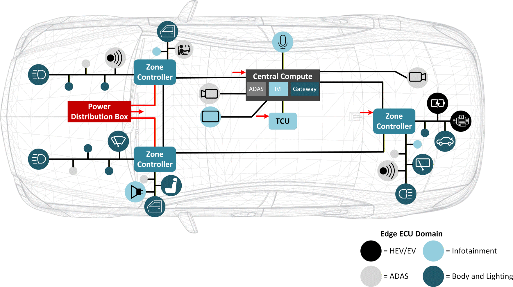 Figure 1. Example of a zone architecture
Zonal control modules transfer data from various sensors and ECUs through an edge-node communication network and forward the combined sensor data to the central computing system through backbone communication. Similarly, the zonal control modules transfer data received from the central computing system to various actuators, again through backbone communication, and again through an edge-node communication network. This two-way communication between the central computing system and the zonal control modules requires a high-bandwidth and low-latency communication backbone in order to handle the large amount of data generated by functions such as multiple advanced driver assistance system (ADAS) sensors, vehicle motion control and adaptive driving beams.
Bandwidth requirements in a zone architectureTo understand the value in using Ethernet in vehicles, let’s break down Ethernet use by application. The newly defined Single-Pair Ethernet supports speeds from 10Mbps to 10Gbps, defined through Institute of Electrical and Electronics Engineers (IEEE) 802.3cg (10Mbps), IEEE 802.3bw (100 Mbps), IEEE 802.bu (1Gbps) and IEEE 802.3ch (10Gbps). All of these new Ethernet technologies work over a single-pair cable and can communicate at distances as far as 15m, which is long enough to cover the longest link in a vehicle. Ethernet can also enable the time synchronisation of sensor data using IEEE 802.1AS timestamping to achieve low latency.
While Ethernet is capable of extremely fast speeds, these speeds are not necessary in every context. For example, communicating with the door control module or the heating, ventilation and air-conditioning system does not require a 100Mbps data rate. A 10Mbps Ethernet PHY, such as the DP83TD555J-Q1, or an alternative network protocol, such as Controller Area Network (CAN), is better for lower-speed and less bandwidth-intensive use cases, while reserving higher speeds for sending aggregated camera and autonomous driving sensor data from the zonal control modules to the central computing system. Figure 2 shows where to use different speeds of Ethernet in a zone architecture.
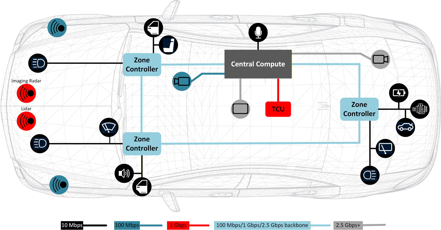 Figure 2. Ethernet in a zone architecture
Using Figure 2, let’s take a closer look at the communication speeds used for radar, lidar, camera and body applications. When the radar or lidar system-on-a-chip (SoC) processes the data, typically CAN, 10Mbps Ethernet or 100Mbps Ethernet communicates lidar or radar data to the zonal control module. When only first- or second-level data processing occurs, 100Mbps to 1Gbps Ethernet communicates radar and lidar data to the zonal module or central computer. Sending raw lidar or radar data to the central computing system for processing will extract more information through sensor fusion of various sensors. The transmission of such a large amount of raw data requires a higher bandwidth, typically a serial/deserializer (SerDes) protocol or 2.5Gbps plus Ethernet.
For cameras, SerDes such as Flat Panel Display (FPD)-Link is the most appropriate protocol when a level of increased ADAS data requires all of the raw data from the front camera for post-processing.
If it is possible to compress the data from the front camera and you don’t need this increased level of ADAS data, 100Mbps Ethernet is an alternative.
Body domain modules such as door handle sensors, window-lift control modules and side mirror control modules traditionally use the CAN and Local Interconnect Network (LIN) protocols to communicate, as neither requires a high bandwidth. While designers will continue to use CAN and LIN, the increased use of Ethernet in vehicles also creates a place for 10Mbps 10BASE-T1S multidrop Ethernet. Ethernet is traditionally a point-to-point topology, but 10BASE-T1S Ethernet is the first Ethernet standard enabling functionality over a bus topology.
Multigigabit Ethernet in a zone architectureWhat is the potential evolution of the zone architecture? It begins with aggregating body domain data, incorporating power distribution, and centralising computing. Over time, zone architectures will start aggregating data from other domains such as ADAS and infotainment. The end goal is to incorporate all domains into
the zone architecture. Regardless of which domain the data belongs to, the zonal control module and central computing system will still use the same backbone communication network to transfer data. Audio is a prime target to move into zone control modules, since it’s possible to transmit audio data over Ethernet with Audio Video Bridging standards.
Body domain functions typically require 10Mbps or less. But as ADAS or in-vehicle infotainment functions such as radar, lidar, audio and cameras become incorporated into the zone architecture, the speed and bandwidth requirements must increase and/or the Ethernet backbone topology may change from star to ring to accommodate the amount of safety-critical and time-sensitive sensor data.
Audio generates about 1.5Mbps per channel; a radar sensor typically generates 0.1Mbps to 15Mbps. Lidar generates 20Mbps to 100Mbps. Cameras generate the most 500Mbps to 3.5Gbps. Today’s vehicles typically have four to six radar sensors, one to five lidar sensors, 12 to 20 audio speakers, 12 to 16 audio microphones and six to 12 cameras. Table 1 shows the range of data generated by each type.
Table 1. Data generated in a zone architecture| Type | Data Generated | Quantity of Sensors | Low | Mid | High |
| Audio speaker | 1.5Mbps | 12 to 20 | 3.2Mbps | 24Mbps | 30Mbps |
| Audio microphone | 1.5Mbps | 12 to 16 | 3.2Mbps | 21Mbps | 24Mbps |
| Radar | 0.1 – 15Mbps | 4 to 6 | 0.4Mbps | 35Mbps | 90Mbps |
| Lidar | 20 – 100Mbps | 1 to 5 | 20Mbps | 100Mbps | 500Mbps |
| Camera | 500Mbps – 3.5Gbps | 6 to 12 | 3Gbps | 9Gbps | 42Gbps |
It is the total data being generated that is causing the push for 2.5Gbps, 5Gbps and 10Gbps Ethernet among original equipment manufacturers (OEMs). The zone architecture needs a backbone communication network capable of transmitting the enormous amount of data produced by ADAS sensors to the central computing system. Uncompressed camera data already goes beyond current Ethernet capabilities, and cameras continue increasing in resolution and pixel count. As vehicles continue toward autonomy, the number of sensors
will increase. Thus, the bandwidth required to support increased camera resolution and sensors will grow correspondingly.
The Ethernet speeds that OEMs are requesting most likely differ because of the transition schedules for incorporating different functions into the zonal control module. Audio playback on interior speakers is one of the first cross-domain data types adopted for use on the Ethernet backbone. This is likely caused by lower data generation in comparison, since 20 audio speaker channels generate about 30 Mbps. An existing 100Mbps or 1Gbps Ethernet backbone can easily accommodate the addition of audio playback data. Overall, the more high-level data functions in zonal control modules, the higher the bandwidth requirements.
Using Ethernet as the backbone for a zone architecture allows vehicles to transfer more data over the in-vehicle network when connecting to the internet or remote OEM servers. This enables subscription-based services and vehicle diagnostics through remotely performed firmware-over-the-air (FOTA) updates. FOTA updates allow for different hardware and software update cycles, which can be asynchronous as a result of the independence of sensors and actuators from the central computing node. A FOTA update can also push additional features and safety improvements, instead of waiting for a new model or having to bring the vehicle in to be worked on. Both the OEM and the customer benefit, as the OEM has control over updating the vehicle with additional features after launch, and the consumer is less inconvenienced by trips to a dealer to update firmware.
PHYs in a zone architectureEthernet requires the use of PHYs to transmit and receive high-speed data. Automotive Ethernet PHYs eliminate many of the concerns with Ethernet as the backbone of the wiring in vehicles, such as poor signal quality in
such a volatile environment. Ethernet PHYs from Texas Instruments (TI) are capable of operating at a range of temperatures from –40°C to 125°C, in compliance with Automotive Electronics Council-Q100 Grade 1 standards.
Ethernet PHYs also have to pass Ethernet compliance standards, ensuring that they meet certain interoperability and reliability standards regarding electromagnetic compatibility and electromagnetic interference, as well as IEEE conformance as specified by Open Alliance TC1 and TC12 standards, to work in a vehicular environment. With advanced diagnostic features such as signal quality indication, time domain reflectometry and electrostatic discharge sensors, PHYs are capable of detecting when errors occur and can identify these faults and enable the host system to respond proactively. For example, in the event of electrostatic discharge (ESD), the PHY sends an interrupt signal to the SoC and Media Access Control to alert it of the event and then checks other parts in the system.
Ethernet PHYs can also wake up remote ECUs over the Single-Pair Ethernet cable using the Open Alliance TC10 specification’s wake and sleep technology, which eliminates the need for a separate wire to wake
the ECUs from sleep. IEEE 802.1AE Media Access Control Security (MACsec) could also be an important technology to enable the authentication of networking ECUs and to encrypt/decrypt data to avoid cyberattacks, as cyberattacks represent the biggest threat to automotive networking.
Additional Ethernet PHYs include:
- TI’s DP83TC812-Q1, DP83TC815-Q1, and DP83TC814-Q1 100BASE-T1 PHYs have next-generation features suitable for luxury vehicles, while the smaller DP83TC813-Q1 100BASE-T1 PHY may be appealing in situations where printed circuit board space is at a premium. The DP83TG720-Q1 and DP83TG721-Q1 can connect zonal modules to data-intensive features such as the central computing system and telematics control unit, leaving headroom for the inclusion of additional features in later models without making intensive changes to the wiring harness. Combined, these PHYs open the door for more advanced and capable vehicles on the road.
- TI’s portfolio of Single-Pair Ethernet PHYs is designed to be footprint or pin-to-pin-compatible with both TI’s 100BASE-T1 and 1000BASE-T1. A single board design enables upgrades to the feature set or
bandwidth in future developments with no hardware changes. This approach helps accelerate development cycles, meet the requirements of different OEMs, and reduce time to market, thus saving R&D costs.
- The DP83TD555J-Q1 10BASE-T1S Serial Peripheral Interface MAC PHY integrates seamlessly into existing Ethernet backbone networks, eliminating protocol conversion gateways and their associated latency and processing overhead when connecting traditional CAN/LIN edge nodes. Supporting Power over Data Line, the device delivers both power and 10Mbps data over a single twisted-pair cable, reducing cable weight and system cost. Built-in PHY Collision Avoidance provides deterministic scheduling with guaranteed transmit opportunities for each network node, ensuring predictable communication timing. The larger Ethernet frame payloads enable extraction of higher data volumes and more diverse data types from ECUs at the vehicle’s edge, facilitating advanced diagnostics and over-the-air updates while maintaining real-time performance.
Advancements in automotive Ethernet technology will enable automakers to deliver more features and capabilities to new vehicles. A zone architecture implementing Ethernet will help accelerate the shift to software- defined vehicles by providing the data capacity that will support the next wave of autonomous features – leading to safer and smarter vehicles on the road.
The post How Ethernet accelerates the move to software-defined vehicles appeared first on ELE Times.
Intel Foundry Advances Chip Power Delivery with Next-Generation Capacitor Technology
Courtesy: Intel
Highlights
- Intel and Intel Foundry researchers demonstrated three promising metal-insulator-metal (MIM) materials delivering intrinsic capacitance density up to 98 femtofarads per square micrometre (fF/μm²), which is significantly higher than the 37 fF/um² intrinsic capacitance density of the material option used in state-of-the-art technology for more efficient chip power delivery.
- Compatible with advanced integrated MIM structures, these technologies deliver leakage well below targets while maintaining stable performance for over 400,000 seconds at elevated temperature, enabling multi-generational improvements without increasing manufacturing complexity.
- These process technology advances aid in the delivery of high performance per watt for chips ranging from data centres to mobile devices, continuing manufacturing efficiency improvements without added fabrication complexity.
Researchers at Intel and Intel Foundry have demonstrated next-generation decoupling capacitor (DCAP) materials that deliver substantial performance improvements for power delivery in advanced computer chips. Presented at the 2025 IEEE International Electron Devices Meeting (IEDM), the breakthrough takes advantage of unique metal-insulator-metal material properties. Ferroelectric hafnium zirconium oxide (HZO) leverages field-dependent dielectric response to achieve 60 to 80 fF/μm², while titanium oxide (TiO) and strontium titanium oxide (STO) reach 80 and 98 fF/μm² through ultra-high dielectric constants — each offering exceptional reliability with minimal voltage dependency.¹ All three materials show negligible capacitance drift over 100,000 seconds, leakage currents much lower than requirements, and 10-year projected breakdown voltages exceeding specifications at 90 degrees Celsius.
These advances have immediate implications for the semiconductor industry and the broader technology sector. Data centres processing artificial intelligence (AI) workloads can maintain high performance per watt longer with higher MIM decap, completing workloads faster while reducing data centre energy consumption and operation costs. Mobile devices benefit from reliable high performance and faster transitions to lower power states, leading to better battery efficiency. High-performance computing (HPC) systems gain processing headroom from a stable supply voltage, enabling maximum frequency for longer durations.
For chip manufacturers, these new capacitor materials offer a path to continue improving power delivery efficiency across multiple technology generations. The materials integrate seamlessly with existing backend manufacturing processes, enabling adoption without major retooling investments. Today’s advanced MIM capacitors often focus on architectural solutions similar to the state-of-the-art Omni MIM used in Intel 18A. Omni MIM has 397 fF/um² capacitance due to its deep-trench and multi-plate structure (see top image). By developing novel oxide materials that integrate seamlessly with these types of structures, the industry can unlock capacitance densities that exceed today’s benchmarks. These technologies help maintain the economic viability of advancing semiconductor manufacturing while meeting the escalating power delivery demands of next-generation processors, accelerators, and systems of chips designs.
The Challenge of Power Delivery in Advanced Chips
As chips pack more transistors into smaller spaces, maintaining stable power delivery grows increasingly difficult. When billions of transistors switch simultaneously, voltage can drop momentarily — called voltage droop — causing processors to slow, make errors, or run at reduced speeds. Decoupling capacitors solve this issue by acting as electrical reservoirs that instantly supply current when needed and absorb excess when demand drops.
Traditional approaches to increasing capacitance involve stacking multiple capacitor layers or etching deeper trenches to create more surface area. However, both significantly increase manufacturing complexity and cost. Material innovations offer an alternative by dramatically increasing the effective dielectric response, which is the material’s ability to store electrical charge. Finding materials with high effective dielectric constants that meet strict reliability requirements for years of operation at elevated temperatures represents a major materials science challenge.
Harnessing Ferroelectric Materials for Voltage-Responsive Capacitance
Ferroelectric hafnium zirconium oxide offers a unique property — the ability to store electrical charge changes with the applied electric field. Unlike conventional dielectrics, where this ability remains constant, ferroelectric materials contain microscopic regions called domains that orient themselves in response to electric fields, enabling different capacitance values at various operating voltages.
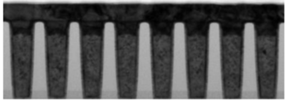
Figure 1. Transmission electron microscope image showing the deep-trench capacitor structure used to characterise the MIM stacks.
This type of testing requires careful attention to measurement methods. Under actual decoupling capacitor operation, where a constant bias voltage experiences small disturbances, the material shows remarkably stable capacitance independent of disturbance voltage, hold time, or number of pulses applied. The ferroelectric capacitors deliver 60 to 80 fF/μm² depending on operating voltage. Extensive reliability testing under various voltage levels, elevated temperatures of 90 degrees Celsius, and extended operation exceeding 400,000 seconds demonstrated negligible capacitance drift.
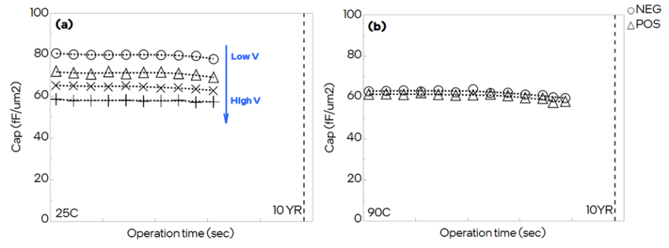
Figure 2. Capacitance measurements showing HZO’s stable, reliable performance under actual decoupling capacitor usage conditions.
Achieving Ultra-High Capacitance with Advanced Dielectric Materials
Titanium oxide and strontium titanium oxide provide even higher capacitance through extremely high dielectric constants with minimal voltage dependency. TiO achieves approximately 80 fF/μm², while STO reaches 98 fF/μm² — the highest demonstrated capacitance density.
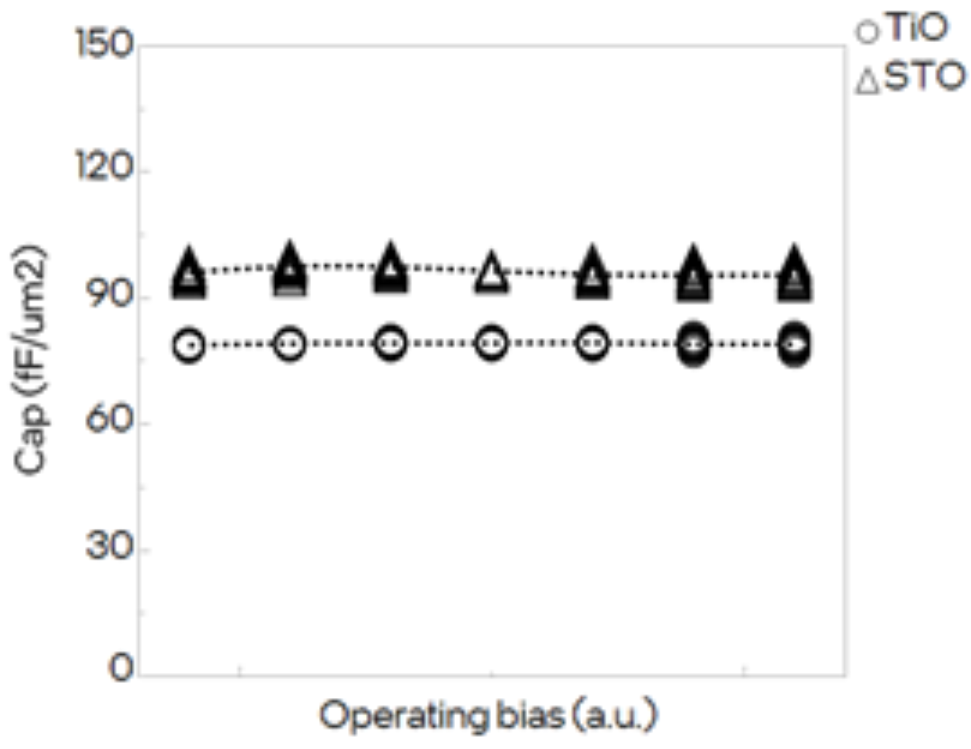
Figure 3. Capacitance versus voltage measurements showing weak voltage dependency across the operating range of interest.
Achieving these performance levels requires precise control over material structure at the atomic scale. The team developed optimised processes, including templating layers that guide crystal growth, controlling film deposition, thermal annealing that promotes desired crystal structure, and interface engineering to minimise defects. X-ray diffraction confirmed the successful production of strong high-dielectric-constant phases in both materials.
For TiO, detailed analysis reveals leakage current follows the Poole-Frenkel mechanism, where electrons trapped at defects gain energy from the electric field and hop between trap sites. This explains why the material withstands high currents without breaking down, with stress-induced leakage behaviour providing self-limiting protection against premature failure.
Exceptional Reliability Enables Multi-Layer Integration
All three materials demonstrate reliability exceeding decoupling capacitor requirements. Leakage current remains below targets even at 90 degrees Celsius. This is achieved through improved dielectric properties rather than making insulators thinner, which would increase leakage.
Time-dependent dielectric breakdown testing stressed devices at higher voltages and elevated temperatures, using statistical models to extrapolate expected lifetime. For HZO, extrapolation predicts operation exceeding high-voltage target spec for 10 years at 90 degrees Celsius with nearly identical breakdown behaviour regardless of voltage polarity. TiO also shows an extrapolated 10-year operating voltage significantly exceeding high-voltage requirements.¹ STO passes reliability targets for lower-voltage applications, though with larger variation due to deposition tooling requiring further optimisation.
The symmetric breakdown behaviour of HZO enables cost-effective multi-layer stacking where multiple capacitor layers connect in series, multiplying total capacitance without requiring complex integration schemes.
Looking Forward: Enabling Next-Generation Computing
This research demonstrates a clear path for continuous decoupling capacitor improvements across multiple semiconductor generations without increasing integration complexity. By improving intrinsic material properties rather than relying on structural innovations like deeper trenches or more layers, these approaches maintain manufacturing feasibility while delivering substantial performance gains.
The three materials provide flexibility for different requirements. HZO offers a practical, near-term option with reliability and straightforward integration. TiO serves as a successor with higher capacitance and exceptional high-voltage capability. STO represents the ultimate capacitance density for applications prioritising maximum capacitance.
Future work will focus on optimising these materials for manufacturing integration, refining deposition processes to improve uniformity, and exploring multi-layer stacking strategies. As computing advances toward AI accelerators, high-performance processors, and energy-efficient data centres, these capacitor technologies will play a vital role in enabling stable power delivery for next-generation semiconductor devices.
The post Intel Foundry Advances Chip Power Delivery with Next-Generation Capacitor Technology appeared first on ELE Times.
Keysight Partners with 3dB Labs to Enable Interoperable Signal Monitoring and Analysis
Keysight Technologies announced the integration of its spectrum analysers and FieldFox handheld analysers with 3dB Labs’ Sceptre, expanding interoperability between signal monitoring hardware and analysis software. The collaboration enables teams to monitor, analyse, and record radio frequency (RF) activity across mixed receiver environments within a unified workflow.
Teams operating in dense and contested RF environments often rely on equipment from multiple vendors while needing a consistent way to observe and interpret spectrum activity. By enabling Keysight instruments to operate directly within the Sceptre software environment, the integration reduces friction between measurement hardware and signal analysis workflows —allowing organisations to maintain multi-vendor receiver architectures while gaining a common platform for signal monitoring and investigation.
Sceptre supports real-time and offline spectrum and temporal analysis and connects receivers deployed on stationary or mobile collection platforms. When paired with Keysight analysers, users can monitor and characterise signals as they appear, capture activity for later playback, and analyse unknown or interfering signals to determine their nature and behaviour. The platform also supports unattended and remote operation, making it suitable for long-duration monitoring, RF surveys, and post-event analysis where access may be constrained.
Together, Keysight and 3dB Labs aim to strengthen the broader signal analysis ecosystem by promoting interoperability between measurement hardware and software-defined receiver platforms. Beyond improving day-to-day operations, the collaboration supports the development of more adaptable signal workflows, encourages integration across traditionally siloed tools, and helps teams build expertise that evolves as signal environments and mission demands change.
Dave Evans, President, 3dB Labs, Inc., said: “We are excited to partner with Keysight and integrate with their FieldFox handheld analysers, bringing Sceptre’s powerful signal detection, identification, and analysis capabilities to the tactical edge. We designed Sceptre for maximum interoperability, enabling teams to move from signal data to decisive action without bottlenecks, and together, we’re delivering an integrated solution that turns advanced signal processing into immediate mission advantage.”
Eric Taylor, Vice President of Aerospace, Defence and Government Solutions, Keysight, said: “Operational environments demand interoperability. By integrating Keysight analysers into multi-vendor ecosystems, teams can spend less time managing tools and more time understanding the spectrum. This integration brings together two leaders in the industry —Keysight in RF measurement and 3dB Labs in signal intelligence — to deliver advanced signal monitoring and analysis capabilities for our customers.”
The post Keysight Partners with 3dB Labs to Enable Interoperable Signal Monitoring and Analysis appeared first on ELE Times.
India to Boost Local Chip-making with a 1 Trillion Rupees Funding
India is expected to unveil a funding of more than a trillion rupees, nearly $10.8 billion, to fuel domestic chip-making. With 10 projects already approved, India aims to become a global manufacturing hub in the near future.
This new set of funds is expected to provide subsidies for chip designing projects, supply chain developments, and manufacturing equipment. Currently, the plan is under evaluation and may see the green light in a couple of months.
With the accelerated demand for chips driven by the rise of AI and electronics, the market is evolving at an exponential rate. Under the current leadership, India aims to position itself at the top to meet global demand.
With companies like Micron, TATA, and Foxconn already building India’s chip ecosystem, the country is expected to be close to industry leaders such as Taiwan and the US by 2032.
The post India to Boost Local Chip-making with a 1 Trillion Rupees Funding appeared first on ELE Times.
Qualitas Semiconductor Picks Anritsu’s Vector Network Analyzer for High-Speed Interconnect Signal Integrity Verification
Qualitas Semiconductor Co., Ltd., a leading developer specialising in PHY IP solutions for high-speed interconnects, has adopted Anritsu’s ShockLine 4-Port Performance Vector Network Analyzer (VNA) MS46524B to enhance signal integrity verification for its high-speed interface IP development. Qualitas has significantly improved the quality and reliability of its IP solutions by establishing a verification environment that enables highly accurate, repeatable signal-integrity evaluations across the entire system, including PHY IP.
Qualitas develops high-speed interface IP solutions, including SerDes PHY IP, PCI Express® PHY IP, UCIe interconnect solutions, and Ethernet PHY IP, and it collaborates with global customers across advanced semiconductor markets in fields such as AI, data centres, automotive, and mobile systems.
As semiconductor interface technologies continue to increase data transmission speeds, system-level verification that includes the characteristics of the entire interconnect channel, such as the PCB, package, and socket, has become increasingly important, rather than just the performance of the chips. In high-speed signal environments, factors such as transmission loss, reflection, and crosstalk affect signal integrity, making precise measurement-based verification environments essential.
To address these requirements, Qualitas has adopted Anritsu’s ShockLine MS46524B to analyse the characteristics of high-speed interconnect channels and quantitatively verify signal integrity, based on differential S-parameter analysis and time-domain reflectometry (TDR) measurements.
The ShockLine MS46524B provides high-frequency measurement stability, support for mixed probe and coaxial cable environments, and high-resolution TDR measurement capabilities, enabling precise analysis of subtle impedance variations occurring in the package and PCB structures. Through this approach, Qualitas has established a verification environment that is close to the conditions of real systems, enabling it to provide the reliability required in the PHY IP development process.
Anritsu highlights the importance of signal integrity verification solutions and measurement technologies that are required in next-generation interface technology environments, and it plans to support semiconductor and high-speed interface development companies in building more efficient verification environments.
The post Qualitas Semiconductor Picks Anritsu’s Vector Network Analyzer for High-Speed Interconnect Signal Integrity Verification appeared first on ELE Times.
The Tomorrow for AI and India’s edge advantage
Courtesy: Qualcomm
Artificial intelligence is entering its next chapter, one that reshapes not only how computing works, but how people experience technology in their daily lives. Intelligence is no longer just a feature, but is being built directly into devices and woven into systems and experiences so that it becomes ambient and always present.
In this next chapter, AI runs everywhere — across smartphones, PCs, wearables, cars, industrial machines, robots and connected infrastructure. These systems will understand context and the physical world around them and adjust in real time to our needs. Intelligence will operate quietly alongside us — working in the background, responding instantly, adapting continuously and ultimately expanding what’s possible in productivity, creativity and learning.
This marks a fundamental shift in how humans interact with technology. The interfaces we’ve relied on for decades — screens, apps, menus — will matter less as intelligence becomes more natural and intuitive. We won’t have to tell our devices what to do because they will understand our intent, anticipate what we want and act on our behalf. Some devices will increasingly see what we see, hear what we hear, understand what we read and write. In many cases, AI will feel less like a tool and more like a trusted assistant — always available, always learning and designed around us.
As agentic AI assistants become more common, they will become your personal companion in your home, the workplace and your car — everywhere you go. For example, in India, smart glasses are already being used to make digital payments using voice commands or by scanning a QR code. In your car, your AI assistant will not only help you find the fastest route but can also manage your errands, make recommendations or answer questions about places of interest.
In industries, edge AI boxes are being used to improve decision-making and operational efficiency, including monitoring and optimising production processes in a manufacturing facility or better managing inventory in a retail store.
Making these experiences real requires a new architecture — one where intelligence is distributed seamlessly across every computing device from cloud to edge. Training and deep reasoning will continue to scale in the cloud. At the same time, immediacy, perception and personalisation, as well as ambient and physical AI, will happen on devices — closer to people and things.
“To realise this future, democratizing access to AI is essential. That requires competitive and efficient data centre technology, powerful on-device intelligence and advanced connectivity working together.”
India’s size, diversity, economic growth and digital momentum make it one of the most important countries for AI’s next chapter. With hundreds of millions of connected users, a vibrant developer ecosystem, and deep expertise across engineering and software, India is not simply adopting AI — it is helping define how AI can work for the world.
In agriculture, AI can help enable precision farming and natural resource optimisation. Access to healthcare can be improved by on-device screening and diagnostics, which extend care into clinics, homes,s and remote communities. AI will realise the vision of smart cities with intelligent traffic management, smart infrastructure, security, and more. And, AI-enabled devices, such as PCs, smartphones, and wearables, will make education more personalised and support continuous, lifelong learning. These are not abstract ideas; they are practical pathways to broader participation in the AI economy.
To realise this future, democratizing access to AI is essential. That requires competitive and efficient data centre technology, powerful on-device intelligence, and advanced connectivity working together. It also requires an ecosystem approach — bringing together industry, startups, academia, and policymakers to ensure innovation is trusted, accessible,e and sustainable.
At Qualcomm, we’ve been building toward this future — advancing high-performance, power-efficient, and heterogeneous computing, AI, and wireless technologies that enable intelligence everywhere. But no single company can define AI’s next chapter alone. Progress will come through collaboration, from aligning technology with real-world needs, and from ensuring the benefits of AI extend beyond early adopters to entire societies.
With the right choices, India can help shape a future where intelligence empowers people, accelerates opportunity, and reaches every community — setting an example the world can follow.
The post The Tomorrow for AI and India’s edge advantage appeared first on ELE Times.
Posifa Technologies Introduces PVC4001-C MEMS Pirani Vacuum Transducer for Wide-Range Vacuum Measurement
Posifa Technologies has introduced its new PVC4001-C MEMS Pirani vacuum transducer, the latest device in the company’s PVC4000 series. Designed for cost-effective OEM integration, the transducer combines a MEMS thermal conduction sensor, measurement electronics, a microprocessor, and an onboard barometric pressure sensor in an ultra-compact PCB assembly with a connector-terminated wire harness.
Based on Posifa’s second-generation MEMS thermal conduction chip, the PVC4001-C operates on the principle that the thermal conductivity of gases is proportional to vacuum pressure. Its electronics and microprocessor amplify and digitise the sensor signal and provide output via an I²C interface. For applications requiring calibrated output, users can enter up to 10 pairs of calibration points, which are used by a built-in piecewise linearization algorithm.
The PVC4001-C is designed to deliver stable performance across changing operating conditions. A built-in temperature sensor supports a temperature compensation algorithm to offset changes in thermal conductivity caused by ambient temperature variation. In addition, a pulsed excitation scheme — in which the sensor is heated for about 100 ms and then turned off for one second — helps minimise drift due to self-heating in high vacuum, while also reducing power consumption for battery-powered instruments.
The device provides a measurement range from 0.001 Torr to 900 Torr (1.3*10-4 kPa to 120 kPa) with a response time of less than 200 ms. Because Pirani vacuum sensors typically lose resolution above 10 Torr, the PVC4001-C adds an onboard barometric pressure sensor that supports measurement from 10 Torr to 760 Torr with 5 % accuracy across that extended range. This combination makes the device especially well-suited for portable digital vacuum gauges and for leak detection in closed systems maintained under primary vacuum, including vacuum-insulated panels.
Additional features of the PVC4001-C include low power consumption, resistance to contamination, and an operating temperature range of -25 °C to +85 °C.
The post Posifa Technologies Introduces PVC4001-C MEMS Pirani Vacuum Transducer for Wide-Range Vacuum Measurement appeared first on ELE Times.
Сторінки

