
ELE Times

Modern Cars Will Contain 600 Million Lines of Code by 2027
Courtesy: Synopsys
The 1977 Oldsmobile Toronado was ahead of its time.
Featuring an electronic spark timing system that improved fuel economy, it was the first vehicle equipped with a microprocessor and embedded software. But it certainly wasn’t the last.
While the Toronado had a single electronic control unit (ECU) and thousands of lines of code (LOC), modern vehicles have many ECUs and 300 million LOC. What’s more, the pace and scale of innovation continue to accelerate at an exponential, almost unfathomable rate.
It took half a century for cars to reach 300 million LOC.
We predict the amount of software in vehicles will double in the next 12 months alone, reaching 600 million LOC or more by 2027.
The fusion of automotive hardware and software
Automotive design has historically been focused on structural and mechanical platforms — the chassis and engine. Discrete electronic and software components were introduced over time, first to replace existing functions (like manual window cranks) and later to add new features (like GPS navigation).
For decades, these electronics and the software that define them were designed and developed separately from the core vehicle architecture — standalone components added in the latter stages of manufacturing and assembly.
This approach is no longer viable.
Not with the increasing complexity and interdependence of automotive electronics. Not with the criticality of those electronics for vehicle operation, as well as driver and passenger safety. And not with a growing set of software-defined platforms — from advanced driver assistance (ADAS) and surround view camera systems to self-driving capabilities and even onboard agentic AI — poised to double the amount of LOC in vehicles over the next year.
From the chassis down to the code, tomorrow’s vehicles must be designed, developed, and tested as a single, tightly integrated, highly sophisticated system.
Shifting automotive business models
The rapid expansion of vehicular software isn’t just a technology trend — it’s rewriting the economics of the automotive industry. For more than a century, automakers competed on horsepower, handling, and mechanical innovation. Now, the battleground is shifting to software features, connectivity, and continuous improvement.
Instead of selling a static product, OEMs are adopting new, more dynamic business models where vehicles evolve long after they leave the showroom. Over-the-air updates can deliver new capabilities, performance enhancements, and safety improvements without a single trip to the dealer. And features that used to be locked behind trim levels can be offered as on-demand upgrades or subscription services.
This transition is already underway.
Some automakers are experimenting with monthly fees for heated seats or performance boosts. Others are building proprietary operating systems to replace third-party platforms, giving them control over the user experience — as well as the revenue stream. By the end of the decade, software subscriptions will become as common as extended warranties, generating billions in recurring revenue and fundamentally changing how consumers think about car ownership.
The engineering challenge behind OEM transformation
Delivering on the promise of software-defined vehicles (SDVs) that continuously evolve isn’t as simple as adding more code. It requires a fundamental rethinking of how cars are designed, engineered, and validated.
Hundreds of millions of lines of code must push data seamlessly across a variety of electronic components and systems. And those systems — responsible for sensing, safety, communication, and other functions — must work in concert with millisecond precision.
For years, vehicle architectures relied on dozens of discrete ECUs, each dedicated to a specific function. But as software complexity grows, automakers are shifting toward fewer, more powerful centralised compute platforms that can handle much larger workloads. This means more code is running on less hardware, with more functionality consolidated onto a handful of high-performance processors. As a result, the development challenge is shifting from traditional ECU integration — where each supplier delivered a boxed solution — to true software integration across a unified compute platform.
As such, hardware and software development practices can no longer be separate tracks that converge late in the process. They must be designed together and tailored for one another — well before any physical platform exists.
This is where electronics digital twins (eDTs) are becoming indispensable. By creating functionally accurate virtual models of vehicle electronics and systems, design teams can shift from late-stage integration to a model where software and hardware are co-developed from day one.
eDTs and virtual prototypes do more than enable earlier software development at the component level — they allow engineers to simulate, validate, and optimise the entire vehicle electronics. This means teams can see how data flows across subsystems, how critical components interact under real-world scenarios, and how emerging features might impact overall safety and performance. With eDTs, automakers can test billions — even trillions — of operating conditions and edge cases, many of which would be too costly, too time-consuming, or otherwise infeasible with physical prototypes.
By embracing eDTs, the industry is not just keeping pace with escalating complexity — it is re-engineering longstanding engineering processes, accelerating innovation, and improving the quality and safety of tomorrow’s vehicles.
The road ahead
Our prediction of cars containing 600 million lines of code by 2027 isn’t just a number. It signals a turning point for an industry that has operated in largely the same manner for more than a century.
Many automakers are reimagining their identity.
No longer just manufacturers, they’re becoming technology companies with business models that resemble those of cloud providers and app developers. They’re adopting agile, iterative practices, where updates roll out continuously rather than in multi-year product refreshes. And they’re learning how to design, develop, test, and evolve their products as a unified system — from chassis and engine to silicon and software — rather than a collection of pieces that are assembled on a production line.
Unlike the 1977 Oldsmobile Toronado, the car you buy in 2027 won’t be the same car you drive in 2030 — and that’s by design.
The post Modern Cars Will Contain 600 Million Lines of Code by 2027 appeared first on ELE Times.
Advancement in waveguides to progress XR displays, not GPUs
Across emerging technology domains, a familiar narrative keeps repeating itself. In Extended Reality (XR), progress is often framed as a race toward ever more powerful GPUs. In wireless research, especially around 6G, attention gravitates toward faster transistors and higher carrier frequencies in the terahertz (THz) regime. In both cases, this framing is misleading. The real constraint is no longer raw compute or device-level performance. It is system integration. This is not a subtle distinction. It is the difference between impressive laboratory demonstrations and deployable, scalable products.
XR Has Outgrown the GPU BottleneckIn XR, GPU capability has reached a point of diminishing returns as the primary limiter. Modern graphics pipelines, combined with foveated rendering, gaze prediction, reprojection, and cloud or edge offloading, can already deliver high-quality visual content within reasonable power envelopes. Compute efficiency continues to improve generation after generation. Yet XR has failed to transition from bulky headsets to lightweight, all-day wearable glasses. The reason lies elsewhere: optics, specifically waveguide-based near-eye displays.
Waveguides must inject, guide, and extract light with high efficiency while remaining thin, transparent, and manufacturable. They must preserve colour uniformity across wide fields of view, provide a sufficiently large eye-box, suppress stray light and ghosting, and operate at power levels compatible with eyewear-sized batteries. Today, no waveguide architecture geometric (reflective), diffractive, holographic, or hybrid solves all these constraints simultaneously. This reality leads to a clear conclusion: XR adoption will be determined by breakthroughs in waveguides, not GPUs. Rendering silicon is no longer the pacing factor; optical system maturity is.
The Same Structural Problem Appears in THz and 6GA strikingly similar pattern is emerging in terahertz communication research for 6G. On paper, THz promises extreme bandwidths, ultra-high data rates, and the ability to merge communication and sensing on a single platform. Laboratory demonstrations routinely showcase impressive performance metrics. But translating these demonstrations into real-world systems has proven far harder than anticipated. The question is no longer whether transistors can operate at THz frequencies; they can, but whether entire systems can function reliably, efficiently, and repeatably at those frequencies.
According to Vijay Muktamath, Founder of Sensesemi Technologies, the fundamental bottleneck holding THz radios back from commercialisation is system integration. Thermal management becomes fragile, clock and local oscillator integration grows complex, interconnect losses escalate, and packaging parasitics dominate performance. Each individual block may work well in isolation, but assembling them into a stable system is disproportionately difficult. This mirrors the XR waveguide challenge almost exactly.
When Integration Becomes Harder Than InnovationAt THz frequencies, integration challenges overwhelm traditional design assumptions. Power amplifiers generate heat that cannot be dissipated easily at such small scales. Clock distribution becomes sensitive to layout and material choices. Even millimetre-scale interconnects behave as lossy electromagnetic structures rather than simple wires.
As a result, the question of what truly limits THz systems shifts away from transistor speed or raw output power. Instead, the constraint becomes whether designers can co-optimise devices, interconnects, packaging, antennas, and thermal paths as a single electromagnetic system. In many cases, packaging and interconnect losses now degrade performance more severely than the active devices themselves. This marks a broader transition in engineering philosophy. Both XR optics and THz radios have crossed into a regime where system-level failures dominate component-level excellence.
Materials Are Necessary, But Not SufficientThis raises a critical issue for 6G hardware strategy: whether III–V semiconductor technologies such as InP and GaAs will remain mandatory for THz front ends. Today, their superior electron mobility and high-frequency performance make them indispensable for cutting-edge demonstrations.
However, relying exclusively on III–V technologies introduces challenges in cost, yield, and large-scale integration. CMOS and SiGe platforms, while inferior in peak device performance, offer advantages in integration density, manufacturability, and system-level scaling. Through architectural innovation, distributed amplification, and advanced packaging, these platforms are steadily pushing into higher frequency regimes. The most realistic future is not a single winner, but a heterogeneous architecture. III–V devices will remain essential where absolute performance is non-negotiable, while CMOS and SiGe handle integration-heavy functions such as beamforming, control, and signal processing. This mirrors how XR systems offload rendering, sensing, and perception tasks across specialised hardware blocks rather than relying on a single dominant processor.
Why THz Favours Point-to-Point, Not Cellular CoverageAnother misconception often attached to THz communication is its suitability for wide-area cellular access. While technically intriguing, this vision underestimates the physics involved. THz frequencies suffer from severe path loss, atmospheric absorption, and extreme sensitivity to blockage. Beam alignment overhead becomes significant, especially in mobile scenarios. As Mr Muktamath puts it, “THz is fundamentally happier in controlled environments. Point-to-point links, fixed geometries, short distances, that’s where it shines.”
THz excels in short-range, P2P links where geometry is controlled and alignment can be maintained. Fixed wireless backhauls; intra-data-centre communication, chip-to-chip links, and high-resolution sensing are far more realistic early applications. These use cases resemble the constrained environments where XR has found initial traction in enterprise, defence, and industrial deployments— rather than mass consumer adoption.
Packaging: The Silent DominatorPerhaps the clearest parallel between XR waveguides and THz radios lies in packaging. In XR, the waveguide itself is the package: it dictates efficiency, form factor, and user comfort. In THz systems, packaging and interconnects increasingly dictate whether the system works at all. Losses introduced by packaging can erase transistor-level gains. Thermal resistance can limit continuous operation. Antenna integration becomes inseparable from the RF front-end. This has forced a shift from chip- centric design to electromagnetic system design, where silicon, package, antenna, and enclosure are co-designed from the outset.
Communication and Sensing: Convergence with ConstraintsTHz also revives the idea of joint communication and sensing on shared hardware. In theory, high frequencies offer exceptional spatial resolution, making simultaneous data transmission and environmental sensing attractive. In practice, coexistence introduces non-trivial trade-offs.
Waveform design, dynamic range, calibration, and interference management all become more complex when reliability and throughput must be preserved. The most viable path is not full hardware unification, but carefully partitioned coexistence, with shared elements where feasible and isolation where necessary. This echoes XR architectures, where sensing and rendering share infrastructure but remain logically separated to maintain performance.
A Single Lesson Across Two DomainsXR waveguides and THz radios operate in different markets, but they are constrained by the same fundamental truth: the era of component-led innovation is giving way to system-led engineering. Faster GPUs do not solve optical inefficiencies. Faster transistors do not solve packaging losses, thermal bottlenecks, or integration fragility.
As Mr. Muktamath aptly concludes, “The future belongs to teams that can make complex systems behave simply, not to those who build the most impressive individual blocks.” The next generation of technology leadership will belong to organisations that master cross-domain co-design across devices, packaging, optics, and software. Manufacturability and yield as first-order design constraints, Thermal and power integrity as architectural drivers and Integration discipline over isolated optimisation. In both XR and THz, success will not come from building the fastest block, but from making the entire system work reliably, repeatedly, and at scale. That is the real frontier now.
The post Advancement in waveguides to progress XR displays, not GPUs appeared first on ELE Times.
AI-Enabled Failure Prediction in Power Electronics: EV Chargers, Inverters, and SMPS
Reliability is now a defining parameter for modern power electronic systems. As the world pushes harder toward electric mobility, renewable energy adoption, and high-efficiency digital infrastructure, key converters like EV chargers, solar inverters, and SMPS are running in incredibly demanding environments. High switching frequencies, aggressive power densities, wide bandgap materials (like SiC/GaN), and really stringent uptime expectations have all squeezed those reliability margins down to almost nothing. Clearly, traditional threshold-based alarms or basic periodic maintenance are no longer enough to guarantee stable operation.
This is exactly where AI-enabled failure prediction emerges as a breakthrough. By integrating real-time sensing, historical stress patterns, physics-based models, and deep learning, AI unlocks the ability to spot early degradation. This gives us the power to accurately estimate remaining useful life (RUL) and prevent catastrophic breakdowns long before they ever occur.
Jean‑Marc Chéry, CEO of STMicroelectronics, has emphasised that the practical value of AI in power electronics emerges at fleet and lifecycle scale rather than at individual-unit prediction level, particularly for SiC- and GaN-based SMPS.
Aggregated field data across large deployments is used to refine derating guidelines, validate device-level reliability models, and harden next-generation power technologies, instead of attempting deterministic failure prediction on a per-unit basis.
Limitations of Traditional Monitoring in Power Electronics
Conventional condition monitoring methods, things like simple temperature alarms, current protection limits, or basic event logs, operate reactively. They only catch failures after components have already drifted past the acceptable redline. Yet, converter failures actually start much earlier from subtle, long-term changes. Think about:
- Gradual ESR (Equivalent Series Resistance) increase in electrolytic capacitors
- Bond wire fatigue and solder joint cracking inside IGBT/MOSFET modules
- Gate oxide degradation in newer SiC devices
- Magnetic core saturation and insulation ageing
- Switching waveform distortions caused by gate driver drift
AI Techniques Powering Predictive Failure Intelligence
AI-based diagnostics in power electronics rest on three complementary pillars:
- Deep Learning for Real-Time Telemetry
AI-based diagnostics in power electronics rely on three complementary pillars:
Deep Learning for Real Time Telemetry Converters pump out rich telemetry data: temperatures, currents, switching waveforms, harmonics, soft switching behaviour, and acoustic profiles. Deep learning models find patterns here that are absolutely impossible for a human to spot manually.
- CNNs (Convolutional Neural Networks): These analyse switching waveforms, spot irregularities in turn-on/turn-off cycles, identify diode recovery anomalies, and classify abnormal transient events instantly.
- LSTMs (Long Short Term Memory Networks): These track the long-term drift in junction temperature, capacitor ESR, cooling efficiency, and load cycle behaviour over months.
- Autoencoders: learn the “healthy signature” of a converter and identify deviations that signal emerging faults.
- Physics-Informed ML
Pure machine learning struggles with operating points it has not seen; physics-informed machine learning offers better generalisation. It integrates:
- Power cycle fatigue equations
- MOSFET/IGBT thermal models
- Magnetics core loss equations
- Capacitor degradation curves
- SiC/GaN stress lifetime relationships
Peter Herweck, former CEO of Schneider Electric, has underscored that long-life power conversion systems cannot rely on data-driven models alone.
In solar and industrial inverters, Schneider Electric’s analytics explicitly anchor AI models to thermal behaviour, power-cycling limits, and component ageing physics, enabling explainable and stable Remaining Useful Life estimation across wide operating conditions.
- Digital Twins & Edge AI
Digital twins act as virtual replicas of converters, simulating electrical, thermal, and switching behaviour in real time. AI continuously updates the twin using field data, enabling:
- Dynamic stress tracking
- Load-cycle-based lifetime modelling
- Real-time deviation analysis
- Autonomous derating or protective responses
Edge-AI processors integrated into chargers, inverters, or SMPS enable on-device inference even without cloud connectivity.
AI-Driven Failure Prediction in EV Chargers
EV fast chargers (50 kW–350 kW+) operate under harsh conditions with high thermal and electrical stress. Uptime dictates consumer satisfaction, making predictive maintenance critical.
Key components under AI surveillance
- SiC/Si MOSFETs and diodes
- Gate drivers and isolation circuitry
- DC-link electrolytic and film capacitors
- Liquid/air-cooling systems
- EMI filters, contactors, and magnetic components
Roland Busch, CEO of Siemens, has emphasised that reliability in power-electronic infrastructure depends on predictive condition insight rather than reactive protection.
In high-power EV chargers and grid-connected converters, Siemens’ AI-assisted monitoring focuses on detecting long-term degradation trends—thermal cycling stress, semiconductor wear-out, and DC-link capacitor ageing—well before protection thresholds are reached.
AI-enabled predictive insights
- Waveform analytics: CNNs detect micro-oscillations in switching transitions, indicating gate driver degradation.
- Thermal drift modelling: LSTMs predict MOSFET junction temperature rise under high-power cycling.
- Cooling system performance: Autoencoders identify airflow degradation, pump wear, or radiator clogging.
- Power-module stress estimation: Digital twins estimate cumulative thermal fatigue and RUL.
Charging network operators report a 20–40% reduction in unexpected downtime by implementing AI-enabled diagnostics.
Solar & Industrial Inverters: Long-Life Systems Under Environmental Stress
Solar inverters operate for 10–20 years in harsh outdoor conditions—dust, high humidity, temperature cycling, and fluctuating PV generation.
Common failure patterns identified by AI
- Bond-wire lift-off in IGBT modules due to repetitive thermal stress
- Capacitor ESR drift affecting DC-link stability
- Transformer insulation degradation
- MPPT (Maximum Power Point Tracking) anomalies due to sensor faults
- Resonance shifts in LCL filters
AI-powered diagnostic improvements
- Digital twin comparisons highlight deviations in thermal behaviour or DC-link ripple.
- LSTM RUL estimation predicts when capacitors or IGBTs are nearing end-of-life.
- Anomaly detection identifies non-obvious behavior such as partial shading impacts or harmonic anomalies.
SMPS: High-Volume Applications Where Reliability Drives Cost Savings
SMPS units power everything from telecom towers to consumer electronics. With millions of units deployed, even a fractional improvement in reliability creates massive financial savings.
AI monitors key SMPS symptoms
- Switching frequency drift due to ageing components
- Hotspot formation on magnetics
- Acoustic signatures of transformer failures
- Leakage or gate-charge changes in GaN devices
- Capacitor health degradation trends
Manufacturers use aggregated fleet data to continuously refine design parameters, enhancing long-term reliability.
Cross-Industry Benefits of AI-Enabled Failure Prediction
Industries implementing AI-based diagnostics report:
- 30–50% reduction in catastrophic failures
- 25–35% longer equipment lifespan
- 20–30% decline in maintenance expenditure
- Higher uptime and service availability
Challenges and Research Directions
Even with significant progress, several challenges persist:
- Scarcity of real-world failure data: Failures occur infrequently; synthetic data and stress testing are used to enrich datasets.
- Model transferability limits: Variations in topology, gate drivers, and cooling systems hinder direct model reuse.
- Edge compute constraints: Deep models often require compression and pruning for deployment.
- Explainability requirements: Engineers need interpretable insights, not just anomaly flags.
Research in XAI, transfer learning, and physics-guided datasets is rapidly addressing these concerns.
The Future: Power Electronics Designed with Built-In Intelligence
In the coming decade, AI will not merely monitor power electronic systems—it will actively participate in their operation:
- AI-adaptive gate drivers adjusting switching profiles in real time
- Autonomous derating strategies extending lifespan during high-stress events
- Self-healing converters recalibrating to minimise thermal hotspots
- Cloud-connected fleet dashboards providing RUL estimates for entire EV charging or inverter networks
- WBG-specific failure prediction models tailored for SiC/GaN devices
Conclusion
AI-enabled failure prediction is completely transforming the reliability of EV chargers, solar inverters, and SMPS systems. Engineers are now integrating sensor intelligence, deep learning, physics-based models, and digital twin technology. This allows them to spot early degradation, accurately forecast future failures, and effectively stretch the lifespan of the equipment.
This whole predictive ecosystem doesn’t just cut your operational cost; it significantly boosts system safety, availability, and overall performance. As electrification accelerates, AI-driven reliability will become the core foundation of next-generation power electronic design. It makes systems smarter, more resilient, and truly future-ready.
The post AI-Enabled Failure Prediction in Power Electronics: EV Chargers, Inverters, and SMPS appeared first on ELE Times.
Powering AI: How Power Pulsation Buffers are transforming data center power architecture
Courtesy: Infineon Technologies
Microsoft, OpenAI, Google, Amazon, NVIDIA, etc. are racing against each other, and it is for good reasons: to build massive data centres with billions of dollars in investments.
Imagine a data centre humming with thousands of AI GPUs, each demanding bursts of power like a Formula 1 car accelerating out of a corner. Now imagine trying to feed that power without blowing out the grid.
That is the challenge modern AI server racks face, and Infineon’s Power Pulsation Buffer (PPB) might just be the pit crew solution you need.
Why AI server power supply needs a rethink
As artificial intelligence continues to scale, so does the power appetite of data centres. Tech giants are building AI clusters that push rack power levels beyond 1 MW. These AI PSUs (power supply units) are not just hungry. They are unpredictable, with GPUs demanding sudden spikes in power that traditional grid infrastructure struggles to handle.
These spikes, or peak power events, can cause serious stress on the grid, especially when multiple GPUs fire up simultaneously. The result? Voltage drops, current overshoots, and a grid scrambling to keep up.
 Figure 1: Example peak power profile demanded by AI GPUs
Rethinking PSU architecture for AI racks
To tackle this, next-gen server racks are evolving. Enter the power sidecar, a dedicated module housing PSUs, battery backup units (BBUs), and capacitor backup units (CBUs). This setup separates power components from IT components, allowing racks to scale up to 1.3 MW.
But CBUs, while effective, come with trade-offs:
- Require extra shelf space
- Need communication with PSU shelves
- Add complexity to the rack design
This is where PPBs come in.
What is a Power Pulsation Buffer?
Think of PPB as a smart energy sponge. It sits between the PFC voltage controller and the DC-DC converter inside the PSU, soaking up energy during idle times and releasing it during peak loads. This smooths out power demands and keeps the grid happy.
PPBs can be integrated directly into single-phase or three-phase PSUs, eliminating the need for bulky CBUs. They use SiC bridge circuits rated up to 1200 V and can be configured in 2-level or 3-level designs, either in series or parallel.
PPB vs. traditional PSU
In simulations comparing traditional PSUs with PPB-enhanced designs, the difference is striking. Without PPB, the grid sees a sharp current overshoot during peak load. With PPB, the PSU handles the surge internally, keeping grid power limited to just 110% of rated capacity.
This means:
- Reduced grid stress
- Stable input/output voltages
Better energy utilisation from PSU bulk capacitors
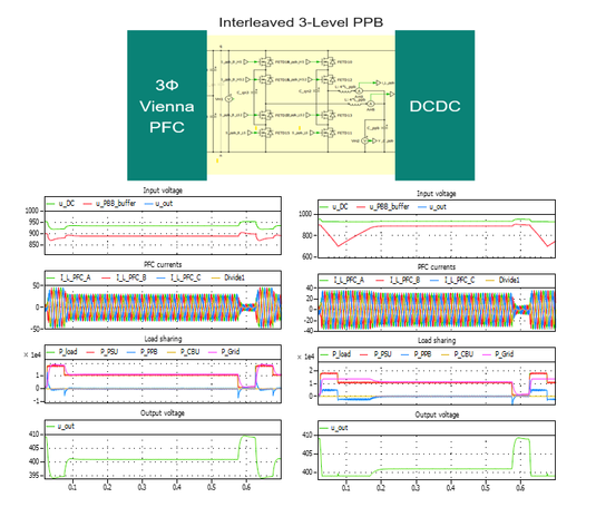 Figure 3: Simulation of peak load event: Without PPB (left) and with PPB (right) in 3-ph HVDC PSU
PPB operation modes
PPBs operate in two modes, on-demand and continuous. Each is suited to different rack designs and power profiles.
- On-demand operation: Activates only during peak events, making it ideal for short bursts. It minimises energy loss and avoids unnecessary grid frequency cancellation
- Continuous operation: By contrast, always keeps the PPB active. This supports steady-state load jumps and enables DCX with fixed frequency, which is especially beneficial for 1-phase PSUs.
Choosing the right mode depends on the specific power dynamics of your setup.
Why PPB is a game-changer for AI infrastructure
PPBs are transforming AI server power supply design. They manage peak power without grid overload and integrate compactly into existing PSU architectures.
By enhancing energy buffer circuit performance and optimising bulk capacitor utilisation, PPBs enable scalable designs for high-voltage DC and 3-phase PSU setups.
Whether you are building hyperscale data centres or edge AI clusters, PPBs offer a smarter, grid-friendly solution for modern power demands.
The post Powering AI: How Power Pulsation Buffers are transforming data center power architecture appeared first on ELE Times.
From Insight to Impact: Architecting AI Infrastructure for Agentic Systems
Courtesy: AMD
The next frontier of AI is not just intelligent – it’s agentic. As enterprises move toward systems capable of autonomous action and real-time decision-making, the demands on infrastructure are intensifying.
In this IDC-authored blog, Madhumitha Sathish, Research Manager, High Performance Computing, examines how organisations can prepare for this shift with flexible, secure, and cost-effective AI infrastructure strategies. Drawing on IDC’s latest research, the piece highlights where enterprises stand today and what it will take to turn agentic AI potential into measurable business impact.
Agentic AI Is Reshaping Enterprise Strategy
Artificial intelligence has become foundational to enterprise transformation. In 2025, the rise of agentic AI, systems capable of autonomous decision-making and dynamic task execution, is redefining how organisations approach infrastructure, governance, and business value. These intelligent systems don’t just analyse data; they act on it, adapting in real time across datacenter, cloud, and edge environments.
Agentic AI can reallocate compute resources to meet SLAs, orchestrate cloud deployments based on latency and compliance, and respond instantly to sensor failures in smart manufacturing or logistics. But as IDC’s July 2025 survey of 410 IT and AI infrastructure decision-makers reveals, most enterprises are still figuring out how to harness this potential.
IDC Insight: 75% Lack Clarity on Agentic AI Use Cases
According to IDC, more than 75% of enterprises report uncertainty around agentic AI use cases. This lack of clarity poses real risks where initiatives may stall, misalign with business goals, or introduce compliance challenges. Autonomous systems require robust oversight, and without well-defined use cases, organisations risk deploying models that behave unpredictably or violate internal policies.
Scaling AI: Fewer Than 10 Use Cases at a Time
IDC found that 83% of enterprises launch fewer than 10 AI use cases simultaneously. This cautious approach reflects fragmented strategies and limited scalability. Only 21.7% of organisations conduct full ROI analyses for proposed AI initiatives, and just 22.2% ensure alignment with strategic objectives. The rest rely on assumptions or basic assessments, which can lead to inefficiencies and missed opportunities.
Governance and Security: A Growing Priority
As generative and agentic AI models gain traction, governance and security are becoming central to enterprise readiness. IDC’s data shows that organisations are adopting multilayered data governance strategies, including:
- Restricting access to sensitive data
- Anonymising personally identifiable information
- Applying lifecycle management policies
- Minimising data collection for model development
Security testing is also evolving. Enterprises are simulating adversarial attacks, testing for data pollution, and manipulating prompts to expose vulnerabilities. Input sanitisation and access control checks are now standard practice, reflecting a growing awareness that AI security must be embedded throughout the development pipeline.
Cost Clarity: Infrastructure Tops the List
AI initiatives often falter due to unclear cost structures. IDC reports that nearly two-thirds of GenAI projects begin with comprehensive cost assessments covering infrastructure, licensing, labor, and scalability. Among the most critical cost factors:
- Specialised infrastructure for training (60.7%)
- Infrastructure for inferencing (54.5%)
- Licensing fees for LLMs and proprietary tools
- Cloud compute and storage pricing
- Salaries and overhead for AI engineers and DevOps teams
- Compliance safeguards and governance frameworks
Strategic planning must account for scalability, integration, and long-term feasibility.
Infrastructure Choices: Flexibility Is Essential
IDC’s survey shows that enterprises are split between building in-house systems, purchasing turnkey solutions, and working with systems integrators. For training, GPUs, high-speed interconnects, and cluster-level orchestration are top priorities. For inferencing, low-latency performance across datacenter, cloud, and edge environments is essential.
Notably, 77% of respondents say it’s very important that servers, laptops, and edge devices operate on consistent hardware and software platforms. This standardisation simplifies deployment, ensures performance predictability, and supports model portability.
Strategic Deployment: Data center, Cloud, and Edge
Inferencing workloads are increasingly distributed. IDC found that 63.9% of organisations deploy AI inference workloads in public cloud environments, while 50.7% continue to leverage their own datacenters. Edge servers are gaining traction for latency-sensitive applications, especially in sectors like manufacturing and logistics. Inferencing on end-user devices remains limited, reflecting a strategic focus on reliability and infrastructure consistency.
Looking Ahead: Agility, Resilience, and Cost-Efficient Infrastructure
As enterprises prepare for the next wave of AI innovation, infrastructure agility and governance sophistication will be paramount. Agentic AI will demand real-time responsiveness, energy-efficient compute, and resilient supply chains. IDC anticipates that strategic infrastructure planning can help in lowering operational costs while improving performance density by optimizing power and cooling demands. Enterprises can also avoid unnecessary spending through workload-aware provisioning and early ROI modelling across AI environments. Sustainability will become central to infrastructure planning, and semiconductor availability will be a strategic priority.
The future of AI isn’t just about smarter models; it’s about smarter infrastructure. Enterprises that align strategy with business value, governance, and operational flexibility will be best positioned to lead in the age of agentic intelligence.
The post From Insight to Impact: Architecting AI Infrastructure for Agentic Systems appeared first on ELE Times.
IIIT Hyderabad’s customised chip design and millimetre-wave circuits for privacy-preserving sensing and intelligent healthcare systems
In an age where governance, healthcare and mobility increasingly rely on data, how that data is sensed, processed and protected matters deeply. Visual dashboards, spatial maps and intelligent systems have become essential tools for decision-making, but behind every such system lies something less visible and far more fundamental: electronics.
Silicon-To-System Philosophy
At IIIT Hyderabad, the Integrated Circuits – Inspired by Wireless and Biomedical Systems, IC-WiBES research group led by Prof. Abhishek Srivastava, is rethinking how electronic systems are designed; not as isolated chips, but as end-to-end technologies that move seamlessly from silicon to real-world deployment. The group follows a simple but powerful philosophy: vertical integration from chip design to system-level applications.
Rather than treating integrated circuits, signal processing and applications as separate silos, the group works across all three layers simultaneously. This “dual-track” approach allows researchers to design custom chips while also building complete systems around them, ensuring that electronics are shaped by real-world needs rather than abstract specifications.
Why Custom Chips Still Matter
In many modern systems, off-the-shelf electronics are sufficient. But for strategic applications such as healthcare monitoring, privacy-preserving sensing, space missions, or national infrastructure, generic hardware often becomes a bottleneck. The IIIT-H team focuses on designing application-specific integrated circuits (ASICs) that offer greater flexibility, precision and energy efficiency than commercial alternatives. These chips are not built in isolation; they evolve continuously based on feedback from real deployments, ensuring that circuit-level decisions directly improve system performance.
Millimetre Wave Electronics
One of the lab’s most impactful research areas is millimetre-wave (mmWave) radar sensing, a technology increasingly used in automotive safety but still underexplored for civic and healthcare applications. Unlike cameras, mmWave radar can operate in low light, fog, rain and dust – all while preserving privacy. By transmitting and receiving high-frequency signals, these systems can detect motion, distance and even minute vibrations, such as the movement of a human chest during breathing.
Contactless Healthcare Monitoring
This capability has opened up new possibilities in non-contact health monitoring. The team has developed systems that can measure heart rate and respiration without wearables or cameras, which is particularly useful in infectious disease wards, elderly care, and post-operative monitoring. These systems combine custom electronics, signal processing and edge AI to extract vital signs from extremely subtle radar reflections. Clinical trials are already underway, with deployments planned in hospital settings to evaluate real-world performance.
Privacy-First Sensing For Roads
The same radar technology is being applied to road safety and urban monitoring. In poor visibility conditions, such as heavy rain or fog, traditional camera-based systems struggle. Radar-based sensing, however, continues to function reliably. The researchers have demonstrated systems that can detect and classify vehicles, pedestrians and cyclists with high accuracy and low latency, even in challenging environments. Such systems could inform traffic planning, accident analysis and smart city governance, without raising surveillance concerns.
Systems Shaping Chips
A defining feature of the lab’s work is the feedback loop between systems and circuits. When limitations emerge during field testing, such as signal interference or noise, the insights directly inform the next generation of chip designs. This has led to innovations such as programmable frequency-modulated radar generators, low-noise oscillators and high-linearity receiver circuits, all tailored to the demands of real applications rather than textbook benchmarks.
Building Rare Electronics Infrastructure
Supporting this research is a rare, high-frequency electronics setup at IIIT Hyderabad, capable of measurements up to 44 GHz – facilities available at only a handful of institutions nationwide. The lab has also led landmark milestones, including the institute’s first fully in-house chip tape-out and participation in international semiconductor design programs that provide broad access to advanced electronic design automation tools.
Training Full Stack Engineers
Beyond research outputs, the group is shaping a new generation of engineers fluent across the entire electronics stack- from transistor-level design to algorithms and applications. “Our students learn how circuit-level constraints shape system intelligence – a rare but increasingly critical skill,” remarks Prof. Srivastava. This cross-disciplinary training equips students for roles in national missions, deep-tech startups, academia and advanced semiconductor industries, where understanding how hardware constraints affect system intelligence is increasingly critical.
Academic Research to National Relevance
With sustained funding from multiple agencies, dozens of top-tier publications, patents in progress and early-stage technology transfers underway, the lab’s work reflects a broader shift in Indian research – one that is towards application-driven electronics innovation.
Emphasising that progress in deep-tech research isn’t linear, Prof. Srivastava remarks that at IC-WIBES, circuits, systems, and algorithms mature together. “Sometimes hardware leads. Sometimes applications expose flaws. The key is patience, persistence, and constant feedback. The lab isn’t trying to replace every component with custom silicon. Instead, we are focused on strategic intervention – designing custom chips where they matter most.”
The post IIIT Hyderabad’s customised chip design and millimetre-wave circuits for privacy-preserving sensing and intelligent healthcare systems appeared first on ELE Times.
Can the SDV Revolution Happen Without SoC Standardization?
Speaking at the Auto EV Tech Vision Summit 2025, Yogesh Devangere, who heads the Technical Center at Marelli India, turned attention to a layer of the Software-Defined Vehicle (SDV) revolution that often escapes the spotlight: the silicon itself. The transition from distributed electronic control units (ECUs) to centralized computing is not just a software story—it is a System-on-Chip (SoC) story.
While much of the industry conversation revolves around features, over-the-air updates, AI assistants, and digital cockpits, Devangere argued that none of it is possible without a fundamental architectural shift inside the vehicle. If SDVs represent the future of mobility, then SoCs are the engines quietly driving that future.
From 16-Bit Controllers to Heterogeneous Superchips
Automotive electronics have evolved dramatically over the past two decades. What began as simple 16-bit microcontrollers has now transformed into complex, heterogeneous SoCs integrating multiple CPU cores, GPUs, neural processing units, digital signal processors, hardware security modules, and high-speed connectivity interfaces—all within a single chipset.
“These SoCs are what enable the SDV journey,” Devangere explained, describing them as high-performance computing platforms that can consolidate multiple vehicle domains into centralized architectures. Unlike traditional ECUs designed for single-purpose tasks, modern SoCs are built to manage diverse functions simultaneously—from ADAS image processing and AI model deployment to infotainment rendering, telematics, powertrain control, and network management. This manifests a structural shift in the automotive industry.
Centralized Computing Is the Real Transformation
The move toward SDVs, in a way, is a move toward centralized computing. Simply stated, instead of dozens of independent ECUs scattered across the vehicle, OEMs are increasingly experimenting with domain controller architectures or centralized controllers combined with zonal controllers. In both cases, the SoC becomes the computational heart of the system, and this consolidation enables:
- Higher processing power
- Cross-domain feature integration
- Over-the-air (OTA) updates
- AI-driven functionality
- Flexible software deployment across operating systems such as Linux, Android, and QNX
A key enabler in this architecture is the hypervisor layer, which abstracts hardware from software and allows multiple operating systems to run independently on shared silicon. This flexibility is essential in a transition era where AUTOSAR (AUTomotive Open System ARchitecture) and non-AUTOSAR stacks coexist. AUTOSAR is a global software standard for automotive electronic control units (ECUs). It defines how automotive software should be structured, organized, and communicated, so that different suppliers and OEMs can build compatible systems.
But while the architectural promise is compelling, Devangere made it clear that implementation is far from straightforward.
The Architecture Is Not StandardizedOne of the most critical challenges he highlighted is the absence of hardware-level standardization. “Every OEM is implementing SDV architecture in their own way,” he noted. Some opt for multiple domain controllers; others experiment with centralized controllers and zonal approaches. The result is a fragmented ecosystem.
Unlike the smartphone world—where Android runs on broadly standardized hardware platforms—automotive SoCs lack a unified framework. There is currently no hardware consortium defining a common architecture. While open-source software efforts such as Eclipse aim to harmonize parts of the software stack, the hardware layer remains highly individualized. The consequence is complexity. Tier-1 suppliers cannot rely on long lifecycle platforms, as SoCs evolve rapidly. What might be viable today could become obsolete within a few years.
In an industry accustomed to decade-long product cycles, that volatility is disruptive.
Complexity vs. Time-to-MarketIf architectural fragmentation were not enough, development timelines are simultaneously shrinking. Designing with SoCs is inherently complex. A single SoC program often involves coordination among five to nine suppliers. Hardware validation must account for electromagnetic compatibility, thermal performance, and interface stability across multiple cores and peripherals. Software integration spans multi-core configurations, multiple operating systems, and intricate stack dependencies.
Yet market expectations continue to demand faster launches. “You cannot go back to longer development cycles,” Devangere observed. The pressure to innovate collides with the technical realities of high-complexity chip integration.
Power, Heat, and the Hidden Engineering BurdenBeyond software flexibility and AI capability lies a more fundamental engineering constraint: energy. High-performance SoCs generate significant heat and demand careful power management—critical in electric vehicles where battery efficiency is paramount. Many current architectures still rely on companion microcontrollers for power and network management, while the SoC handles high-compute workloads.
Balancing performance with energy efficiency, ensuring timing determinism across multiple simultaneous functions, and maintaining safety compliance remain non-trivial challenges. As vehicles consolidate ADAS, infotainment, telematics, and control systems onto shared silicon, resource management becomes as important as raw processing capability.
Partnerships Over IsolationGiven the scale of complexity, Devangere emphasized collaboration as the only viable path forward. SoC development and integration are rarely the work of a single organization. Semiconductor suppliers, Tier-1 system integrators, software stack providers, and OEMs must align early in the architecture phase.
Some level of standardization—particularly at the hardware architecture level—could significantly accelerate development cycles. Without it, the industry risks “multiple horses running in different directions,” as one audience member aptly put it during the discussion.
For now, that standardization remains aspirational.
The Real Work of the SDV EraThe excitement surrounding software-defined vehicles often focuses on user-facing features—AI assistants, personalized interfaces, downloadable upgrades. Devangere’s message was more grounded. Behind every seamless update, every AI-enabled feature, and every connected service lies a dense web of silicon complexity. Multi-core processing, heterogeneous architectures, thermal constraints, validation cycles, and fragmented standards form the invisible scaffolding of the SDV transformation.
The car may be becoming a computer on wheels. But building that computer—robust, safe, efficient, and scalable—remains one of the most demanding engineering challenges the automotive industry has ever faced.
And at the center of it all is the SoC.
The post Can the SDV Revolution Happen Without SoC Standardization? appeared first on ELE Times.
ElevateX 2026, Marking a New Chapter in Human Centric and Intelligent Automation
Teradyne Robotics today hosted ElevateX 2026 in Bengaluru – its flagship industry forum bringing together Universal Robots (UR) and Mobile Industrial Robots (MiR) to spotlight the next phase of human‑centric, collaborative, and intelligent automation shaping India’s manufacturing and intralogistics landscape.
Designed as a high‑impact platform for industry leadership and ecosystem engagement, ElevateX 2026 convened 25+ CEO/CXO leaders, technology experts, startups, and media, reinforcing how Indian enterprises are progressing from isolated automation pilots to scalable, business‑critical deployments. Ots)
Teradyne Robotics emphasized the rapidly expanding role of flexible and intelligent automation in enabling enterprises to scale confidently and safely. With industrial collaborative robots (cobots) and autonomous mobile robots (amr’s) becoming mainstream across sectors, the company underlined its commitment to driving advanced automation, skill development, and stronger industry‑partner ecosystems in India.
The event showcased several real‑world automation applications featuring cobots and amr’s across key sectors, including Automotive, F&B, FMCG, Education, and Logistics. These demos highlighted the ability of Universal Robots and MiR to help organizations scale quickly, redeploy easily, and improve throughput and workforce efficiency.
Showcasing high‑demand applications from palletizing and welding to material transport, machine tending, and training, the demonstrations reflected how Teradyne Robotics enables faster ROI, simpler deployment, and safe automation across high‑mix and high‑volume operations.
Speaking at the event, James Davidson, Chief Artificial Intelligence Officer, Teradyne Robotics, said, “Automation is entering a defining era – one where intelligence, flexibility, and human-centric design are no longer optional, but fundamental to how businesses innovate, scale, and compete. AI is transforming robots from tools that simply execute tasks into intelligent collaborators that can perceive, learn, and adapt in dynamic environments. In India, we are witnessing a decisive shift from experimentation to enterprise-wide adoption, and ElevateX 2026 reflects this momentum – bringing the ecosystem together to explore how collaborative and intelligent automation can become a strategic growth engine for both established enterprises and the next generation of startups.”
Poi Toong Tang, Vice President of Sales, Asia Pacific, Teradyne Robotics, added, “India is rapidly emerging as one of the most important and dynamic automation markets in Asia Pacific. Organizations today are not just looking to automate – they are looking to build operations that are flexible, resilient, and future-ready. The demand is for modular automation that delivers faster ROI and can evolve alongside business needs. Through Universal Robots and MiR, we are enabling end-to-end automation across production and intralogistics, helping Indian companies scale with confidence and compete on a global stage.”
Sougandh K.M., Business Director – South Asia, Teradyne Robotics, said, “India’s automation journey will be defined by collaboration across its ecosystem — by partners, system integrators, startups, and skilled talent working together to turn technology into real impact. At Teradyne Robotics, our belief is simple: automation should be for anyone and anywhere, and robots should enable people to do better work, not work like robots. Our focus is on automating tasks that are dull, dirty, and dangerous, while helping organizations improve productivity, safety, and quality. ElevateX 2026 is about lowering barriers to adoption and building long-term capability in India, making automation practical, scalable, and accessible, and positioning Teradyne Robotics as a trusted partner in every stage of that growth journey .”
Customer Case Story Testimonial/Teaser
A key highlight of ElevateX 2026 was the spotlight on customer success, and Origin stood out. As a fast‑growing U.S. construction tech startup, they shared how partnering with Universal Robots is driving measurable impact through improved productivity, stronger safety, and consistently high‑quality project outcomes powered by collaborative automation.
Yogesh Ghaturle, the Co-founder and CEO of Origin, said, “Our goal is to bring true autonomy to the construction site, transforming how the world builds. Executing this at scale requires a technology stack where every component operates with absolute predictability. Universal Robots provides the robust, operational backbone we need. With their cobots handling the mechanical precision, we are free to focus on deploying our intelligent systems in the real world.”
The post ElevateX 2026, Marking a New Chapter in Human Centric and Intelligent Automation appeared first on ELE Times.
The Architecture of Edge Computing Hardware: Why Latency, Power and Data Movement Decide Everything
Courtesy: Ambient Scientific
Most explanations of edge computing hardware talk about devices instead of architecture. They list sensors, gateways, servers and maybe a chipset or two. That’s useful for beginners, but it does nothing for someone trying to understand how edge systems actually work or why certain designs succeed while others bottleneck instantly.
If you want the real story, you have to treat edge hardware as a layered system shaped by constraints: latency, power, operating environment and data movement. Once you look at it through that lens, the category stops feeling abstract and starts behaving like a real engineering discipline.
Let’s break it down properly.
What edge hardware really is when you strip away the buzzwords
Edge computing hardware is the set of physical computing components that execute workloads near the source of data. This includes sensors, microcontrollers, SoCs, accelerators, memory subsystems, communication interfaces and local storage. It is fundamentally different from cloud hardware because it is built around constraints rather than abundance.
Edge hardware is designed to do three things well:
- Ingest data from sensors with minimal delay
- Process that data locally to make fast decisions
- Operate within tight limits for power, bandwidth, thermal capacity and physical space
If those constraints do not matter, you are not doing edge computing. You are doing distributed cloud.
This is the part most explanations skip. They treat hardware as a list of devices rather than a system shaped by physics and environment.
The layers that actually exist inside edge machines
The edge stack has four practical layers. Ignore any description that does not acknowledge these.
- Sensor layer: Where raw signals are produced. This layer cares about sampling rate, noise, precision, analogue front ends and environmental conditions.
- Local compute layer: Usually MCUs, DSP blocks, NPUs, embedded SoCs or low-power accelerators. This is where signal processing, feature extraction and machine learning inference happen.
- Edge aggregation layer: Gateways or industrial nodes that handle larger workloads, integrate multiple endpoints or coordinate local networks.
- Backhaul layer: Not cloud. Just whatever communication fabric moves selective data upward when needed.
These layers exist because edge workloads follow a predictable flow: sense, process, decide, transmit. The architecture of the hardware reflects that flow, not the other way around.
Why latency is the first thing that breaks and the hardest thing to fix
Cloud hardware optimises for throughput. Edge hardware optimises for reaction time.
Latency in an edge system comes from:
- Sensor sampling delays
- Front-end processing
- Memory fetches
- Compute execution
- Writeback steps
- Communication overhead
- Any DRAM round-trip
- Any operating system scheduling jitter
If you want low latency, you design hardware that avoids round-trip to slow memory, minimises driver overhead, keeps compute close to the sensor path and treats the model as a streaming operator rather than a batch job.
This is why general-purpose CPUs almost always fail at the edge. Their strengths do not map to the constraints that matter.
Power budgets at the edge are not suggestions; they are physics
Cloud hardware runs at hundreds of watts. Edge hardware often gets a few milliwatts, sometimes even microwatts.
Power is consumed by:
- Sensor activation
- Memory access
- Data movement
- Compute operations
- Radio transmissions
Here is a simple table with the numbers that actually matter.
| Operation | Approx Energy Cost |
| One 32-bit memory access from DRAM | High tens to hundreds of pJ |
| One 32-bit memory access from SRAM | Low single-digit pJ |
| One analogue in memory MAC | Under 1 pJ effective |
| One radio transmission | Orders of magnitude higher than compute |
These numbers already explain why hardware design for the edge is more about architecture than brute force performance. If most of your power budget disappears into memory fetches, no accelerator can save you.
Data movement: the quiet bottleneck that ruins most designs
Everyone talks about computing. Almost no one talks about the cost of moving data through a system.
In an edge device, the actual compute is cheap. Moving data to the compute is expensive.
Data movement kills performance in three ways:
- It introduces latency
- It drains power
- It reduces compute utilisation
Many AI accelerators underperform at the edge because they rely heavily on DRAM. Every trip to external memory cancels out the efficiency gains of parallel compute units. When edge deployments fail, this is usually the root cause.
This is why edge hardware architecture must prioritise:
- Locality of reference
- Memory hierarchy tuning
- Low-latency paths
- SRAM-centric design
- Streaming operation
- Compute in memory or near memory
You cannot hide a bad memory architecture under a large TOPS number.
Architectural illustration: why locality changes everything
To make this less abstract, it helps to look at a concrete architectural pattern that is already being applied in real edge-focused silicon. This is not a universal blueprint for edge hardware, and it is not meant to suggest a single “right” way to build edge systems. Rather, it illustrates how some architectures, including those developed by companies like Ambient Scientific, reorganise computation around locality by keeping operands and weights close to where processing happens. The common goal across these designs is to reduce repeated memory transfers, which directly improves latency, power efficiency, and determinism under edge constraints.
 Figure: Example of a memory-centric compute architecture, similar to approaches used in modern edge-focused AI processors, where operands and weights are kept local to reduce data movement and meet tight latency and power constraints.
How real edge pipelines behave, instead of how diagrams pretend they behave
Edge hardware architecture exists to serve the data pipeline, not the other way around. Most workloads at the edge look like this:
- The sensor produces raw data
- Front end converts signals (ADC, filters, transforms)
- Feature extraction or lightweight DSP
- Neural inference or rule-based decision
- Local output or higher-level aggregation
If your hardware does not align with this flow, you will fight the system forever. Cloud hardware is optimised for batch inputs. Edge hardware is optimised for streaming signals. Those are different worlds.
This is why classification, detection and anomaly models behave differently on edge systems compared to cloud accelerators.
The trade-offs nobody escapes, no matter how good the hardware looks on paper
Every edge system must balance four things:
- Compute throughput
- Memory bandwidth and locality
- I/O latency
- Power envelope
There is no perfect hardware. Only hardware that is tuned to the workload.
Examples:
- A vibration monitoring node needs sustained streaming performance and sub-millisecond reaction windows
- A smart camera needs ISP pipelines, dedicated vision blocks and sustained processing under thermal pressure
- A bio signal monitor needs to be always in operation with strict microamp budgets
- A smart city air node needs moderate computing but high reliability in unpredictable conditions
None of these requirements match the hardware philosophy of cloud chips.
Where modern edge architectures are headed, whether vendors like it or not
Modern edge workloads increasingly depend on local intelligence rather than cloud inference. That shifts the architecture of edge hardware toward designs that bring compute closer to the sensor and reduce memory movement.
Compute in memory approaches, mixed signal compute block sand tightly integrated SoCs are emerging because they solve edge constraints more effectively than scaled-down cloud accelerators.
You don’t have to name products to make the point. The architecture speaks for itself.
How to evaluate edge hardware like an engineer, not like a brochure reader
Forget the marketing lines. Focus on these questions:
- How many memory copies does a singleinference require
- Does the model fit entirely in local memory
- What is the worst-case latency under continuous load
- How deterministic is the timing under real sensor input
- How often does the device need to activate the radio
- How much of the power budget goes to moving data
- Can the hardware operate at environmental extremes
- Does the hardware pipeline align with the sensor topology
These questions filter out 90 per cent of devices that call themselves edge capable.
The bottom line: if you don’t understand latency, power and data movement, you don’t understand edge hardware
Edge computing hardware is built under pressure. It does not have the luxury of unlimited power, infinite memory or cool air. It has to deliver real-time computation in the physical world where timing, reliability and efficiency matter more than large compute numbers.
If you understand latency, power and data movement, you understand edge hardware. Everything else is an implementation detail.
The post The Architecture of Edge Computing Hardware: Why Latency, Power and Data Movement Decide Everything appeared first on ELE Times.
Govt Bets Big on Chips: India Semiconductor Mission 2.0 Gets ₹1,000 Crore Funding
In a significant push for the nation’s tech ambitions, the Government of India has earmarked Rs. 1,000 crores for the India Semiconductor Mission (ISM) 2.0 in the Union Budget 2026-27.
The new funding aims to supercharge domestic production, with investments slated for semiconductor manufacturing equipment, local IP development, and supply chain fortification both within India and on the international stage.
This upgraded version of the ISM will focus on industry-driven research and the refinement of training centres to enhance technology advancement, thereby fostering a skilled workforce for the future growth of the industry.
With India aiming for self-reliance through boosting domestic manufacturing in multiple sectors, the need for semiconductor manufacturing has exponentially increased.
Recently, Qualcomm tapped out the most advanced 2nm chips led by Indian engineering teams. This is a major boost to Indian semiconductor aspirations.
The first phase of the ISM was supported by a Rs. 76,000 crores incentive scheme, with ten projects worth Rs. 1.60 lakh crores approved by December, 2025, covering the entire manufacturing spectrum from fabrication units, packaging to assembly, and testing infrastructure development.
By: Shreya Bansal, Sub-editor
The post Govt Bets Big on Chips: India Semiconductor Mission 2.0 Gets ₹1,000 Crore Funding appeared first on ELE Times.
Microchip and Hyundai Collaborate, Exploring 10BASE-T1S SPE for Future Automotive Connectivity
The post Microchip and Hyundai Collaborate, Exploring 10BASE-T1S SPE for Future Automotive Connectivity appeared first on ELE Times.
Microchip Extends its Edge AI Solutions for Development of Production-ready Applications using its MCUs & MPUs
A major next step for artificial intelligence (AI) and machine learning (ML) innovation is moving ML models from the cloud to the edge for real-time inferencing and decision-making applications in today’s industrial, automotive, data center and consumer Internet of Things (IoT) networks. Microchip Technology has extended its edge AI offering with full-stack solutions that streamline the development of production-ready applications using its microcontrollers (MCUs) and microprocessors (MPUs) – the devices that are located closest to the many sensors at the edge that gather sensor data, control motors, trigger alarms and actuators, and more.
Microchip’s products are long-time embedded-design workhorses, and the new solutions turn its MCUs and MPUs into complete platforms for bringing secure, efficient and scalable intelligence to the edge. The company has rapidly built and expanded its growing, full-stack portfolio of silicon, software and tools that solve edge AI performance, power consumption and security challenges while simplifying implementation.
“AI at the edge is no longer experimental—it’s expected, because of its many advantages over cloud implementations,” said Mark Reiten, corporate vice president of Microchip’s Edge AI business unit. “We created our Edge AI business unit to combine our MCUs, MPUs and FPGAs with optimised ML models plus model acceleration and robust development tools. Now, the addition of the first in our planned family of application solutions accelerates the design of secure and efficient intelligent systems that are ready to deploy in demanding markets.”
Microchip’s new full-stack application solutions for its MCUs and MPUs encompass pre-trained and deployable models as well as application code that can be modified, enhanced and applied to different environments. This can be done either through Microchip’s embedded software and ML development tools or those from Microchip partners. The new solutions include:
- Detection and classification of dangerous electrical arc faults using AI-based signal analysis
- Condition monitoring and equipment health assessment for predictive maintenance
- Facial recognition with liveness detection supporting secure, on-device identity verification
- Keyword spotting for consumer, industrial and automotive command-and-control interfaces
Development Tools for AI at the Edge
Engineers can leverage familiar Microchip development platforms to rapidly prototype and deploy AI models, reducing complexity and accelerating design cycles. The company’s MPLAB X Integrated Development Environment (IDE) with its MPLAB Harmony software framework and MPLAB ML Development Suite plug-in provides a unified and scalable approach for supporting embedded AI model integration through optimised libraries. Developers can, for example, start with simple proof-of-concept tasks on 8-bit MCUs and move them to production-ready high-performance applications on Microchip’s 16- or 32-bit MCUs.
For its FPGAs, Microchip’s VectorBlox Accelerator SDK 2.0 AI/ML inference platform accelerates vision, Human-Machine Interface (HMI), sensor analytics and other computationally intensive workloads at the edge while also enabling training, simulation and model optimisation within a consistent workflow.
Other support includes training and enablement tools like the company’s motor control reference design featuring its dsPIC DSCs for data extraction in a real-time edge AI data pipeline, and others for load disaggregation in smart e-metering, object detection and counting, and motion surveillance. Microchip also helps solve edge AI challenges through complementary components that are required for product design and development. These include PCIe® devices that connect embedded compute at the edge and high-density power modules that enable edge AI in industrial automation and data centre applications.
The analyst firm IoT Analytics stated in its October 2025 market reportthat embedding edge AI capabilities directly into MCUs is among the top four industry trends, enabling AI-driven applications “…that reduce latency, enhance data privacy, and lower dependency on cloud infrastructure.” Microchip’s AI initiative reinforces this trend with its MCU and MPU platforms, as well as its FPGAs. Edge AI ecosystems increasingly require support for both software AI accelerators and integrated hardware acceleration on multiple devices across a range of memory configurations.
The post Microchip Extends its Edge AI Solutions for Development of Production-ready Applications using its MCUs & MPUs appeared first on ELE Times.
The Grid as Strategy: Powering India’s 2047 Transformation
by Varun Bhatia, Vice President – Projects and Learning Solutions, Electronics Sector Skills Council of India.
As India approaches its centenary in 2047, the idea of a Viksit Bharat has shifted decisively from aspiration to obligation. A 30 trillion-dollar economy, globally competitive manufacturing, integrated logistics, and digital universality are no longer distant goals. They are policy commitments.
Yet beneath every ambition lies a foundational truth. Development runs on dependable power. No country has crossed into developed-nation status on unreliable electricity. In India’s case, the transmission grid is not a supporting actor in this transformation. It is the stage itself.
The Grid That Holds the Nation Together
This transition from access to assurance has been enabled by a quiet but extraordinary expansion of India’s transmission network. India’s national power transmission system has crossed 5 lakh circuit kilometers, supported by 1,407 GVA of transformation capacity. Since 2014, the network has grown by 71.6 percent, with the addition of 2.09 lakh circuit kilometers of transmission lines and 876 GVA of transformation capacity. Integration at this scale has reshaped the energy landscape. The inter-regional power transfer capacity now stands at 1,20,340 megawatts, enabling electricity to move seamlessly across regions. This has successfully realized the vision of One Nation, One Grid, One Frequency and created one of the largest synchronized grids in the world. This architecture is not merely technical. It is economic infrastructure. It allows energy to flow from resource-rich states to industrial corridors without friction, strengthening productivity, investment confidence, and national competitiveness.
From Electrification to Excellence
India’s first power-sector revolution was about access, and that mission is largely complete. Saubhagya connected 2.86 crore households, while DDUGJY achieved universal village electrification by 2018. These were historic milestones.
However, access is only the starting point. Developed economies operate on a higher standard where power is always available, always stable, and always scalable. In a Viksit Bharat, outages must be exceptions rather than expectations. Voltage fluctuations cannot be built into business models. An industrial unit in rural Assam must receive the same quality of supply as one operating in an export hub in Southeast Asia. Reliability has now become the true benchmark of progress.
Rural India: From Load Centre to Growth Partner
The impact of a strong transmission backbone is most visible in rural India. Average rural power supply has increased from 12.5 hours per day in 2014 to 22.6 hours in FY 2025. This improvement has fundamentally altered the economic potential of villages and small towns. Reliability is being reinforced by systemic reforms. Under the Revamped Distribution Sector Scheme, grid modernization has reduced national AT&C losses to 15.37 percent, improving the financial sustainability of electricity supply.
Digital tools are accelerating this shift. More than 4.76 crore smart meters have been installed nationwide, bringing transparency, efficiency, and real-time control to energy consumption. Targeted interventions continue to close the remaining gaps. The PM-JANMAN initiative is electrifying remote habitations of Particularly Vulnerable Tribal Groups, while PM-KUSUM is reshaping agricultural power by enabling reliable daytime electricity through solarization. With states tendering over 20 gigawatts of feeder-level solar capacity, farmers are increasingly becoming urjadatas, contributing power back to the grid.
Reliable transmission makes this participation possible. The tower standing in a farmer’s field is no longer just infrastructure. It is a direct connection to the national economy. With assured round-the-clock power, industries no longer need to cluster around congested urban centers. Cold chains, food processing units, automated MSMEs, and digital services can operate efficiently in Tier-2 and Tier-3 towns. This urban transformation creates local employment, strengthens regional economies, and reduces migration pressures. In this model, rural India is no longer a subsidized consumer of power. It becomes a productive contributor to national growth.
Green Ambitions Need Grid Muscle
A Viksit Bharat must also be a sustainable Bharat. India’s commitment to achieving 500 gigawatts of non-fossil fuel capacity by 2030 reflects both climate responsibility and strategic foresight. Renewable energy, however, is geographically dispersed. Solar potential lies in deserts, wind along coastlines, and hydro resources in mountainous regions. Without a strong transmission backbone, clean energy remains stranded. The expanded grid, supported by investments under the Green Energy Corridor program, has become the central enabler of renewable integration. Strengthened inter-regional links ensure that clean power generated in remote areas can reach demand centers efficiently. This capability allows India to pursue growth without compromising its environmental commitments.
Resilience as National Security
Recent global energy shocks and climate-induced disruptions have reinforced one reality. Energy security is inseparable from national security. The grid of a developed India must therefore be resilient, intelligent, and adaptive. Smart Grids capable of self-healing, predictive maintenance, and advanced demand-response management are no longer optional. They are essential. Equally important is social resilience. Right-of-Way challenges require a partnership-driven approach. Landowners must be treated as stakeholders in national progress, with fair compensation and transparent processes that build trust and cooperation.
The Backbone of a Developed India
As India moves steadily toward 2047, development will be measured not only by economic output or industrial capacity, but by the consistency and quality of its power supply. Every kilometer of transmission line laid becomes a conduit for productivity. Every additional GVA of capacity strengthens energy security. The quiet hum of high-voltage lines signals a nation growing with confidence. Connecting Bharat is no longer about lighting homes. It is about powering aspirations, enabling enterprise, and securing India’s place as a self-reliant global force.
The transmission grid is not merely supporting the vision of Viksit Bharat. It is sustaining it.
The post The Grid as Strategy: Powering India’s 2047 Transformation appeared first on ELE Times.
Engineering the Future of High-Voltage Battery Management: Rohit Bhan on BMIC Innovation
ELE Times conducts an exclusive interview with Rohit Bhan, Senior Staff Electrical Engineer at Renesas Electronics America, discussing how advanced sensing, 120 V power conversion, ±5 mV precision ADCs, and ASIL D fault-handling capabilities are driving safer, more efficient, and scalable battery systems across industrial, mobility, and energy-storage applications.
Rohit Bhan has spent two decades advancing mixed-signal and system-level semiconductor design, with a specialization in AMS/DMS verification and battery-management architectures. Over the past year, he has expanded this foundation through significant contributions to high-voltage BMIC development, helping to push Renesas’ next generation of power-management solutions into new levels of accuracy, safety, and integration.
Rohit is highly regarded within Renesas and industry-wide for his ability to bridge detailed analog modeling, digital verification, and real-world application requirements. His recent work includes developing ±5 mV high-accuracy ADCs for precise cell monitoring, implementing an on-chip buck converter that reduces board complexity, and architecting 18-bit current-sensing solutions that enable more advanced state-of-charge and state-of-health analytics. He has also integrated microcontroller-driven safety logic into verification environments—supporting ASIL D-level fault detection and autonomous response—while contributing to Renesas’ first BMIC design.
Rohit’s expertise spans behavioral modeling, reusable verification environments, multi-cell chip operation, and stackable architectures for even higher cell counts. His end-to-end perspective—ranging from system definition and testbench development to customer engagement and product innovation—has made him a key contributor to Renesas’ battery-management roadmap. As the industry moves toward higher voltages, smarter analytics, and tighter functional-safety requirements, his work is helping shape the next wave of intelligent, reliable, and scalable BMIC platforms.
Here are the excerpts from the interaction:
ELE Times: Rohit, you recently helped deliver a multi-cell BMIC architecture capable of operating at high voltage. What were the most significant engineering hurdles in moving to a new process technology for the first time, and what does that enable for future high-voltage applications?
ROHIT BHAN: From a design perspective, key challenges included managing high-stress device margins (such as parasitic bipolar effects and field-plate optimization), defining robust protection strategies for elevated operating conditions, integrating higher-energy power domains, maintaining analog accuracy across very large common-mode ranges, and working through evolving process design kit maturity. From a verification standpoint, this required extensive coverage of extreme transient conditions (including electrical overstress, surge, and load-dump-like events), which drove expanded corner matrices, mixed-signal simulation complexity, and tight correlation between silicon measurements and models to close the accuracy loop and ensure specified performance.
Looking forward, these advances enable future high-energy applications with increased monitoring and protection headroom, simpler system-level implementations, and improved measurement integrity. A mature high-stress-capable process combined with robust analog and IP libraries provides a scalable foundation for derivative products (such as variants with different channel densities or feature sets) and for modular or isolated architectures that support higher aggregate operating ranges—while preserving a common verification, validation, and qualification framework.
ELE Times: Among your 2025 accomplishments, your team achieved ±5 mV accuracy in cell-voltage measurement. Why is this level of precision so critical for cell balancing, battery longevity, and safety—especially in EV, industrial, and energy-storage use cases?
RB: If our measurement error is ±20 mV, the BMIC can “think” a cell is high when it isn’t or miss a genuinely high cell; the result is oscillatory balancing and residual imbalance that never collapses. Tightening to ±5 mV allows thresholds and hysteresis to be set small enough that balancing actions converge to a narrow spread instead of dithering. Over hundreds of cycles, that cell becomes the pack limiter (early full/empty flags, rising impedance). Keeping the max cell delta small via ±5 mV metrology lowers the risk of one cell aging faster and dragging usable capacity and power down. In addition, early detection of abnormal dV/dt under load or rest hinges on accurate voltage plateaus and inflection points—errors here mask the onset of dangerous behavior.
ELE Times: An on-chip buck converter is a major milestone in integration. How did you approach embedding such a high-voltage converter into the BMIC, and what advantages does this bring to OEMs in terms of board simplification, thermal performance, and cost?
RB: There are multiple steps involved in making this decision. It starts with finding the right process and devices, partitioning the power tree into clean voltage domains, and engineering isolation, spacing, and ESD for HV switching nodes. Finally, close the control loop details (gate drive, peak‑current trims, offsets) and verify at the system level, and correlate early in the execution phase.
For OEMs, this translates into simpler boards with fewer external components, easier routing, and a smaller overall footprint, while eliminating the need for external high-stress pre-regulators feeding the battery monitor, since the pack-level domain is managed on die. By internalizing the high-energy conversion and using cleaner harnessing and creepage strategies, elevated-potential nodes are no longer distributed across the board, significantly simplifying creepage and clearance planning at the power-management boundary. The result is fewer late-stage compliance surprises and integrated high-energy domains that are aligned with process-level reliability reviews, reducing the risk of re-layout driven by spacing or derating constraints.
ELE Times: You also worked on an 18-bit ADC for current sensing. How does this resolution improve state-of-charge and state-of-health algorithms, and what new analytics or predictive-maintenance features become possible as a result?
RB: Regarding the native 18‑bit resolution and long integration window: the coulomb‑counter (CC) ADC integrates for ~250 ms (milliseconds) per cycle, with selectable input ranges ±50/±100/±200 mV across the sense shunt; results land in CCR[L/M/H] and raise a completion IRQ. This is the basis for low‑noise charge throughput measurement and synchronized analytics. Error and linearity you can budget: the EC table shows 18‑bit CC resolution, INL ~27 LSB, and range‑dependent µV‑level error (e.g., ±25 µV in the ±50 mV range), plus a programmable dead‑zone threshold for direction detection—so the math can be made deterministic. Cross‑domain sync: A firmware/RTL option lets the CC “integration complete” event trigger the voltage ADC sequencer, tightly aligning V and I snapshots for impedance/OCV‑coupled analytics.
Two main functionalities that depend on this accuracy are State of Charge (SOC) and State of Health (SOH). First, for SOC accuracy—following is where the extra bits show up:
- Lower quantization and drift in coulomb counting: with 18‑bit integration over 250 ms, the charge quantization step is orders smaller than typical load perturbations. Combined with the ±25–100 µV error bands (range‑dependent), which reduces cycle‑to‑cycle SOC drift and tightens coulombic efficiency computation—especially at low currents (standby, tail‑charge), where coarse ADCs mis‑estimate.
- Cleaner “merge” of model‑based and measurement‑based SOC: the synchronized CC‑→‑voltage trigger lets you fuse dQ/dV features with the integrated current over the same window, improving EKF/UKF observability when OCV slopes flatten near the top of charge. Practically: fewer recalibration waypoints and tighter SOC confidence bounds across temperature.
- Robust direction detection at very small currents: the dead‑zone and direction bits (e.g., cc_dir) are asserted based on CC codes exceeding a programmable threshold; you can reliably switch charge/discharge logic around near‑zero crossings without chattering. That matters for taper‑charge and micro‑leak checks.
For SOH + predictive maintenance, this resolution enables capacity‑fade trending with confidence, specifically:
- Cycle‑level coulombic efficiency becomes statistically meaningful, not noise‑dominated—letting you detect early deviations from the fleet baseline.
- Impedance‑based health scoring (per cell and stack): enabling impedance mode in CC (aligned with voltage sampling) gives snapshots each conversion period; tracking ΔR growth vs. temperature and SOC identifies aging cells and connector/cable degradation proactively.
- Micro‑leakage & parasitic load detection: with µV‑level CC error windows and long integration, you can flag slow, persistent current draw (sleep paths, corrosion) that would be invisible to 12–14‑bit chains—preventing “vanishing capacity” events in ESS and industrial packs.
- Adaptive balancing + charge policy: fusing accurate dQ with cell ΔV allows balancing decisions based on energy imbalance, not just voltage spread. That reduces balancing energy, speeds convergence, and lowers thermal stress on weak cells.
- Early anomaly signatures: the combination of high‑resolution CC and triggered voltage sequences yields load‑signature libraries (step response, ripple statistics) that expose incipient IR jumps or contact resistance growth—feeding an anomaly detector before safety limits trip.
ELE Times: Even with high-accuracy ADCs, on-chip buck converters, and advanced fault-response logic, the chip is designed to minimize quiescent current without compromising monitoring capability. What design strategies or architectural decisions enabled such low power consumption?
RB: We achieved very low standby power through four key strategies. First, we defined true power states that completely shut down high-consumption circuitry, such as switching regulators, charge pumps, high-speed clocks, and data converters. Second, wake-up behavior is fully event-driven rather than periodically active. Third, the always-on control logic is designed for ultra-low leakage operation. Finally, voltage references and regulators are aggressively gated, so precision analog blocks are only enabled when they are actively needed. Deeper low-power modes further reduce consumption by selectively disabling additional domains, enabling progressively lower leakage states for long-term storage or shipping scenarios.
ELE Times: You’ve emphasized the role of embedded microcontrollers in both chip functionality and verification. Can you explain how MCU-driven fault handling—covering short circuits, overcurrent, open-wire detection, and more—elevates functional safety toward ASIL D compliance?
RB: In our current chip, safety is layered so hazards are stopped in hardware while an embedded MCU and state machines deliver the diagnostics and control that raise integrity toward ASIL D. Fast analog protection shuts high‑side FETs on short‑circuit/overcurrent and keeps low‑frequency comparators active even in low‑power modes, while event‑driven wake and staged regulator control ensure deterministic, traceable transitions to safe states.
The MCU/FSM layer logs faults, latches status, applies masks, and cross‑checks control vs. feedback, with counters providing bounded detection latency and reliable classification—including near‑zero current direction via a programmable dead‑zone. Communication paths use optional CRC to guard commands/telemetry, and a dedicated runaway mechanism forces NORMAL→SHIP if software misbehaves, guaranteeing a known safe state. Together, these mechanisms deliver immediate hazard removal, high diagnostic coverage of single‑point/latent faults, auditable evidence, and controlled recovery—providing the system‑level building blocks needed to argue ISO 26262 compliance up to ASIL D.
ELE Times: Stackable BMICs are becoming a major focus for high-cell-count systems. What challenges arise when daisy-chaining devices for applications like e-bikes, industrial storage, or large EV packs, and how is your team addressing communication, synchronization, and safety requirements?
RB: Stacking BMICs for high‑cell‑count packs introduces tough problems—EMI and large common‑mode swings on long harnesses, chain length/topology limits, tighter protocol timing at higher baud rates, coherent cross‑device sampling, and ASIL D‑level diagnostics plus safe‑state behavior under hot‑plug and sleep/wake. We address these with hardened links (transformer for tens of meters, capacitive for short hops), controlled slew and comparator front‑ends, ring/loop redundancy, and ASIL D‑capable comm bridges that add autonomous wake; end‑to‑end integrity uses 16/32‑bit CRC, timeouts, overflow guards, and memory CRC. For synchronization, we enforce true simultaneous sampling, global triggers, and evaluate PTP‑style timing, using translator ICs to coordinate mixed chains.
ELE Times: You have deep experience building behavioral models using wreal and Verilog-AMS. How does robust modeling influence system definition, mixed-mode verification, and ultimately silicon success for high-voltage BMICs?
RB: Robust wreal/Verilog‑AMS modeling is a force multiplier across the mixed signal devices. It clarifies system definition (pin‑accurate behavioral blocks with explicit supplies, bias ranges, and built‑in checks), accelerates mixed‑mode verification (SV/UVM testbenches that reuse the same stimuli in DMS and AMS, with proxy/bridge handshakes for analog ramp/settling), and de‑risks silicon by catching integration and safety issues early (SOA/EMC assumptions, open‑wire/CRC paths, power‑state transitions) while keeping sims fast enough for coverage.
Concretely, pin‑accurate DMS/RNM models and standardized generators enforce the right interfaces and bias/inputs status (“supplyOK”, “biasOK”), reducing schematic/model drift. SV testbenches drive identical sequences into RNM and AMS configs for one‑bench reuse so timing‑critical behaviors are verified deterministically. RNM delivers order‑of‑magnitude speed‑ups (e.g., ~60× seen in internal comparisons) to reach coverage across modes. Model‑vs‑schematic flows quantify correlation (minutes vs. hours) and expose regressions when analog blocks change. Together with these practices in our methodology and testbench translates into earlier bug discovery, tighter spec alignment, and first‑time‑right outcomes.
ELE Times: Your work spans diverse categories—from power tools and drones to renewable-energy systems and electric mobility. How do application-specific requirements shape decisions around cell balancing, current sensing, and protection features?
RB: Across segments, application realities drive our choices: power tools and drones favor compact BOMs and fast transients, so 50 mA internal balancing with brief dwell and measurement settling, tight short‑circuit latency, and coulomb‑counter averaging for SoC works well; e‑bikes/LEV typically stay at 50 mA but require separate charge vs. discharge thresholds (regen vs. propulsion), longer DOC windows and microsecond‑class SCD cutoffs to satisfy controller safety timing. Industrial/renewables often need scheduled balancing and external FET paths beyond 50 mA, plus deep diagnostics (averaging, CRC, open‑wire) across daisy‑chained stacks and EV/high‑voltage packs push toward ASIL D architectures with pack monitors, redundant current channels, contactor drivers, and ring communications. Current sensing is chosen to match the environment—low‑side for cost‑sensitive packs, HV differential with isolation checks in EV/ESS—while an 18‑bit ΔΣ coulomb counter and near‑zero dead‑zone logic preserve direction fidelity. Protection consistently blends fast analog comparators for immediate energy removal with MCU‑logged recovery and robust comms (CRC, watchdogs), so each market gets the right balance of performance, safety, and serviceability.
ELE Times: As battery management and gauges (BMG) evolve toward higher voltages, embedded intelligence, and greater integration, what do you see as the next major leap in BMIC design? Where are the biggest opportunities for innovation over the next five years?
RB: This is an exciting topic. Based on our roadmaps and the work we have been doing, the next major leap in BMIC design is a shift from “cell‑monitor ICs” to a smart, safety‑qualified pack platform—a Battery Junction Box–centric architecture with edge intelligence, open high‑speed wired communications, and deep diagnostics that run in drive and park. Here’s where I believe the biggest opportunities lie over the next five years:
- Pack‑centric integration: the Smart Battery Junction Box
- Communications: from proprietary chains to open, ring‑capable PHY
- Metrology: precision sensing + edge analytics
- Functional safety that persists in sleep/park
- Power: HV buck integration becomes table stakes
- Balancing: thermal‑aware schedulers and scalable currents
- Cybersecurity & configuration integrity for packs
- Verification‑driven design: models that shorten the loop.
The post Engineering the Future of High-Voltage Battery Management: Rohit Bhan on BMIC Innovation appeared first on ELE Times.
Anritsu Launches New RF Hardware Option, Supporting 6G FR3
Anritsu Corporation released a new RF hardware option for its Radio Communication Test Station MT8000A to support the key FR3 (Frequency Range 3) frequency band for next‑gen 6G mobile systems. With this release, the MT8000A platform now supports evolving communications technologies, covering R&D through to final commercial deployment of 4G/5G and future 6G/FR3 devices.
Anritsu will showcase the new solution in its booth at MWC Barcelona 2026 (Mobile World Congress), the world’s largest mobile communications exhibition, held in Barcelona, Spain, from March 2 to 5, 2026.
Since 6G is expected to deliver ultra-high speed, ultra-low latency, ultra-safety and reliability far surpassing 5G, worldwide, international standardisation efforts are accelerating toward commercial 6G release.
The key high‑capacity data transmission and wide-coverage features of 6G require using the FR3 frequency band (7.125 to 24.25 GHz), and the Lower FR3 band range up to 16 GHz, which extends from the FR1 (7.125 GHz) band, is already on the agenda for the 2027 World Radiocommunication Conference (WRC-27) discussions.
By leveraging its long expertise in wireless measurement, Anritsu’s MT8000A test platform leads the industry with this highly scalable new RF hardware option supporting the Lower FR3 band, and covering both current and next‑generation technologies. Future 6G functions will be supported by seamless software upgrades, helping speed development and release of new 6G devices.
Development Background
The FR3 frequency band is increasingly important in achieving practical 6G devices, meaning current 4G/5G test instruments (supporting FR1 and FR2) require hardware upgrades.
Additionally, dedicated FR3 RF tests are required because FR3 and conventional FR1/FR2 bands have different RF-related connectivity and communication quality features.
Furthermore, FR3 test instruments will be essential for both 6G protocol tests to validate network connectivity, and for functional tests to comprehensively evaluate service/application performance.
These factors are driving demand for a highly expandable, multifunctional, and high‑performance test platform like the MT8000A, covering both existing 4G/5G devices and next‑generation multimode 4G/5G/6G devices.
Product Overview and Features
Radio Communication Test Station MT8000A
The current MT8000A test platform supports a wide range of 3GPP-based applications, including RF, protocol, and functional tests for developing 4G/5G devices.
By adding this new industry-beating RF hardware option supporting 6G/Lower FR3 bands, Anritsu’s MT8000A platform assures long‑term, cost-effective use for developing future 6G/FR3 devices.
Anritsu’s continuing support for future 6G/FR3 test functions using MT8000A software upgrades will advance the evolution of next‑generation communications and help achieve a useful, safe, and stable network‑connected society.
The post Anritsu Launches New RF Hardware Option, Supporting 6G FR3 appeared first on ELE Times.
Anritsu Achieves Skylo Certification to Accelerate Global Expansion for NTNs
ANRITSU CORPORATION announced the expansion of its collaboration with Skylo Technologies with the successful certification of Anritsu’s RF and protocol test cases for Skylo’s non-terrestrial network (NTN) specifications. This milestone completes a comprehensive suite of Skylo-approved RF and protocol test cases, enabling narrowband IoT devices to operate seamlessly over Skylo’s NTN in alignment with 3GPP Release 17.
The momentum behind satellite-to-ground connectivity continues to accelerate as mobile operators and enterprises seek to extend reliable coverage across remote regions, industrial sites, and maritime environments. Under these circumstances, Skylo’s NTN network brings efficient power, low cost, and highly resilient NB-IoT capabilities to industries such as agriculture, logistics, maritime, and mining, enabling remote sensing, asset tracking, and safety-critical applications where a terrestrial network is out of reach.
Using Anritsu’s ME7873NR and ME7834NR platforms, now certified under the Skylo Carrier Acceptance Test program, device manufacturers will be able to validate NB-IoT NTN chipsets, modules, and devices for Skylo’s network with a fully automated and repeatable test environment. These solutions integrate 3GPP 4G and 5G protocols with NTN-specific parameters, ensuring accurate simulation of live network scenarios while reducing test time and accelerating device readiness.
Anritsu’s test solutions provide end-to-end validation for terrestrial and non-terrestrial networks within a single environment, enabling realistic emulation of satellite channel conditions and orbital dynamics for comprehensive verification of device performance. This level of testing rigour ensures interoperability, reliability, and high performance for dual-mode NTN devices destined for deployment across global markets.
Andrew Nuttall, Chief Technology Officer and Co-founder at Skylo Technologies, said: “We’re excited to join forces with Anritsu to accelerate innovation in non-terrestrial networks. This collaboration strengthens our shared commitment to delivering reliable, high-performance connectivity solutions for a rapidly evolving global market. Together, we’re enabling the next generation of devices and services that will redefine what’s possible in satellite-enabled connectivity.”
Daizaburo Yokoo, General Manager of Anritsu’s Mobile Solutions Division, said: “Partnering with Skylo represents an exciting step forward in advancing non-terrestrial network technology. This collaboration underscores our shared commitment to drive interoperability and set new standards for the future of global communications.”
Skylo operates on 3GPP Release 17 specifications and has developed additional “Standards Plus” extensions to enhance performance and interoperability across satellite networks. These Skylo-specified enhancements ensure that devices certified through the Skylo CAT program deliver robust connectivity and a seamless user experience across its expanding NTN footprint.
In partnership with Skylo, Anritsu remains committed to advancing 5G device development, enabling seamless global connectivity for data, voice, and messaging.
The post Anritsu Achieves Skylo Certification to Accelerate Global Expansion for NTNs appeared first on ELE Times.
Arrow Electronics Initiates Support for Next-Gen Vehicle E/E Architecture
Arrow Electronics has launched a strategic initiative and research hub to support next-generation vehicle electrical and electronic (E/E) architecture.
The available resources provide automotive manufacturers and tier-1 suppliers with the engineering expertise and supply chain stability required to navigate the industry’s shift toward software-defined vehicles.
As consumer and commercial vehicles evolve into complex, intelligent platforms, the traditional method of adding a separate computer for every new electronic feature is no longer sustainable. E/E architecture represents a complete overhaul of the “nervous system” within modern vehicles.
This fundamental shift moves away from hundreds of individual components toward a more centralised system where powerful computing hubs manage multiple functions. This transition can streamline and harmonise systems and operations while reducing the internal wiring of a car by up to 20 per cent, leading to vehicles that are lighter, more energy-efficient and easier to update via software throughout the vehicle’s lifecycle.
Aggregating Hardware, Software and Supply Chain Expertise
Arrow is a central solution aggregator for E/E architecture, bridging the gap between individual components and complete, integrated systems. Arrow’s portfolio of design engineering services includes a dedicated team of automotive experts who provide cross-technology support in both semiconductor and IP&E (interconnect, passive and electromechanical components) sectors.
This technical depth is matched by a vast global inventory and robust supply chain services that help ensure confidence through multisourced, traceable component strategies and proactive obsolescence planning so that automakers have the right components in hand when they need them.
In addition to hardware, Arrow has significantly expanded its transportation software footprint in recent years to include expertise in AUTOSAR, functional safety standards and automotive cybersecurity.
Strengthening the Automotive Ecosystem
“E/E architecture is the cornerstone of the modern automotive revolution, enabling the transition from hardware-centric machines to intelligent, software-defined mobility,” said Murdoch Fitzgerald, chief growth officer of global services for Arrow’s global components business. “By combining our global engineering reach with a broad range of components and specialised software expertise, we are well positioned to help our customers navigate this complexity, reducing their time-to-market and helping ensure their platforms are built to adapt as the industry evolves.”
Arrow’s E/E architecture initiative builds on the company’s 2024 acquisitions of specialist software firms iQMine and Avelabs, leading engineering services providers for the automotive and transportation industry. These additions have bolstered Arrow’s software development centres and its Automotive Centre of Excellence.
To support engineers and procurement leaders through E/E architecture redesign, Arrow has launched a new dedicated research hub. This online resource provides comprehensive technical insights, whitepapers and design tools specifically for E/E architecture development.
The post Arrow Electronics Initiates Support for Next-Gen Vehicle E/E Architecture appeared first on ELE Times.
Software-Defined Everything: The Foundation of the AI-powered Digital Enterprise
Courtesy: Siemens
Industry today is not facing a single technological change but a structural transformation. Markets are evolving faster than production systems, product life cycles are shortening, while industrial assets are designed to last for decades. At the same time, complexity along the entire value chain is increasing – technologically, organizationally, and regulatory. In this reality, adaptability becomes the decisive capability to secure and sustainably develop industrial value creation.
Within this context, classical automation reaches its structural limits. Automation based on fixed sequences, static logics, and extensive manual engineering can no longer keep up with the pace of modern industry. Efficiency gains within this paradigm are insufficient when products, processes, and frameworks are constantly changing – and they do not provide a sustainable foundation for the widespread use of artificial intelligence.
What is needed now is the next evolutionary step: the automation of automation itself. Instead of specifying every process in detail, industrial systems must be empowered to solve tasks autonomously – based on objectives, context, and continuous learning. Software-Defined Everything (SDx) becomes the necessary organising principle: it decouples functionality from specific hardware, creates a continuous, lifecycle-spanning data foundation, and enables systems to self-configure, adapt, and optimise.
In production, this approach manifests as Software-Defined Automation (SDA). SDA is the consistent application of Software-Defined Everything to the production automation layer. Control logic, functionality, and intelligence are decoupled from physical hardware, software-defined, and continuously developed. Hardware remains the stable, high-performance foundation, while software provides flexibility, adaptability, and learning capability to production systems.
This creates the structural basis for the AI-powered Digital Enterprise: an industrial organisation in which software, digital twins, and industrial AI work in closed-loop cycles, systems learn continuously, and decisions are not only prepared but also operationally executed. From this capability, the path to the Industrial Metaverse opens up – as the next stage of development, where planning, simulation, collaboration, and operational control converge in a shared digital space, supporting real industrial value creation in real time.
Stable foundation, flexible control: Software-Defined Automation in production
For many years, industrial functionality was inseparably tied to hardware. New requirements meant new components, modifications, or downtime. This model was stable – but no longer fast enough.
Software-Defined Everything breaks this logic. Functions, intelligence, and control are decoupled from specific hardware and moved into software. In production, this takes the form of Software-Defined Automation (SDA): the automation layer itself becomes software-defined, controlled, and continuously improved, while hardware continues to serve as a stable, high-performance foundation.
This fundamentally changes industrial systems:
- Functions can be adapted via software instead of physical modifications
- Systems evolve continuously throughout their lifecycle
- Adaptability becomes a structural characteristic
Industry becomes not only more digital but also definable, controllable, and optimizable through software.
Practical example: Software-Defined Automation in action
How this transformation is already becoming reality can be seen in the automotive industry. Companies, together with Siemens, are implementing Software-Defined Automation as an integral part of Software-Defined Everything. By introducing a virtual, TÜV-certified PLC, production control logic is no longer tied to physical control hardware but runs as software – centrally managed, flexibly scalable, and continuously updated.
This implements a core principle of SDA: the automation layer itself is software-defined. New functions can be rolled out via software, production systems can be quickly adapted to new vehicle variants, and updates and tests can be prepared and validated virtually. IT and OT environments converge into a unified, software-based operation.
The result is production that is not only more efficient but also learning- and AI-capable – a key prerequisite for the AI-powered Digital Enterprise.
Software-Defined as a bridge between goal and reality
The real value of Software-Defined Everything lies not in individual applications but in connecting the digital target picture with actual operations. SDx – and in production specifically SDA – enables the digital representation of target and actual states of industrial systems and products.
Real operational data from running plants is combined with target states from simulations, digital twins, and engineering models. Unlike isolated analytics or digital twin solutions, this creates a continuous, consistent data foundation across the entire lifecycle – from design through implementation to optimisation. Most importantly, it creates a bidirectional connection: digital insights directly influence operations.
Digital insights are no longer abstract. They become actionable.
Why Software-Defined Everything is the prerequisite for Industrial AI
Artificial intelligence only delivers value in industry if it can do more than analyse – it must act. On a software-defined data foundation, target and operational states can be continuously compared and contrasted. AI methods detect deviations, identify correlations across products, machines, and plants, and derive concrete optimisation recommendations.
The decisive step follows: Software-Defined Everything – and in production, Software-Defined Automation – closes the loop. AI-driven insights are directly translated into operational adjustments. Machines, processes, and products respond autonomously, without manual reconfiguration.
This creates learning systems that continuously improve – not as an exception, but as the standard.
The AI-powered Digital Enterprise: Learning as an operating system
When Software-Defined Everything, Software-Defined Automation, digital twins, and industrial AI interact, a new form of industrial organisation emerges. Products become platforms, production systems dynamically adapt to new variants and requirements, and knowledge is generated in ongoing operations and systematically made usable.
The AI-powered Digital Enterprise is therefore not a static target but a continuous learning process embedded within the systems themselves.
Industrial Metaverse: The consequence of a Software-Defined reality
From this development, the Industrial Metaverse becomes tangible – not as a visualisation, but as a new operational and management layer. When digital twins accurately reflect the real state, when AI prepares or autonomously makes decisions, and when software directly translates these decisions into real-world actions, the virtual space becomes the central environment for planning, collaboration, and optimisation.
Software-Defined Everything as a structural capability
Software-Defined Everything – with Software-Defined Automation as the core for production – is not a short-term trend or an isolated technology choice. It is the structural prerequisite to make industrial systems learning-capable, adaptable, and future-proof, and to unlock the full potential of AI for the industry of the future.
The post Software-Defined Everything: The Foundation of the AI-powered Digital Enterprise appeared first on ELE Times.
3 semicon-enabled innovations impacting our experience of the world
Courtesy: Texas Instruments
The chips that power today’s smartphones contain over 15 billion transistors; the semiconductors powering data centres can have hundreds of billions of transistors. Semiconductors drive and power breakthroughs across hundreds of critical and emerging industries, such as robotics, personal electronics and artificial intelligence. As semiconductors continue to enable the world to function and make life more convenient and safer, their role will only increase.
The importance of chips – and the electronics they’re enabling – has been made possible by years of semiconductor progress. Let’s review how semiconductor technologies are enabling three innovations in electronics that impact how we experience the world.
Innovation No. 1: Systems that operate safely around humans
“You might think humanoids are 3 to 5 years away. But really, humanoids are the present,” said Giovanni Campanella, general manager of factory automation, motor drives and robotics at TI, at a Computex speech.
Humanoids’ emergence is anything but simple. Robots that perform chores in homes, complete tasks in a factory, or even clean dishes in a restaurant kitchen must adapt in dynamic environments, where things change every second.
In order to build adaptable robots that can operate around humans in diverse settings, such as domestic or business environments, design engineers must leverage semiconductor technologies. Each of these technologies must work together to perform the actions of one safe and functional humanoid. Actuators in robots enable their movements. With sensing, the robot can perceive its surrounding environment, and a central computer acts as its brain, analysing and making decisions from that sensing data. Communication with the compute units and actuators happens in real time, so the humanoid can complete a task, such as handing an object to someone.
Innovation No. 2: Smaller, more affordable, smarter devices
Smartphones and laptops keep getting thinner and lighter. Medical patches provide continuous monitoring without external equipment. Devices are on a trajectory to fit into an individual’s life, increasing convenience and accessibility.
How are designers able to continually progress toward the trend of “smaller” and more convenient when last year’s newest smartphone was already the smallest ever?
Significant advances in component design are enabling this progress. An example of this was our launch of the world’s smallest MCU, reflecting breakthroughs in packaging, integration and power efficiency that allow more functionality to fit into dramatically smaller spaces.
“With the addition of the world’s smallest MCU, our MSPM0 MCU portfolio provides unlimited possibilities to enable smarter, more connected experiences in our day-to-day lives,” said Vinay Agarwal, vice president and general manager of MSP Microcontrollers at TI.
Due to semiconductors, headphones that were once clunky can now fit into a pocket and provide a premium audio experience. Smart rings instantly track health metrics like activity and heart rate without interrupting everyday activities. With devices like the world’s smallest MCU, the prevalence of smaller, more affordable electronics that seamlessly blend into an already-existing routine is expanding.
Innovation No. 3: AI everywhere
By 2033, the global AI market is expected to account for $4.8 trillion – 25 times higher than the $189 billion valuation in 2023. AI is already enabling smartphones to process images in real time, cars to monitor drivers and their surroundings, and medical devices to deliver precise insights, and with its projected growth, the possibilities of where else AI can appear seem endless.
But with the influx of power needed to process the massive amounts of data that AI requires – and the inevitable demand to process even more data – there must be supporting infrastructure.
This is why moving energy from the grid to the gate is crucial – by optimising every stage of the power chain, from the electrical grid to the logic gates inside computer processors, TI helps support widespread AI adoption while improving efficiency, reliability, and sustainability.
At the same time, the need for more power to process the computations that AI requires has reshaped system designs. Software-defined architectures have enabled products to adapt and deploy new AI capabilities without new hardware. Software is increasingly becoming an important driver of flexibility, differentiation, and energy efficiency in applications such as vehicles, robotic systems and appliances.
Even at the edge, we’re working with designers now to implement AI onto devices such as solar panels to detect potentially dangerous arc faults. But that’s only one way we’re supporting the increase of AI.
“We’ll continue developing those use cases that make sense,” said Henrik Mannesson, general manager of energy infrastructure at TI. “But we also recognise the need to build universal tools that enable customers to further innovate with edge AI.”
Conscluion:
From robots that can safely work alongside humans to ultra-compact devices that seamlessly integrate into daily life, and AI systems that scale responsibly from the edge to the cloud, semiconductor innovation is redefining how technology touches the world around us. These advances are not happening in isolation; they are the result of sustained progress in sensing, computing, power management, and software-driven design working in unison. As demand grows for smarter, safer, and more energy-efficient systems, semiconductors will remain the invisible backbone enabling engineers to turn ambitious ideas into practical, real-world solutions. In shaping what’s next, the smallest components will continue to have the biggest impact.
The post 3 semicon-enabled innovations impacting our experience of the world appeared first on ELE Times.
The Next Phase of Energy Storage: When Batteries Start Working with the Grid
Authoredby: Rajesh Kaushal, Energy Infrastructure & Industrial Solutions (EIS) Business Group Head, India & SAARC, Delta Electronics India
For decades, the electricity grid operated on a simple principle: power had to be generated at the exact moment it was consumed. Coal plants, gas turbines, and hydro stations were dispatched to follow demand, and the grid was built around predictability and centralised control.
That principle is now being fundamentally rewritten.
As renewable energy becomes central to India’s power system, variability has entered the equation at an unprecedented scale. Solar and wind generation do not follow traditional load curves, and their growing share is changing how grids must be designed and operated. In this new reality, energy storage, particularly Battery Energy Storage Systems (BESS), is moving from being a supporting technology to becoming a core grid asset.
We are entering the next phase of energy storage, where batteries no longer sit on the sidelines but actively work with the grid.
From Backup to Backbone
In its early years, energy storage in India was largely viewed as backup power, used during outages or in niche, isolated applications. That perception is changing rapidly.
Today, batteries are expected to play a much broader role:
- Smoothing renewable variability
- Managing peak demand
- Deferring transmission upgrades
- Providing frequency and voltage support
- Enabling faster and more resilient grids
According to projections from the Central Electricity Authority, India will require over 82 GWh of total energy storage by 2026–27, with BESS contributing nearly 35 GWh, rising to 411 GWh total by 2031–32, with batteries accounting for over 236 GWh.
These are not incremental additions. They signal a structural shift in how the power system will be planned, operated, and stabilised.
When Policy Meets Scale
A key indicator of this transition is policy clarity and rapidly declining costs.
Recent tariff-based competitive bidding shows that the cost of BESS has plummeted from around ₹10.18 per kWh to approximately ₹2.1 per kWh, assuming two daily cycles. Based on market trends and utilisation patterns, the cost at 1.5 cycles per day is expected to be around ₹2.8 per kWh. This aligns closely with average solar tariffs, making storage increasingly competitive.
India’s policy framework supports this transition:
- Viability Gap Funding schemes supporting 13,220 MWh of BESS capacity with ₹3,760 crore, and an additional 30 GWh with ₹5,400 crore support through the Power System Development Fund.
- Inter-State Transmission System (ISTS) charges waiver for co-located BESS projects for 12 years and graded waivers for non-co-located projects.
- The PLI “National Programme on Advanced Chemistry Cell (ACC) Battery Storage” aims to establish 50 GWh of domestic Advanced Chemistry Cell manufacturing capacity, including 10 GWh for grid-scale applications to reduce import dependency and future costs.
These mechanisms are accelerating adoption and enhancing affordability, shifting storage from pilot projects to mainstream system planning.
Storage Enters Grid Planning
Perhaps the clearest indicator of maturity is how storage is now treated in national planning.
Nearly 47 GW of BESS capacity has already been considered in India’s transmission planning horizon up to 2032. This is a profound change. Batteries are no longer “add-ons” installed after the grid is built. They are being planned alongside transmission lines, substations, and renewable corridors.
This integration unlocks new possibilities:
- Managing congestion without building new lines
- Firming renewable power at the point of injection
- Providing local grid support closer to demand centres
In effect, storage becomes a flexible, digital asset embedded within the physical grid.
When Batteries Start Talking to the Grid
The next phase of energy storage is not defined by chemistry alone. It is defined by intelligence.
A battery that simply charges and discharges on a timer is useful. A battery that communicates with the grid in real time is transformative.
Advanced power electronics, grid-forming inverters, and intelligent control systems allow BESS to:
- Respond instantly to frequency deviations
- Stabilise weak grids with high renewable penetration
- Coordinate with solar and wind plants to deliver dispatchable power
- Support black start and islanding operations
This is where energy storage stops being passive infrastructure and starts behaving like an active grid participant.
At Delta, our energy infrastructure approach is built around this convergence, where power electronics, automation, and digital control come together. Batteries are no longer isolated assets. They operate as part of a wider ecosystem that includes inverters, energy management systems, EV charging infrastructure, and grid interfaces.
Beyond Utilities: Storage Touches Everyday Life
While much of the discussion around BESS focuses on utilities and large-scale projects, the impact of grid-integrated storage is far broader.
For industries, it means improved power quality and reduced exposure to peak tariffs.
For cities, it means greater resilience during extreme weather events.
For renewable developers, it means predictable revenues and bankable projects.
For consumers, it ultimately means a cleaner, more reliable power supply.
Energy storage is becoming an invisible enabler, rarely noticed when it works well, but critical to system reliability when it is absent.
India’s Unique Opportunity
India’s energy transition is happening at a scale and speed few countries have attempted. Peak demand continues to rise, renewable capacity is expanding rapidly, and electrification is accelerating across transport, industry, and households.
This creates a unique opportunity. Instead of retrofitting storage into an aging grid, India can design a future-ready system where renewables, batteries, and digital infrastructure are integrated from the outset.
But success will depend on how well technology, policy, and execution align:
- Clear market signals for ancillary services
- Standards for grid-forming and hybrid systems
- Long-term visibility for manufacturers and developers
- Skill development for operating a more complex, digital grid
A Grid That Thinks, Responds, and Adapts
The next phase of energy storage is not only about adding battery capacity. It is about how the grid itself is designed and operated.
Future power systems will need to sense conditions in real time, respond quickly to changes in demand and supply, and adapt to increasing variability from renewable sources. When batteries are fully integrated into grid operations, they can support frequency regulation, peak management, and network stability more effectively than standalone assets.
India has already begun moving in this direction. Energy storage is being considered within transmission planning, renewable integration strategies, and market mechanisms. The focus now shifts from adoption to optimisation: how efficiently storage can be deployed, controlled, and scaled to deliver maximum system value.
In the years ahead, the grid’s role will extend beyond power delivery. It will increasingly manage energy flows dynamically, with storage playing a central role in enabling reliability, flexibility, and long-term sustainability.
The post The Next Phase of Energy Storage: When Batteries Start Working with the Grid appeared first on ELE Times.
Сторінки

