
Microelectronics world news
Infineon and Subaru’s collaboration improves driver safety by enhancing real-time performance in advanced driver assistance systems
Infineon Technologies AG and Subaru Corporation are collaborating to enhance driver safety, confidence and comfort in future Subaru vehicles. Infineon plays a key role in Subaru’s integrated electronic control unit (ECU) for next‑generation advanced driver assistance systems (ADAS) and vehicle motion control: Infineon’s latest AURIX microcontroller (MCU) enhances the real-time capability of this ECU compared to previous generations, supporting faster, more reliable processing of vehicle and sensor information.
“As advanced driver assistance systems become more sophisticated, reliable real-time operation across the entire system is key,” said Peter Schaefer, Executive Vice President and Chief Sales Officer, Automotive at Infineon. “With our market-leading microcontroller family AURIX, we support Subaru in building the foundation needed to deliver dependable decision-making and control across the vehicle.”
“Subaru is working on the development of an integrated electronic control unit that coordinates next‑generation EyeSight and vehicle motion control for future Subaru vehicles,” said Eiji Shibata, Executive Officer and Chief Digital Car Officer, Subaru Corporation. “Infineon’s AURIX MCU is a core technology that will support robust sensor data fusion and real‑time control within this integrated ECU, and is a key element enabling the evolution of next‑generation ADAS and vehicle motion control. We have built a strong relationship of trust with Infineon over many years and have collaborated from the early stages of development to optimise the design of the AURIX MCU. We value this trusted partnership and look forward to Infineon’s next‑generation MCU.”
In the integrated ECU, Subaru leverages Infineon’s most advanced automotive MCU – AURIX TC4x – to strengthen computing and in-vehicle networking. AURIX TC4x will serve as the main controller for next-generation ADAS functionality controlled by the ECU. In real-time, it enables sensor data fusion as well as decision-making and control, by utilising inputs from camera, radar and other sensors – delivering faster and more reliable driver assistance functions. TC4x combines up to six cores at 500 MHz in lockstep operation and automotive functional safety up to ASIL-D.
Infineon and Subaru have already collaborated for Subaru’s current generation ADAS. Both companies will deepen their collaboration around in-vehicle computing and networking in the future and will drive technology development and value creation toward safer and more secure mobility.
One year ago, Infineon climbed to the number one position in the global microcontroller market, after having reached this position for automotive microcontrollers specifically already in 2023. Since then, the company has further strengthened its position by developing technology ready to meet car manufacturers’ future MCU requirements, such as paving the way for RISC-V to become the open standard for automotive MCUs. Furthermore, Infineon has strengthened its MCU-adjacent product portfolio through the acquisition of the automotive Ethernet business from Marvell in August 2025. With this move, Infineon has created the most comprehensive system offering in the industry for centralised computing architectures in software-defined vehicles.
The post Infineon and Subaru’s collaboration improves driver safety by enhancing real-time performance in advanced driver assistance systems appeared first on ELE Times.
E/E Architecture Redefined: Building Smarter, Safer, and Scalable Vehicles
The automotive industry is shifting toward a new generation of electrical and electronic architectures, moving from distributed ECUs to domain and zonal systems centered around centralized computing. This webinar covers the technical drivers behind that change and the engineering impacts on modern vehicle design.
Attendees will learn how wiring optimization, functional safety, cybersecurity, network speed, and subsystem integration influence architectural choices across the vehicle platform. Join Vishal Barde, Associate Director of Automotive Engineering at eInfochips, as he shares real-world examples of how OEMs are speeding up their move to scalable, software-ready architectures. Engineers and system architects will leave with useful insights they can apply to current and future projects.
Equip yourself with the architectural blueprints needed to lead the shift toward software-defined vehicles.
Access the webinar here!
The post E/E Architecture Redefined: Building Smarter, Safer, and Scalable Vehicles appeared first on ELE Times.
Designing LIDAR on a Chip: A Multiphysics Simulation Workflow for Integrated Photonics
Courtesy: Keysight
Introduction
LIDAR (Light Detection and Ranging) has become a cornerstone technology for autonomous vehicles, enabling high-resolution spatial mapping and object detection. As the industry pushes toward scalable, cost-effective solutions, LIDAR on a chip has emerged as a compelling alternative to traditional mechanical systems. Its advantages—compactness, robustness, and the absence of moving parts—make it an excellent candidate for large volume manufacturing.
However, achieving a commercially viable on-chip LIDAR requires careful optimisation. Designers must minimise insertion loss, maximise output optical power, broaden beam steering range, and narrow the emitted beam. To meet these challenges, reliable and specialised photonic simulation tools are essential for reducing development cycles and ensuring high-performance designs.
Overall Design and Simulation Strategy
To efficiently design a LIDAR-on-chip system, the device is decomposed into functional blocks, each simulated using the most appropriate tool from the RSoft Photonic Device Tools suite:
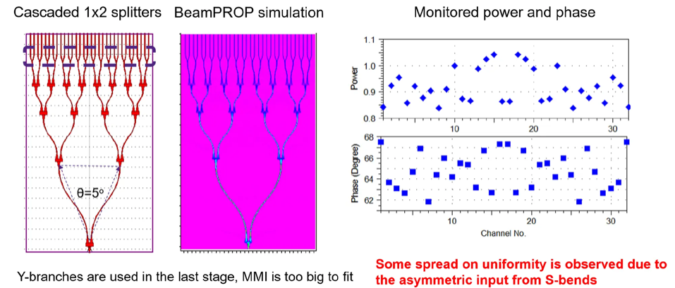
Cascaded 1×32 splitter: BeamPROP BPM
BPM is ideal for 1×2 splitters due to little backward reflection and suitability for slowly varying structures.
Thermo-optical phase shifter: BeamPROP BPM + Multiphysics Utility
BPM handles optical propagation, while the Multiphysics Utility computes temperature-dependent refractive index perturbations.
Emitter (grating antenna array): FullWAVE FDTD
FDTD (Finite Difference Time Domain) is required for omnidirectional light propagation and accurate grating coupler modelling.
This modular approach ensures each component is optimised using the most accurate and computationally efficient method available.
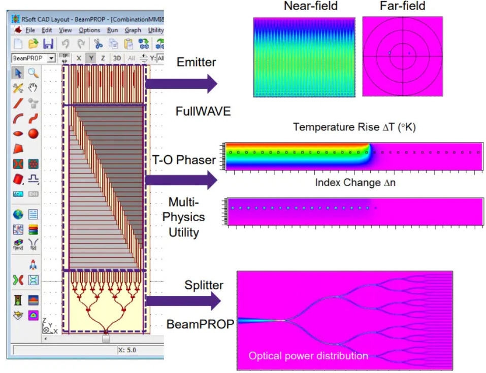
Step-by-Step Design of Individual Components
Power Splitter
A splitter tree is constructed using cascaded 1×2 splitters—either MMI or Y‑branch designs.
1×2 MMI splitters
- Low insertion loss (~0.3 dB)
- Robust to asymmetric input
- More complex to design
- Wavelength sensitive, limited bandwidth, polarisation dependent
Y‑branch splitters
- Simple geometry (two S‑bends)
- Broadband and polarisation independent
- Higher insertion loss (~2 dB)
- Less tolerant to asymmetric input
Both structures are well-suited to BeamPROP BPM, which solves one-way wave equations under assumptions of slow structural variation and monochromatic excitation.
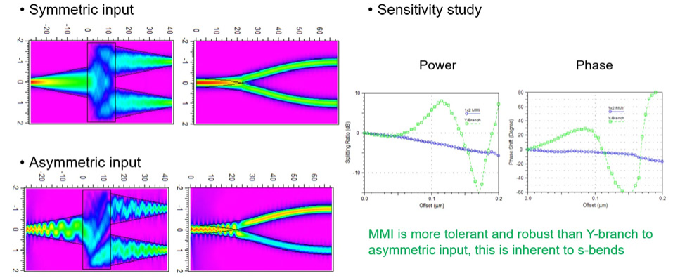
After optimising width and length using 2.5D (2D‑EIM) BPM, sensitivity analyses were performed for symmetric and asymmetric inputs. The final 1×32 splitter tree uses four levels of 1×2 MMIs, followed by a fifth level of Y‑branches where MMIs become too large to fit the remaining layout area.
Thermo-Optical Phase Shifter
Silicon’s strong thermal sensitivity (dn/dT = 0.00024/K) enables phase tuning by heating waveguide arrays. Unequal heating introduces phase delays between channels, steering the output beam.
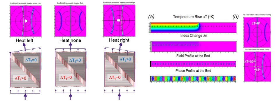
The workflow:
- The thermal diffusion equation was solved to obtain the temperature distribution.
- Temperature profile converted into refractive index perturbation.
- BPM simulates optical propagation to compute amplitude and phase at the output.
- Far‑field analysis reveals the resulting beam steering.
For a temperature change of ΔT = 50 °C, the phase difference between adjacent waveguides is 120°. BPM predicts a steering angle of 15°, matching the theoretical value:
Emitting Gratings
To efficiently outcouple light (orthogonally) with minimal divergence, the grating must be properly apodized. FDTD optimisation yields an optimal tapered-width grating profile, normalised to the grating length (Fig. 5).
The post Designing LIDAR on a Chip: A Multiphysics Simulation Workflow for Integrated Photonics appeared first on ELE Times.
Most of us started here
 | submitted by /u/hakh-ti-cxamen [link] [comments] |
Mastering EDA Tools: How India is Upskilling 85,000 Engineers for the Global Chip Race
The Government of India’s ‘Chips to Startups’ (C2S) programme, under the India Semiconductor Mission, has made tremendous progress, completing training for 85,000 engineers in semiconductor design over the past decade. Students have been trained in 315 academic institutions as part of the current chip design training programme.
Union Minister for Electronics and IT, Ashwini Vaishnaw, highlighted how the programme has provided students with an experience of using world-class EDA tools, such as Synopsys, Cadence, Renesas, AMD, Ansys, and Siemens. Using these tools, the students have experienced hands-on learning as needed when they step into the industry. So far, the ministry claims to have recorded more than 1.85 crore hours of EDA tool usage for chip design training.
The training under this programme comprises a holistic experience from design and fabrication to packaging and testing. The chips designed by students are tested at Mohali’s Semiconductor Laboratory. This allows them to understand the complete semiconductor development cycle.
Students from across the country are taking this training, and the government aims to expand this programme under the second edition of the India Semiconductor Mission by raising the number of affiliated institutions from 315 to 500.
As we expect the electronics industry to grow manifold in the coming years, the need for a skilled workforce is bound to rise exponentially, too. Hence, the upskilling and thorough training programme are important to keep India at the forefront of this global race.
By: Shreya Bansal | Sub-Editor
The post Mastering EDA Tools: How India is Upskilling 85,000 Engineers for the Global Chip Race appeared first on ELE Times.
Skyworks and MediaTek demo early 6G FR3 and PC1 RF front-end innovations at MWC
Analog IC longevity is an underappreciated reality

I recently saw an announcement from a major IC vendor, posted in September 2025, letting users know that “STMicroelectronics sets 20-year availability for popular automotive microcontrollers.” The news is that ST was committed to maintaining the cited parts for 20 years instead of their present 15-year assurance.
“Good for them” was my first thought, as that’s the right thig to do for both their OEM and actual vehicle customers. After all, with the average age of cars on the road in the United States approaching 15 years and with little sign of slowing down or even leveling off, that makes sense.
There are two presumed reasons for the longer lifetime. First, cars are built better; the “rust-bucket” and “fall apart” tendencies of many of those pre-1980/90 cars have greatly diminished due to better design, materials, paints, tests, and processes. Second, the cost of a new car is so high that even costly repairs make sense for many.
Ironically, those less reliable, mostly mechanical cars did have one major virtue: they were repairable then and can generally be repaired/restored even today. Many of their old parts are available via specialty sources either as “new old stock” (NOS) or slightly used. And those that can’t be sourced can be machined or 3D printed if the owner has time and resources.
The issue is not limited solely to cars; unavailable mechanical assemblies are a very different case than electronic ones. In 2022, a team at Verisurf was contracted by the U.S. Air Force to reverse engineer and recreate a 300-piece “throttle quadrant” from the E-3 Airborne Early Warning and Control System (AWACS), by disassembling an existing unit piece-by-piece (Figure 1). See “Reverse Engineering the Boeing E-3 Sentry’s Secondary Flight Controls”.

Figure 1 This throttle quadrant from an E-3 AWACS radar aircraft was recreated via precise piece-by-piece measurement and fabrication of each of its 300 pieces. Source: Verisurf
They used a combination of tools, including basic calipers, advanced metrology systems, CAD/CAM software, close-up photographs, and more to capture and then recreate this control unit-top tolerances of better than 0.005 inches.
For the computers-on-wheels electronics of today’s cars, it’s a very different reality. Will you be able to get an engine control module, or one of the other hundred or so MCU-based modules, even 15 years from now? I’m betting the answer is “no” or “very unlikely,” but we’ll have to wait and see how that story unfolds.
The issue of unavailable parts is not limited solely to automobiles, although that is the largest and most visible application. Unlike most consumer products, there are many areas where useful lives of 20, 30, and more years are expected. Among these are industrial applications, railways, mil/aero, critical infrastructure, and even some home systems such as HVACs.
The challenge of replacement parts and their relatively low volume is not being ignored, as the ST announcement shows. The U.S. Defense Microelectronics Agency (DMEA) has instituted an Advanced Technology Supplier Program V (ATSP V) with 13 companies that, among other objectives, includes approaches to developing and creating components in ultra-low volumes for repair and replacement.
What about “analog”?
With all these legitimate concerns about long-term component availability, there’s one interesting aspect. One fact does stand out: unlike digital ICs and processors, the analog world has a different mindset. Analog-circuit designers tend to stick with a component that they have used successfully, even if it’s a few years old and could easily be replaced by a nominally better part.
Ther are several reasons for this tactic. Once an analog part is in the signal chain meeting specs, there’s a reluctance to take change on a new part and design which may have unknown issues and idiosyncrasies. Factors such as parasitics, layout, and power-supply sensitivity (to cite a few) likely will affect design validation, in contrast to the field experience with the existing design.
There are classic analog parts that have been available for decades, and while not recommended for new designs, they are still available if needed for repair, replacement, or even a newer design. Even better, if they are not available, there is often a drop-in replacement with superior performance; this is especially the case for basic 8-pin op amps.
I can think of three “ancient” analog components as examples:
- The AD574 “complete” 12-bit A/D converter from Analog Devices, introduced in the 1978–1980, became the industry-standard ADC for microprocessor interfacing (Figure 2). It was notable for integrating a buried Zener reference clock and 3-state output buffers for direct 8/16-bit bus interfacing. While its die and process have been upgraded and it’s now available in other packages, you can still get it in the original 28-pin housing.

Figure 2 The 12-bit ADC was the first complete unit with “tight” specifications and is still offered 45 years after its initial release. Source: Analog Devices
- The INA133 instrumentation amplifier from Burr-Brown was introduced around 1998 (Burr-Brown was acquired by Texas Instruments in 2000), and it’s still offered in a variety of packages and grades by TI (Figure 3). Like AD574, it’s not recommended for new designs; you can see its top-tier specifications on page 40 of the 2000 Burr-Brown Product Selection Guide.

Figure 3 Burr-Brown’s INA133 instrumentation amplifier provided excellent performance with modest power requirements and has been continuously available since its introduction in 1998. Source: Texas Instruments
- Finally, we can’t look at the 555 timer-oscillator-multivibrator, a clear contender as one of the most classic components of all time and the longest-lived along with the 74 op amp (Figure 4). Devised by Hans Camenzind and marketed as an 8-pin DIP by Signetics in 1971, it’s still available in many versions, including duals and quads as well as CMOS variations. Despite its age, it’s often used to solve annoying timing and oscillator problems at low cost, and there are many “cookbooks” showing innovative ways in which it can be used.

Figure 4 It’s very likely that no IC has spawned more creative and clever design ideas and handbooks and solved as many circuit problems as the 555 timer-oscillator-multivibrator. Source: Wikipedia
There are others, of course, such as the 60-year-old 2N3905 or 2N2222 transistors—it doesn’t get more basic than that.
While many analog components have a long and viable life with their original or descendent vendors, there is even a solution for the many cases where that source does not want to manufacture or support that IC forever. Companies such as Rochester Electronics work out a formal arrangement and license to take over the rights, tooling, support, and test procedures for the parts. Users who need the part don’t need to consider grey-market or even counterfeit products; instead, they get ICs which are 100% legitimate but via a different supplier.
ST’s announcement is welcome, of course. I wish that more vendors would make that sort of commitment, difficult as it may be, or at least commit to licensing unwanted products to non-competing vendors. For now, if you want long-term continuity, stick with analog parts as much as possible.
Have you ever had to deal with repairing a product having electronic components that were no longer available, or even doing regular production on a long-lived product where you needed more than just a few? Did you find parts, or did you have to do a full redesign? How painful was that process?
Related Content
- Go offline, and crack open a design book
- 2N3904: Why use a 60-year-old transistor?
- Vacuum tubes are dead; long live vacuum tubes
- Thermal printers: should be obsolete, but still going strong
- Appliance schematic, wiring diagram bring troubleshooting joy
The post Analog IC longevity is an underappreciated reality appeared first on EDN.
From 10 to 1000 TOPS: Why Automotive Chips Need a New Architecture
Speaking at the Auto EV Tech Vision Summit 2025, Namrta Sharma, Technical Director at Aritrak Technologies, highlighted how chiplet architectures are emerging as a crucial enabler for the next generation of automotive semiconductors. As vehicles transition toward software-defined platforms, Sharma emphasized that semiconductor design must evolve to meet unprecedented computational demands while balancing cost, scalability, and time-to-market.
Setting the context, Sharma described the ongoing transformation in the automotive sector. “We should all agree that we are actually going through a metamorphosis,” she said, adding that the automotive industry is currently experiencing “a big transformation of the century.” Vehicles are no longer defined solely by mechanical and electrical components. Instead, the modern car is increasingly becoming a software-driven platform.
Computational Requirements at Rise in Automotives
“The car is no longer just mechanical and electrical,” Sharma noted. “The car is a software-defined vehicle. So, the role of the semiconductors in the car is also changing. It is no longer just adding to some features. It actually defines the car. It is the core intelligence of the car.” This shift is dramatically expanding the semiconductor requirements inside vehicles. Modern automotive electronics must support electrification, battery management, in-vehicle infotainment, constant connectivity, and advanced driver assistance systems (ADAS), while also laying the groundwork for autonomous driving.
Sharma highlighted how the computational requirements behind these capabilities have grown exponentially. “If you see the numbers for the compute, Level-2 ADAS required just 10 TOPS, which is 10 trillion operations per second, which was just a decade ago,” she explained. “But now the requirement is about 1,000 TOPS for full autonomy. So it is like a 100x gap.”
Limitations at Play
Meeting such performance requirements using conventional monolithic chip design is becoming increasingly difficult. Integrating CPUs, GPUs, communication circuits, and power management components into a single system-on-chip (SoC) results in extremely large semiconductor dies. However, manufacturing such large chips is constrained by physical and economic limits. “There is a limit. It is called the reticle limit,” Sharma explained. “That is the biggest size that we can manufacture in a foundry, and it is about 850 mm² as of now.”
Large monolithic chips also face yield challenges. A defect in even a small portion of a large die can render the entire chip unusable, leading to significant losses in manufacturing yield and rising costs. To address these issues, the semiconductor industry has increasingly turned to chiplet architectures. “The solution was simple,” Sharma said. “Just cut this big die into multiple dies. These are all small functioning blocks, and these are called chiplets.”
Chiplets: A Yield Optimisation Solution
By breaking down a large chip into smaller modular dies, chiplet architectures help overcome reticle limitations and improve yield. If a defect occurs, only the affected chiplet is discarded rather than the entire system. This modular approach has already gained traction in high-performance computing systems and is now finding relevance in automotive electronics.
Sharma also pointed out that chiplets enable a shift toward heterogeneous integration. Instead of manufacturing every component using the most advanced—and expensive—process node, different chiplets can be fabricated using technology nodes optimized for their specific functions. “For example, the CPU needs the highest compute, so it is in the latest technology node,” she explained. “But the other things, like sensors or memory engines, need not be.”
Chiplets Optimised Time to Market
Beyond cost and yield advantages, chiplets significantly improve time-to-market. Sharma emphasized that modular architectures allow semiconductor companies to reuse proven components and focus their efforts on product differentiation. “You need not design the whole chip, you need not design the whole SoC,” she said. “You can just design your differentiating chiplet.” This flexibility also allows manufacturers to scale systems quickly for different vehicle segments.
Performance levels can be adjusted simply by replacing or modifying individual chiplets, enabling rapid customization without redesigning the entire architecture. However, Sharma cautioned that the transition to chiplet-based systems introduces new challenges. With multiple chiplets integrated into a single package, design complexity shifts from the chip level to the system level. This requires advanced electronic design automation (EDA) tools capable of co-optimizing silicon, packaging, and interconnect technologies.
Testing & Standards
With this, testing and validation also become more complex. The success of chiplet integration depends on ensuring that each component integrated into the system is a “known good die.” As Sharma noted, this requires new testing methodologies and infrastructure capable of validating chiplets both individually and within the larger system.
Another key factor in the long-term success of chiplets is the development of industry-wide standards. Sharma highlighted the importance of emerging interconnect standards such as Universal Chiplet Interconnect Express (UCIe), which aim to enable interoperability between chiplets from different vendors. As the ecosystem evolves, Sharma believes collaboration across the semiconductor value chain will play a critical role. Foundries, design houses, EDA companies, substrate providers, and industry consortia are already working together to establish the standards and infrastructure needed to support chiplet-based systems.
Conclusion
Summarizing her key message, Sharma emphasized that chiplet architectures are not just about cost optimization. Instead, they represent a fundamental shift in how semiconductor systems are designed for rapidly evolving markets like automotive. “Chiplet heterogeneous integration provides not only the cost benefit,” she concluded, “it also provides the speed of execution—the speed to make changes fast and react to innovation.”
As automotive electronics continue to grow in complexity and performance requirements, chiplets may well become the architectural foundation enabling the next wave of innovation in software-defined vehicles.
The post From 10 to 1000 TOPS: Why Automotive Chips Need a New Architecture appeared first on ELE Times.
Evolution of Technology Calls for Continuous Upskilling of Industry Professionals: Arindam Lahiri, ASDC
As India’s mobility ecosystem undergoes rapid technological transformation, the importance of a skilled workforce has become more critical than ever. Electrification, connected vehicles, advanced electronics and digital technologies are reshaping the automotive landscape, creating both opportunities and challenges for the industry. In an exclusive conversation with ELETimes, Arindam Lahiri, CEO, ASDC, shares his insights on the opportunities and gaps that India possesses as it unravels the electronics revolution.
At the centre of this transformation is the Automotive Skills Development Council (ASDC), which plays a key role in developing industry-relevant skills and building a future-ready workforce. Established to align vocational training with the evolving needs of the automotive sector, ASDC works closely with industry bodies, government institutions and training partners to create a robust skill ecosystem.
The organisation is playing a key role in the evolution of India’s skill development ecosystem, emerging technological trends in the automotive sector and the initiatives being taken to prepare the next generation of professionals.
Here are the excerpts from the interview:
ELETimes: Could you briefly explain ASDC and its key objectives?
Arindam Lahiri: Automotive Skills Development Council is one of the 36 sector skill councils operating in India. Sector skill councils were created to bridge the gap between industry requirements and workforce capabilities by developing structured training frameworks aligned with specific industries. The council is promoted by three major industry associations: the Society of Indian Automobile Manufacturers (SIAM), the Automotive Component Manufacturers Association of India (ACMA), and the Federation of Automobile Dealers Associations (FADA). These organisations represent vehicle manufacturers, component manufacturers and dealerships respectively, ensuring that the entire automotive value chain is represented within ASDC’s governance framework. The council also works in close coordination with the Ministry of Skill Development and Entrepreneurship (MSDE). In addition, the Ministry of Heavy Industries (MHI) and the Ministry of Road Transport and Highways (MoRTH) serve as line ministries for the automotive sector.
More recently, ASDC has also become an affiliated awarding body under the National Council for Vocational Education and Training (NCVET), which is the apex regulator for skill education in India.
Our core objective is to create a national platform for skill development in the automotive sector. This involves developing industry-aligned training curricula, establishing rigorous assessment and certification processes and ensuring that training programmes meet global standards. Ultimately, skill development contributes to higher productivity within the industry, which leads to capital creation and economic growth. As businesses expand and reinvest their resources, this generates further employment opportunities. Another key focus area for us is integrating skill-based education within mainstream academic pathways, a vision that has been strongly reinforced by the National Education Policy (NEP 2020).
ELETimes: Over the last decade, how do you assess the progress made in India’s skill development ecosystem?
Arindam Lahiri: India has a long history of vocational training through institutions such as Industrial Training Institutes (ITIs), which were established soon after independence. These institutions have played an important role in producing skilled manpower for the engineering and manufacturing sectors.
However, the last decade has been particularly significant for the skill development landscape in India. With the launch of the national Skill India mission, the government brought skill development into mission mode. Under the leadership of the Prime Minister, multiple ministries, agencies and training institutions have come together under a common framework to strengthen vocational education.
This coordinated effort has created a strong momentum in the skill development ecosystem. At the same time, it is important to recognise that India is still in the early stages of building a fully mature vocational training system.
Within the automotive sector specifically, we see a large number of training initiatives being undertaken by vehicle manufacturers, component manufacturers and dealership networks. While these initiatives are valuable, there is significant scope to scale them further and create more structured pathways for skill development.
India’s automotive industry is globally competitive, with many international brands operating in the country. These companies maintain very high standards when it comes to workforce capabilities. One of the concerns often raised by industry is that graduates from engineering colleges, polytechnics and ITIs sometimes lack the practical skills required for immediate employment.
This is precisely where organisations like ASDC play a critical role. By working closely with industry, we identify skill gaps and develop training programmes that address those gaps. Our work includes curriculum development, training of trainers, development of learning content, candidate assessment and certification.
ELETimes: What initiatives is ASDC taking to ensure that its curriculum remains contemporary and globally relevant?
Arindam Lahiri: Our curriculum framework is built upon National Occupational Standards (NOS), which define the competencies required for specific job roles in the automotive sector. These standards form the foundation for developing qualification packs and training curricula.
The qualification framework and associated curricula are reviewed and approved by the National Skill Qualifications Committee under NCVET. This ensures that training programmes meet national standards and remain aligned with industry expectations.
At regular intervals, we undertake comprehensive reviews of our curriculum with the support of industry experts. These experts come from various segments of the automotive ecosystem, including manufacturing, servicing, supply chain and emerging technology domains. Their inputs help ensure that every qualification and training programme reflects real-world industry requirements.
In recent years, we have incorporated several emerging areas into our curriculum. These include electric mobility, Industry 4.0 technologies, sustainability practices, vehicle diagnostics and safety systems.
In addition to entry-level training programmes, we are increasingly focusing on upskilling and reskilling the existing workforce. As technology evolves, professionals who are already working in the industry must continuously update their skills to remain relevant.
Given the pace at which automotive technologies are advancing, curriculum development is not a one-time exercise. It is a continuous process that evolves alongside the industry.
ELETimes: Safety remains a major concern within the automotive ecosystem. How can the industry address safety challenges more effectively?
Arindam Lahiri: Safety is a critical aspect of the automotive sector, and it can broadly be viewed in two dimensions: industrial safety and road safety. Industrial safety relates to the safety of workers within manufacturing plants, workshops and service facilities. Employees involved in vehicle manufacturing, component production or vehicle servicing must follow strict safety protocols.
This aspect of safety has become even more important with the increasing electrification of vehicles. Electric vehicles operate on high-voltage systems, which can pose serious risks if proper safety procedures are not followed. Therefore, all our training programmes place significant emphasis on safety standards and best practices related to specific job roles.
The second dimension is road safety. Road safety involves both preventive measures and post-accident response mechanisms. Preventive measures include awareness programmes that educate people about responsible driving behaviour, traffic regulations and safe mobility practices.
ASDC has been actively working on awareness initiatives at colleges and educational institutions, where young drivers can be sensitised to road safety principles. In addition, we are exploring programmes related to first responder training so that individuals can respond effectively in the event of a road accident and help reduce fatalities.
ELETimes: What major technological trends do you expect to shape the automotive sector by 2026 and beyond?
Arindam Lahiri: Today’s vehicles are increasingly becoming sophisticated digital platforms. Modern automobiles contain a significant amount of electronic hardware and software systems, whether they are two-wheelers, passenger vehicles or commercial vehicles.
In recent years, the automotive industry has experienced supply challenges due to semiconductor shortages. While the situation has improved, the increasing reliance on electronic components highlights how deeply technology is embedded in modern vehicles.
Another major trend is the rapid advancement of software and computing capabilities within vehicles. Improvements in computing power, communication speeds and the adoption of 5G connectivity are enabling new forms of vehicle intelligence.
Connected vehicles are already becoming a reality. Many manufacturers can now monitor the performance and location of vehicles through remote systems. These systems can even predict maintenance requirements and detect potential issues before they escalate.
Technology is also transforming logistics and transportation. Road transport remains the backbone of India’s logistics sector, and digital tools are helping drivers, fleet owners, and logistics managers optimise operations and respond quickly to unexpected situations.
Electric mobility will continue to expand as battery technologies improve and charging infrastructure becomes more widespread. At the same time, research is progressing in areas such as hydrogen fuel cells and solar-powered mobility solutions.
For young professionals, this presents tremendous opportunities. Individuals who continuously upgrade their skills will find exciting career prospects in the automotive sector, both in India and globally.
ELETimes: If a student wants to pursue training in the automotive sector through ASDC, what is the process?
Arindam Lahiri: ASDC functions as an awarding body and does not directly operate training centres. Instead, we affiliate training institutions that deliver automotive skill programmes based on our curriculum framework.
Currently, more than 300 active training institutions across India are affiliated with ASDC. These institutions offer training in various automotive domains, ranging from vehicle servicing and diagnostics to emerging technologies.
Students who are interested in exploring career opportunities in the automotive sector can visit our dedicated career guidance platform at careerguide.asdc.org.in. This platform provides detailed information about different job roles, career pathways and training opportunities available within the automotive industry.
The platform also helps students understand how specific training programmes can lead to long-term career progression. It provides insights into training centres located across different regions of the country.
Students can also submit queries through the contact section of the ASDC website. Our team then guides them in selecting the appropriate training programme and identifying the nearest training centre offering that programme.
The post Evolution of Technology Calls for Continuous Upskilling of Industry Professionals: Arindam Lahiri, ASDC appeared first on ELE Times.
Complex System Design Is Key to Navigating the Evolving Tech Ecosystem: Sadaf Arif Siddiqui, Keysight
In a conversation with Kumar Harshit, Technology Correspondent, ELE Times, Sadaf Arif Siddiqui, Director Marketing, Keysight Technologies India, shares his perspective on the latest developments in India’s electronics and telecom sectors. He discusses how advanced design validation and other technologies are gaining traction in product development. Further, the conversation also touches upon India’s position in the upcoming 6G technology and how unprecedented challenges are awaiting us.
The conversation moves further to touch upon certain technical aspects of testing in aerospace and defense, along with the simultaneous growth being exhibited by various industries in India.
Here are the excerpts from the interview:
ELE Times: India is increasingly positioning itself as a design-led electronics ecosystem rather than a manufacturing-only hub. From your perspective, how is this shift changing the role of advanced design validation and emulation in development cycles?
S.A Siddiqui: This shift is reshaping how companies approach product development from the ground up. Today, the focus is firmly on establishing a fully integrated, end-to-end workflow that seamlessly spans the entire product lifecycle — from initial design and prototyping to rigorous validation and ultimately, full-scale manufacturing. In addition, strong policy support led by the government and a deep pool of engineering talent are collectively enabling the country to move beyond pure manufacturing and into high-value innovation and product ownership. A key example of this momentum is the government’s push toward self-reliance under initiatives such as Make in India. This effort is encouraging growth across sectors, including telecom, automotive, aerospace and defense, semiconductors, and electronics.
With these shifts, the role of design validation and emulation has become extremely critical. The technologies driving this innovation are only getting more complicated, and at the same time, there is growing pressure to launch products faster. In this environment, adopting advanced design validation as early as possible in the development cycle will give companies a competitive edge.
ELE Times: India has begun early conversations around 6G and non-terrestrial networks. What new testing challenges do these next-generation technologies introduce compared to 5G?
S.A Siddiqui India is positioning itself as an active contributor to 6G research and standardization, with several academic institutions, government research bodies, and the Ministry of Communications already engaged in exploratory programs to define India’s role in shaping 6G and non-terrestrial network (NTN) technologies.
5G primarily focused on enhanced mobile broadband, ultra-low latency, and high throughput. Whereas 6G and NTNs significantly expand the scope and are leveraging AI and communication to extend connectivity beyond terrestrial boundaries and into space through satellite networks. In terms of spectrum, 6G is projected to move beyond millimeter wave and into sub-terahertz (sub-THz) frequency bands.
This entirely changes the concept of testing in 6G. NTNs present challenges, the first being that satellite-based equipment, once deployed, is largely inaccessible. The technology also needs to operate in extremely harsh environments with temperature fluctuations and radiation. There are also challenges around frequency conditions, latency and doppler shifts. At the same time, energy efficiency is also a central pillar of 6G system design. Together, these requirements make 6G testing far more multidimensional than previous generations, demanding greater precision and accuracy under harsher conditions. As a result, over-the-air testing is growing in importance so developers can validate systems with the accuracy they need.
ELE Times: With vehicles becoming increasingly software-defined, how important is cross-domain validation — combining RF, digital, power electronics, and cybersecurity testing?
S.A Siddiqui: Cross-domain validation has become absolutely critical as the automotive industry evolves. Modern vehicles integrate a dense network of electronic control units (ECUs), sensors, high-speed digital interfaces, connectivity modules, and power electronics. This convergence of multiple domains means that validation can no longer occur in isolated silos. Instead, it must address the full system-level interaction between RF, digital, power, and software layers—particularly given the stringent safety, reliability, and regulatory requirements governing the automotive sector.
ELE Times: In aerospace and defence applications, testing is often mission-critical. How is the need for high-fidelity emulation and secure communications testing evolving in India?
S.A Siddiqui: Aerospace and Defense is one of the cornerstones of India’s ‘Make in India’ initiatives. This means all components should be developed in the country and fully integrated into the platform. As a result, validation and emulation are critical as every element needs to be deployed with extreme precision and accuracy. As India continues to push technology boundaries, testing needs are evolving, and this is a clear example. Every element, right from designing the first component through to the prototype and final product, must be tested in order to ensure precision. This also means testing under a wide set of conditions and environmental requirements.
ELE Times: India is one of the few markets where telecom, automotive, semiconductors, defence, and AI are all scaling simultaneously. How does this convergence influence the demand for advanced testing ecosystems?
S.A Siddiqui: India’s simultaneous scaling across multiple high-tech sectors creates a uniquely demanding environment for testing and validation. With the rapid development of technologies such as 5G/6G, artificial intelligence, semiconductors, quantum initiatives, and defence systems, the country is not only meeting domestic requirements but also positioning itself to compete on a global stage. This simultaneous growth across diverse sectors intensifies the need for integrated, high-performance testing ecosystems that can handle increasingly complex and interdependent technologies.
The convergence of RF, digital, software, and security components across these domains means that testing can no longer be confined to individual components or isolated subsystems. Instead, advanced testing must address full system-level interactions, integrating hardware, software, and cybersecurity layers to ensure reliable performance under real-world conditions. Dynamic, repetitive testing platforms are now essential, enabling engineers to validate interoperability, functionality, and robustness before deployment. Technologies such as digital twins are playing a transformative role in this context. By creating virtual replicas of systems, engineers can simulate and validate complex behaviors in the lab, reducing risk and accelerating development cycles before field testing.
ELE Times: Looking ahead 3–5 years, what will differentiate engineering organizations that succeed in complex system design from those that struggle?
S.A Siddiqui Over the next couple of years, the organizations that will excel in complex system design are those that can navigate a dynamic, rapidly evolving ecosystem while balancing immediate needs with future-facing innovation. Success will hinge on the ability to test as early as possible and throughout the entire development lifecycle – allowing organizations to improve speed to market, while still delivering on quality and meeting modern engineering challenges.
| Brief profile of the speaker:
Sadaf Arif Siddiqui is the Director of Marketing – India at Keysight Technologies, where he leads strategic marketing initiatives to support the company’s growth across telecommunications, automotive, aerospace & defense, and emerging technology segments. With over 23 years of experience in test, measurement, embedded systems, and technology solutions, Sadaf has driven customer engagement, industry partnerships, and market expansion throughout his career. He joined Keysight (formerly part of Agilent Technologies) in 2008 and has held multiple leadership roles spanning industry marketing, business development, and global program management. Sadaf holds a Bachelor’s degree in Electronics Engineering from Aligarh Muslim University and a Post Graduate Diploma in Business Management (Marketing) from Symbiosis Institute, Pune. |
The post Complex System Design Is Key to Navigating the Evolving Tech Ecosystem: Sadaf Arif Siddiqui, Keysight appeared first on ELE Times.
Elite level soldering
 | submitted by /u/YahudiKundakcisi [link] [comments] |
Building I2C-PPS. Part 5 - BOM
 | This is the next update on the programmable power supply project (you can find previous posts and more details in its umbrella repository condevtion/i2c-pps, while schematics itself is in condevtion/i2c-pps-hw). During the past week I managed to select exact market available components for the device and create detailed BOM. I need parts for 3 copies of the power supply - two sets to actually build devices and one on standby just in case. Honestly, I expected the BOM to be 3 times cheaper (or at least 2) but costs for hundred components quickly add up. In the first picture above (left chart) you can see average unit price of a part per its type with quite expected the BQ25758S controller being the most expensive thing. However, as the right chart shows total amount of capacitors easily gives them the lead in final cost, which is $108.88 (or $36.29 per set). For just one set the total is $48.99 making it almost buy two get one for free. The next picture shows quantities of parts per device and totals for 3 devices with additional components (marked green) per part type (total here is 393 for all 3 sets). The latest allows to reduce cost even further due to substantially lower prices on bigger quantities. Now, knowing exact parts and their footprints I can start designing PCB itself. [link] [comments] |
Weekly discussion, complaint, and rant thread
Open to anything, including discussions, complaints, and rants.
Sub rules do not apply, so don't bother reporting incivility, off-topic, or spam.
Reddit-wide rules do apply.
To see the newest posts, sort the comments by "new" (instead of "best" or "top").
[link] [comments]
My first two PCBs created while I try to teach myself electronics!
 | The first started as a way to test ADCs and parallel I/O, and I turned it into a toy oscilloscope using some software I wrote for my Raspberry Pi. I didn't really understand op-amp input bias current and so it doesn't really work properly with the probe in 10x mode. The offset is huge, but I now understand the mistake. I also used one more op-amp than I really needed, and could've gotten away with cheaper ones, but it works up to 50MS/s! The second board is a buffered variable-gain amplifier test with voltage-variable gain and bias. I fell down a rabbit hole w/oscilloscopes and am working on making an improved 2-channel one with modern components, so I broke out some of the front end into a test board and just finished building it. It's a miracle the QFN op-amp works, I was sure I'd bridge something underneath it. There's a subtle crucial mistake in the second design, all you need to know to spot it is that the second amp is an LMH6505. It somehow does partially function still! [link] [comments] |
Took apart this broken digital scale just for fun
 | submitted by /u/netsurfer79 [link] [comments] |
EEVblog 1738 - Solar Freakin' Roadways NEW FUNDING!
Risk assessment in the workplace

Risks come in more than one form. There are risks that arise from science and technology, and there are risks that arise from human motivations, which are not always of an obvious sort. This is about the latter.
I had a client company that was owned by a husband and wife for whom I had once solved a power supply thermal runaway problem. I had measured temperature rise versus time and temperature fall versus time, and of course, the two were not exactly the same. Their difference was quite pronounced when I first looked at the issue, but they were almost identical to each other after I had solved their problem. If you’re curious about that, please see the How2Power article here.
A couple of years went by, and I got a call from that same company about a different power supply that also seemed to have a thermal runaway problem. By then, sadly, the husband had passed away, and only the wife remained to run the business.
During the first time frame, the wife had displayed a hair-trigger temper. Any moment of uncertainty as events unfolded would result in a raging torrent from her, to which her husband would make great efforts to calm her down. I would hear lines like “It’s okay. It’s oh-kay! Please relax. Things are going well.” to which she would then go silent, but now she didn’t have anyone to give her any assurance when it was needed.
An employee who had been promoted to Chief Engineer was my new point of contact. I explained to him that I would examine the thermal rise and thermal fall traits of this new power supply to see if indeed the same situation pertained as it did in the first case or not.
“There’s no need for that. I’ve already made those measurements.” He handed me a sheet of paper with columns of numbers, purportedly the data I had planned to acquire. That night, I examined those numbers and discovered that if you plotted the thermal rise and inverted a plot of the thermal fall, the two curves precisely lined up and were EXACTLY the same!! There was absolutely zero difference. They were totally spot on, no ifs, ands, buts, hows, whys, or wherefores, exactly the same, which meant that the rising and falling curves given to me were not the results of actual testing. They were false.
Confronted with a Chief Engineer whom I then knew to be dishonest and confronted with the woman whom I knew to be extremely volatile and prone to bursts of rage, I assessed the risk of dealing with it all to be unacceptable.
I made up some excuse (I don’t remember what it was) and declined to offer my services.
John Dunn is an electronics consultant and a graduate of The Polytechnic Institute of Brooklyn (BSEE) and of New York University (MSEE).
Related Content
The post Risk assessment in the workplace appeared first on EDN.
New LX4580 – Highly Integrated 24‑Channel Mixed‑Signal IC for Aviation & Defence Actuation Systems
The post New LX4580 – Highly Integrated 24‑Channel Mixed‑Signal IC for Aviation & Defence Actuation Systems appeared first on ELE Times.
Last-level cache has become a critical SoC design element

As AI workloads extend across nearly every technology sector, systems must move more data, use memory more efficiently, and respond more predictably than traditional design methodologies allow. These pressures are exposing limitations in conventional system-on-chip (SoC) architectures as compute becomes increasingly heterogeneous and traffic patterns become more complex.
Modern SoCs integrate CPUs, GPUs, NPUs, and specialized accelerators that must operate concurrently, placing unprecedented strain on memory hierarchies and interconnects. To Keep processing units fully utilized requires high-bandwidth, low-latency access to data, making the memory hierarchy as critical to overall system effectiveness as raw performance.
On-chip interconnects move data quickly and predictably, but once requests reach external memory, latency increases, and timing becomes less consistent. As more data accesses go off chip, the gap between compute throughput and data availability widens. In these conditions, processing engines stall while waiting for memory transactions to complete, creating data starvation.
The role of last-level cache
To mitigate this imbalance, SoC designers are increasingly turning to last-level cache (LLC). Positioned between external memory and internal subsystems, LLC stores frequently accessed data close to compute resources, allowing requests to be served with significantly lower latency.
Unlike static buffers, an LLC dynamically fetches and evicts cache lines based on runtime behavior without direct CPU intervention. When deployed effectively, this architectural layer delivers measurable benefits, including substantial reductions in external memory traffic and power consumption.
Simply including an LLC does not guarantee improved performance. Configuring the cache correctly is a complex task that must account for workload characteristics, compute-unit behavior, and real-time constraints. Poorly chosen parameters can waste area without meaningful gains, while under-provisioned configurations may fail to alleviate memory bottlenecks.
Architects must carefully determine cache capacity, the number of cache instances, and internal banking structures to support sufficient parallelism. Partitioning strategies must also be defined to ensure that individual IP blocks receive the bandwidth and predictability they require. While some settings can be adjusted later through software, foundational decisions on cache size, banking, and associativity must be finalized early in the development cycle.

The role of last-level cache is shown in successful designs. Source: Arteris
Factors influencing cache behavior
Banking configuration illustrates this trade-off clearly. Increasing the number of cache banks improves internal parallelism and throughput, but it also increases silicon area. Workloads with largely sequential access patterns may see limited benefit from aggressive banking.
In contrast, highly parallel workloads, especially those driven by AI accelerators or GPUs, require substantial internal concurrency to maintain utilization. Because these characteristics vary by application, banking decisions must be informed by realistic workload analysis during the architectural phase.
Cache capacity is just as important. A cache that is too small struggles to achieve acceptable hit rates, pushing excessive traffic to external memory. Conversely, oversizing the cache often yields diminishing returns relative to the additional area consumed. The optimal balance depends on actual runtime behavior rather than theoretical assumptions.
In practice, acceptable hit rates vary widely. Some systems can tolerate moderate miss rates if latency and power reductions outweigh the cost, while real-time applications demand consistently high hit rates to maintain deterministic behavior.
This variability underscores why no single LLC configuration is universally optimal. Mobile devices may require only a few megabytes of cache to balance power efficiency and responsiveness. At the same time, servers and HPC platforms often deploy tens or hundreds of megabytes to reduce DRAM pressure. Despite these differences, successful designs rely on a common principle in which cache parameters are derived from the workloads the system will actually execute.
Managing shared caches
Diversity in system demands further complicates how an LLC must be structured. Automotive chips built around concurrent vision processing and strict timing requirements operate under very different constraints than data-center platforms optimized for accelerator-heavy inference at scale. Even within a single chip, CPUs, accelerators, and I/O subsystems generate distinct access patterns with different latency sensitivities.
The LLC must accommodate all of them without allowing one workload to interfere with another’s real-time guarantees. This makes early understanding of system-level access behavior essential, since cache configuration otherwise becomes speculative at best.
Partitioning provides a powerful mechanism for preserving determinism in such environments. By allocating portions of cache capacity to specific clients, architects can prevent high-bandwidth workloads from starving latency-sensitive subsystems. This capability is particularly critical in environments that must meet strict timing guarantees. Partition sizes must be tuned carefully, as oversizing wastes area while undersizing risks violating latency requirements.
Configuring a last-level cache is ultimately a multidimensional challenge shaped by workload demands, compute topology, latency requirements, and silicon constraints. Achieving the right balance between performance, determinism, power, and area depends on understanding how an SoC behaves under real operating conditions.
To address this, SoC teams increasingly rely on system-level simulation using realistic data flow profiles generated by multiple on-chip request sources. This approach allows teams to evaluate cache behavior before key architectural decisions are finalized. It helps identify bottlenecks, validate cache sizing, and determine when isolation mechanisms such as partitioning are required to preserve real-time guarantees.
Arteris developed its CodaCache IP, which operates as a configurable last-level cache between on-chip initiators and different types of external memories such as DDR-DRAM, HBM and even NVM for execution in place (EIP) use cases. With CodaCache, architects can equip their SoC fabric with the optimal configuration to address intelligent, scalable, and automated data management in a wide range of applications.
Andre Bonnardot is product marketing manager at Arteris.
Related Content
- Understanding cache placement
- Optimizing for instruction caches
- How to Turbo Charge Your SoC’s CPU(s)
- Bringing SOT-MRAM Tech Closer to Cache Memory
- SoC design: When a network-on-chip meets cache coherency
The post Last-level cache has become a critical SoC design element appeared first on EDN.
Marktech adds 230nm and 265nm deep UV, 310nm UVB and 340nm UVA LEDs
Pages


![[link]](https://i.redd.it/aic0w477mzng1.jpeg)
![[link]](https://i.redd.it/1r4p6nm6itng1.jpeg)
![[link]](https://i.redd.it/v8e3k39ipjng1.jpeg)