
Новини світу мікро- та наноелектроніки
Nuvoton Releases High-Power Ultraviolet Laser Diode (379 nm, 1.0 W)
Nuvoton Technology announced the start of mass production of its high-power ultraviolet semiconductor laser (379 nm, 1.0 W) [1], which delivers industry-leading optical output in a 9.0 mm diameter CAN package (TO-9) [2]. This product achieves short wavelength, high output power, and long lifetime—three elements previously considered difficult for ultraviolet semiconductor lasers—through our proprietary device structure and advanced high-heat-dissipation packaging technology. As a result, it contributes to fine patterning and improved production throughput in maskless lithography [3] for advanced semiconductor packaging [4].
Achievements:
- Achieves 1.0 W-class optical output at 379 nm, contributing to fine patterning and improved production throughput in maskless lithography for advanced semiconductor packaging.
- Improves heat dissipation of ultraviolet semiconductor lasers through our proprietary device structure and packaging technology, suppressing device degradation from self-heat generation and ultraviolet light and contributing to the extended lifetime of optical equipment.
- Expands the lineup of mercury lamp replacement solutions [5], enhancing flexibility in product selection to suit different applications.
Features of New Product:
- Achieves 1.0 W-class optical output at 379 nm, contributing to fine patterning and improved production throughput in maskless lithography for advanced semiconductor packaging.
As demand grows for information processing capabilities driven by the evolution of artificial intelligence (AI), there is an increasing need for higher performance from semiconductors than ever before. On the other hand, as the miniaturisation of transistors approaches its physical and economic limits, semiconductor back-end package technologies and advanced semiconductor packaging, which allow for integration by arranging multiple semiconductor chips side by side or stacking them vertically, have been attracting attention.
In advanced semiconductor packaging, the mainstream method for forming wiring connections between multiple semiconductor chips has been exposure technology using the i-line (365 nm) of the mercury spectrum and photomasks (master masks of circuits). On the other hand, there has been growing interest in recent years in maskless lithography technology, which directly exposes (draws) wiring patterns based on design data without using photomasks.
This technology is considered to reduce the time and cost associated with the design and production of photomasks. Furthermore, because it is possible to directly imprint wiring patterns to match the surface shape of the target for drawing, alignment and correction are easier, and application to advanced semiconductor packages is currently under consideration.
As one of the key light sources in maskless lithography, semiconductor lasers have faced increasing demands for shorter wavelengths closer to the i-line (365 nm) and higher output, to enable finer wiring and improve equipment throughput. To meet these requirements, we have leveraged over 40 years of experience in laser design and manufacturing to develop and commercialise an ultraviolet semiconductor laser with a wavelength of 379 nm and an output of 1.0 W.
- Improves heat dissipation of ultraviolet semiconductor lasers through our proprietary device structure and packaging technology, suppressing device degradation from self-heat generation and ultraviolet light and contributing to the extended lifetime of optical equipment.
Ultraviolet semiconductor lasers generally suffer from significant heat generation caused by low wall-plug efficiency (WPE)[6], and a tendency for device degradation caused by ultraviolet light, making stable operation at high output levels above 1.0 W difficult to achieve. To address this, we took a dual approach by focusing on both a “device structure that enhances wall-plug efficiency (WPE)” and a “high thermal conduction package technology that effectively dissipates heat,” enabling us to develop a product that successfully combines short wavelength, high output, and long lifetime: a 1.0 W ultraviolet (379 nm) device. As a result, we are contributing to extending the lifetime of optical devices that utilise ultraviolet light.
・Device structure to enhance wall-plug efficiency
In addition to optimising the emission layer and optical guide layer, we have adopted a proprietary structure that precisely controls the doping profile. By reducing light absorption loss and operating voltage, this allows electrical energy to be converted into light more efficiently.
・High thermal conduction package technology that efficiently dissipates heat
In addition to adopting a submount made of high thermal conductivity materials, the package materials have been revised to reduce thermal resistance. As a result, rises in device temperature are suppressed, allowing for stable operation at high output.
- Expands the lineup of mercury lamp replacement solutions, enhancing flexibility in product selection to suit different applications.
This product has been newly added to our lineup of “semiconductor laser-based alternatives to mercury lamps,” providing customers with a new choice. With this addition, customers can flexibly select products according to application, installation environment, and required performance, thereby increasing the freedom of system design.
Details of this new product will be showcased at our booth at SPIE Photonics West 2026 in San Francisco, USA, and at OPIE’26 in Yokohama, Japan. We sincerely look forward to welcoming you.
Applications:
- Maskless lithography
・ Resin curing
・ Marking
・ 3D printing
・ Biomedical
・ Alternative light source for mercury lamps, etc.
Definitions:
[1] Ultraviolet semiconductor laser:
Our term is for a semiconductor laser that emits laser light with a peak wavelength of approximately 380 nm or less.
[2] TO-9 CAN:
CAN-type package with a diameter of 9.0 mm.
[3] Maskless lithography:
A technology that directly exposes photosensitive materials (resist) on a substrate based on design data without using a photomask and forms fine patterns. When using laser light, it is also referred to as Laser Direct Imaging (LDI).
[4] Advanced semiconductor packaging:
An implementation technology in which multiple semiconductor chips are densely integrated to optimise performance and power efficiency.
[5] Mercury lamp replacement solutions:
Nuvoton Technology’s lineup of semiconductor lasers is designed to replace the emission lines of mercury lamps: i-line (365 nm), h-line (405 nm), and g-line (436 nm). We propose the combined use of ultraviolet semiconductor lasers (379 nm), violet semiconductor lasers (402 nm), and indigo semiconductor lasers (420 nm).
[6] Wall-Plug Efficiency (WPE)
An indicator of the efficiency of converting electrical input into optical output. It is generally used to express the emission efficiency of semiconductor lasers.
The post Nuvoton Releases High-Power Ultraviolet Laser Diode (379 nm, 1.0 W) appeared first on ELE Times.
AI workloads demand smarter SoC interconnect design

Artificial intelligence (AI) is transforming the semiconductor industry from the inside out, redefining not only what chips can do but how they are created. This impacts designs from data centers to the edge, including endpoint devices such as autonomous driving, drones, gaming systems, robotics, and smart homes. As complexity pushes beyond the limits of conventional engineering, a new generation of automation is reshaping how systems come together.
Instead of manually placing every switch, buffer, and timing pipeline stage, engineers can now use automation algorithms to generate optimal network-on-chip (NoC) configurations directly from their design specifications. The result is faster integration and shorter wirelengths, driving lower power consumption and latency, reduced congestion and area, and a more predictable outcome.
Below are the key takeaways of this article about AI workload demands in chip design:
- AI workloads have made existing SoC interconnect design impractical.
- Intelligent automation applies engineering heuristics to generate and optimize NoC architectures.
- Physically aware algorithms enhance timing closure, reduce power consumption, and shorten design cycles.
- Network topology automation is enabling a new class of AI system-on-chips (SoCs).
Machine learning guides smarter design decisions
As SoCs become central to AI systems, spanning high-performance computing (HPC) to low-power devices, the scale of on-chip communication now exceeds what traditional methods can manage effectively. Integrating thousands of interconnect paths has created data-movement demands that make automation essential.
Engineering heuristics analyze SoC specifications, performance targets, and connectivity requirements to make design decisions. This automation optimizes the resulting interconnect for throughput and latency within the physical constraints of the device floorplan. While engineers still set objectives such as bandwidth limits and timing margins, the automation engine ensures the implementation meets those goals with optimized wirelengths, resulting in lower latency and power consumption and reduced area.
This shift marks a new phase in automation. Decades of learned engineering heuristics are now captured in algorithms that are designing silicon that enables AI itself. By automatically exploring thousands of variations, NoC automation determines optimal topology configurations that meet bandwidth goals within the physical constraints of the design. This front-end intelligence enables earlier architectural convergence and provides the stability needed to manage the growing complexity of SoCs for AI applications.
Accelerating design convergence
In practice, automation generates and refines interconnect topologies based on system-level performance goals, eliminating the need for laborious repeated manual engineering adjustments, as shown in Figure 1. These automation capabilities enable rapid exploration and convergence of multiple different design configurations, shortening NoC iteration times by up to 90%. The benefits compound as designs scale, allowing teams to evaluate more options within a fixed schedule.

Figure 1 Automation replaces manual NoC generation, reducing power and latency while improving bandwidth and efficiency. Source: Arteris
Equally important, automation improves predictability. Physically aware algorithms recognize layout constraints early, minimizing congestion and improving timing closure. Teams can focus on higher-level architectural trade-offs rather than debugging pipeline delays or routing conflicts late in the flow.
AI workloads place extraordinary stress on interconnects. Training and inference involve moving vast amounts of data between compute clusters and high-bandwidth memory, where even microseconds of delay can affect throughput. Automated topology optimization ensures traffic flow to maintain consistent operation under heavy loads.
Physical awareness drives efficiency
In 3-nm technologies and beyond, routing wire parasitics are a significant factor in energy use. Automated NoC generation incorporates placement and floorplan awareness, optimizing wirelength and minimizing congestion to improve overall power efficiency.
Physically guided synthesis accelerates final implementation, allowing designs to reach timing closure faster, as Figure 2 illustrates. This approach provides a crucial advantage as interconnects now account for a large share of total SoC power consumption.

Figure 2 Smart NoC automation optimizes wirelength, performance, and area, delivering faster topology generation and higher-capacity connectivity. Source: Arteris
The outcome is silicon optimized for both computation and data movement. Automation enables every signal to take the best route possible within physical and electrical limits, maximizing utilization and overall system performance.
Additionally, automation delivers measurable gains in AI architectures. For example, in data centers, automated interconnect optimization manages multi-terabit data flows among heterogeneous processors and high-bandwidth memory stacks.
At the edge, where latency and battery life are critical, automation enables SoCs to process data locally without relying on the cloud. Across both environments, interconnect fabric automation ensures that systems meet escalating computational demands while remaining within realistic power envelopes.
Automation in designing AI
Automation has become both the architect and the workload. Automated systems can be used to explore multiple design options, optimize for power and performance simultaneously, and reuse verified network templates across derivative products. These advances redefine productivity, allowing smaller engineering teams to deliver increasingly complex SoCs in less time.
By embedding intelligence into the design process, automation transforms the interconnect from a passive conduit into an active enabler of AI performance. The result is a new generation of optimized silicon, where the foundation of computing evolves in step with the intelligence it supports.
Automation has become indispensable for next-generation SoCs, where the pace of architectural change exceeds traditional design capacity. By combining data analysis, physical awareness, and adaptive heuristics, engineers can build systems that are faster, leaner, and more energy efficient. These qualities define the future of AI computing.
 Rick Bye is director of product management and marketing at Arteris, overseeing the FlexNoC family of non-coherent NoC IP products. Previously, he was a senior product manager at Arm, responsible for a demonstration SoC and compression IP. Rick has extensive product management and marketing experience in semiconductors and embedded software.
Special Section: AI Design
The post AI workloads demand smarter SoC interconnect design appeared first on EDN.
SST & UMC Release 28nm SuperFlash Gen 4 for Next-Gen Automotive Controllers
- Automotive Electronics Council (AEC) Q-100 Grade 1 qualified for operating temperatures of -40°C to +150°C (Tj)
- Read access time < 12.5ns
- 100K+ endurance cycles
- Data retention of > 10 years @ 125°C
- Only 1-bit ECC required
- Qualification of 32Mb macro at auto grade 1 conditions:
- Zero bit failures (no ECC applied)
- Peak yield reached 100%
The post SST & UMC Release 28nm SuperFlash Gen 4 for Next-Gen Automotive Controllers appeared first on ELE Times.
Plastic TVS devices meet MIL-grade requirements

Microchip’s JANPTX transient voltage suppressors (TVS) are among the first to achieve MIL-PRF-19500 qualification in a plastic package. With a working voltage range from 5 V to 175 V, the JANPTX family provides a lightweight, cost-effective alternative to conventional hermetic TVS devices while maintaining required military performance.

Rated to clamp transients up to 1.5 kW (10/1000 µs waveform) and featuring response times under 100 ps (internal testing), the devices protect sensitive electronics in aerospace and defense systems. These surface-mount, unidirectional TVS diodes mitigate voltage transients caused by lightning strikes, electrostatic discharge, and electrical surges.
JANPTX TVS devices safeguard airborne avionics, electrical systems, and other mission-critical applications where low voltage and high reliability are required. They protect against switching transients, RF-induced effects, EMP, and secondary lightning, meeting IEC61000-4-2, -4-4, and -4-5 standards.
Available now in production quantities, the JANPTX product line spans five device variants with multiple JAN-qualified ordering options. View the datasheet for full specifications and application information.
The post Plastic TVS devices meet MIL-grade requirements appeared first on EDN.
Snap-in capacitors handle higher voltages

Vishay has added 550‑V and 600‑V options to its 193 PUR‑SI line of miniature snap‑in aluminum electrolytic capacitors. According to the manufacturer, the capacitors deliver up to 30% higher ripple current than standard components of similar case sizes, along with a longer useful life.

Designers often connect three 400‑V to 450‑V capacitors in series, with voltage‑balancing resistors across each device, to handle DC bus voltages up to 1100 V. While effective, this approach increases design complexity and introduces potential failure points.
With voltage ratings up to 600 V, the 193 PUR‑SI family allows designers to handle DC bus voltages up to 1100 V using fewer capacitors. This eliminates the need for voltage‑balancing resistors, saving PCB space and reducing BOM costs. The additional voltage headroom also extends capacitor lifetimes and improves overall system reliability.
In addition to higher voltage ratings, the 193 PUR‑SI series provides robust performance and flexible configurations. The capacitors handle ripple currents up to 3.27 A and offer capacitance from 47 µF to 820 µF in 25 case sizes. A rated life of 5000 hours at +105°C enables up to 25 years of operation at +60°C.
Samples of the extended 193 PUR‑SI series capacitors can be ordered from catalog distributors in small quantities. Production quantities are currently available, with lead times of 18 weeks.
The post Snap-in capacitors handle higher voltages appeared first on EDN.
Low-power TMR switches boost magnetic sensitivity

Two omnipolar magnetic switches, the LF21173TMR and LF21177TMR from Littelfuse, combine tunneling magnetoresistance (TMR) and CMOS technologies in a compact LGA4 package. Compared with conventional Hall-effect switches, these TMR devices offer higher sensitivity and lower power consumption, making them useful for energy-efficient designs.

Operating from 1.8 V to 5.5 V while consuming just 160 nA, the LF21173TMR and LF21177TMR deliver typical sensitivities of 10 Gauss and 30 Gauss, respectively. This high magnetic sensitivity ensures reliable detection even with smaller magnets, enabling more compact product designs without sacrificing performance.
Unlike Hall-effect sensors, which rely on voltage generated by magnetic flux, TMR sensors detect resistance changes in magnetic tunnel junctions. This approach produces stronger signal outputs at lower current levels, allowing engineers to create smaller, longer-lasting, and more energy-efficient devices—extending battery life in portable electronics.
Samples of the LF21173TMR and LF21177TMR are available through authorized Littelfuse distributors.
The post Low-power TMR switches boost magnetic sensitivity appeared first on EDN.
Samsung achieves live single-server vRAN

Samsung has completed the industry’s first commercial call using its virtualized RAN (vRAN) on a Tier 1 U.S. operator’s live network. Powered by an Intel Xeon 6 SoC with up to 72 cores, the vRAN is designed to accelerate AI-native, 6G-ready networks, delivering higher performance and improved efficiency. This milestone builds on Samsung’s 2024 achievement of completing an end-to-end call in a lab environment with the same Xeon 6 SoC.

The vRAN ran on a single HPE commercial off-the-shelf server using a Wind River cloud platform, consolidating multiple network functions—mobile core, radio access, transport, and security—onto one server. With Intel Advanced Matrix Extensions (AMX) and vRAN Boost, the deployment delivered improved AI processing, memory bandwidth, and energy efficiency compared with previous generations. This setup demonstrates the feasibility of single-server vRAN deployments for live, commercial networks.
By enabling consolidation of RAN and AI workloads on fewer servers, operators can simplify site management, reduce power consumption, and lower capital and operational expenditures. The approach supports software-driven, flexible architectures that are AI-ready and scalable, helping networks move toward automation and preparing them for next-generation 6G capabilities.
Read the complete press release here.
The post Samsung achieves live single-server vRAN appeared first on EDN.
Controllers simplify USB-C dual-role power delivery

Diodes’ AP53781 and AP53782 are USB Type-C Power Delivery 3.1 dual-role power (DRP) controllers for battery-powered systems. They manage USB PD power negotiation for USB-C ports that can operate as either a power sink or power source, supporting Standard Power Range (SPR) profiles up to 21 V and Extended Power Range with Adjustable Voltage Supply (EPR/AVS) up to 28 V.

Both controllers include built-in firmware for automatic USB PD 3.1 negotiation, enabling sink operation when connected to a PD-compliant charger and source operation when powering a connected USB-C device. In dead-battery mode, the controllers force sink operation until external VBUS is detected. Typical applications for dual-role USB-C ports include power banks, power tools, e-bikes, and portable displays.
The AP53781 features resistor-configurable, preloaded PDO/RDO profiles that enable fixed source and sink operation without a host MCU. In contrast, the AP53782 adds an I²C interface that allows a host MCU to dynamically configure power profiles and implement more advanced power-management functions.
The AP53781 and AP53782 are priced at $0.57 and $0.59, respectively, in 1000-unit quantities.
The post Controllers simplify USB-C dual-role power delivery appeared first on EDN.
EIB backs Europe’s first gallium production investment with €90m for METLEN
I made an open source CAM tool for easy PCB fabrication. Hope you guys find it useful.
Hi everyone, I started making an isolation routing CAM tool for myself cause I disliked the alternatives and things snowballed a bit.
https://github.com/RicardoJCMarques/EasyTrace5000
It's 100% online, client-side, open-source and free to use. Although I am looking for sponsors to help with some development costs. Especially hardware partners so I can start working on a dedicated fiber/UV laser pipeline.
It uses Clipper2 WASM for boolean operations and then a custom algorithm reconstructs curves from the original geometry (it's not arc fitting). Meaning the output g-code can have G2/G3 commands. (Mostly G2 because of cut direction but that's another story.)
Post-processors need more testing but grbl should be safe and usable. Use it with a bit of caution. The others try them with extra caution, especially Roland RML. I've tested as much as I can although I only have a cheap grbl machine. Soon I may go somewhere that has a Roland cnc.
Work-flow is simple, add files and select them on the left nav-tree to expose parameters then it should be straight forward. Origin/rotation and machine stuff are exposed on tool loading but collapse to the top right.
Documentation is an AI placeholder although it should do the trick for a while. I'll write something from scratch soonish.
Let me know what you guys think. I'd love to get as much feedback as possible at this point. Both what's good and what's bad and what's uterly broken so I can focus where I should. The issue tracker on the repo is also available.
[link] [comments]
Sonic excellence: Music (and other audio sources) in the office, part 2

Last time, our engineer covered the audio equipment stacks on either side of his laptop. But what do they connect to, and what connects to them? Read on for the remaining details.
I wrapped up the initial entry in this two-part series with the following prose:
So far, we’ve covered the two stacks’ details. But what does each’s remaining S/PDIF DAC input connect to? And to what do they connect on the output end, and how? Stay tuned for part 2 to come next for the answers to these questions, along with other coverage topics.
“Next” is now. Here again is the unbalanced (i.e., single-ended) connection setup to the right of my laptop:

And here’s its higher-end balanced counterpart to the left:

As was the case last time in describing both stacks, I’m going to begin this explanation of the remainder of the audio playback chain at the end (with the speakers and power amplifiers), working my way from there back through the stacks to the beginning (the other audio sources). I’ll start by sharing another photo, of the right-channel speaker and associated hardware, that regular readers have already seen, first as a reference in the comment section and subsequently as an embedded image within the main writeup:

Here’s the relevant excerpt from the first post’s comments section:
I thought I’d share one initial photo from my ears-on testing of the Schiit Rekkr. The speakers are located 3.5 feet away from me and tilted slightly downward (for tweeter-positioning alignment with my ears) and toward the center listening position. As mentioned in the writeup, they’re Audioengine’s P4 Passives. And the stands are from Monoprice. As you’ll see, I’m currently running two Rekkrs, each one in monoblock mode.
Here’s a “stock” photo of the speakers:

Along with a “stock” photo of one of the stands:

At this point, you might be asking yourself a question along the lines of the following: “He’s got two audio equipment stacks…how does he drive a single set of speakers from both of them?” The answer, dear readers, is at the bottom of the left speaker, which you haven’t yet seen:

That’s another Schiit Sys passive switch, the same as the one in the earlier right-of-laptop stack albeit a different color, and this time underneath the Rekkr power amplifier at that location:


The rear-panel RCA outputs of the Schiit Vali 2++ (PDF) tube-based headphone amplifier at the top of the right-side stack:


and the 3.5 mm (“1/8 in.”) single-ended headphone mini-jack at the front of the Drop + THX AAA 789 amplifier at the top of the left-side stack:


Both route to it, and I as-desired use the Sys to switch between them, with the Sys outputs then connected to the Rekkrs. Well…sorta. There’s one more link in the chain between the Sys and the Rekkrs that I haven’t yet mentioned.
Wireless connectivityThe Audioengine P4 Passives deliver great sound, especially considering their compact size, but their front ported design can’t completely counterbalance the fact that the woofers are only 4” in diameter. Therefore explaining the other Audioengine speaker in the room, the company’s compact (albeit perfect for the office’s diminutive dimensions) P6 subwoofer based on a 6″ long throw front-firing woofer along with an integrated 140W RMS Class D amplifier:


And since I’d purchased the wireless variant of the P6, Audiosource had also bundled its W3 wireless transmitter and receiver kit with the subwoofer:


The Sys left and right outputs both get split, with each output then routing in parallel both to the relevant Rekkr and to the W3 transmitter input’s correct channel. The receiver is roughly 12 feet away, to my left at the end of the room and connected to (and powered by) the back panel of the W6 subwoofer.
The transmitter and receiver aren’t even close to being line-of-sight aligned with each other, but the 2.4 GHz ISM band link between them still does a near-perfect job of managing connectivity. The only time I encounter dropouts, and then only briefly, is when a water-rich object (i.e., one of the humans, or our dog) moves in-between them. And although I was initially worried that the active W3 transmissions might destructively interfere with Bluetooth and/or Wi-Fi, I’m happy to report I haven’t experienced any degradation here, either.
Audio source diversityThat covers one end of the chain: now, what about the non-computer audio sources? There’s only one device, actually, shared between the two stacks, although its functional flexibility enables both native and connected content source diversity. And you’ve already heard about it, too; it’s the Bluesound NODE N130 that I initially mentioned at the beginning of 2023:


It integrates support for a diversity of streaming music services; although I could alternatively “tune in” to this same content via a connected computer, it’s nice not to have to bother booting one up if all I want to do is relax and audition some tunes. Integrated Bluetooth connectivity mates it easily with my Audio-Technica AT-LP60XBT turntable:

And a wiring harness mates it with the analog audio output of my ancient large-screen LCD computer monitor, acting as a pseudo TV in combination with my Xbox 360 (implementing Media Center Extender functionality) and Google Chromecast with Google TV.

The Bluesound NODE N130 has three audio output options, which conveniently operate concurrently: analog and both optical and coaxial (RCA) S/PDIF. The first goes to my Yamaha SR-C20A sound bar, the successor to the ill-fated Hisense unit I groused about back in mid-2023:

And the other two route to the Drop + Grace Design Standard DAC Balanced at the bottom of the left-side stack (optical S/PDIF):


and the Schiit Modi Multibit 1 DAC at the bottom of the right-side stack (coaxial RCA S/PDIF):


The multi-stack connectivity repetition is somewhat superfluous, but since it was a feasible possibility, I figured, why not? That said, I can always redirect one of the stack’s DACs to some other digitally tethered to-be-acquired widget in the future. And as mentioned in part 1 of this series, the Modi Multibit 1’s other (optical) S/PDIF input remains unpopulated right now, too.
That’s all (at least for now), folksAfter a two-post series spanning 2,000+ words, there’s my combo home office and “man cave” audio setup in (much more than) a nutshell. Feedback is, as always, welcomed in the comments!
—Brian Dipert is the Principal at Sierra Media and a former technical editor at EDN Magazine, where he still regularly contributes as a freelancer.
Related Content
- Sonic excellence: Music (and other audio sources) in the office, part 1
- Audio amplifiers: How much power (and at what tradeoffs) is really required?
- Audio Amplifiers from Class A, B, D to T
- Class D audio power amplifiers: Adding punch to your sound design
- Audio amplifier selection in hearable designs
- The Schiit Modi Multibit: A little wiggling ensures this DAC won’t quit
The post Sonic excellence: Music (and other audio sources) in the office, part 2 appeared first on EDN.
“The role of distributors is rapidly evolving as India’s electronics manufacturing sector expands,” says Dr. Raphael Salmi of Arrow Electronics
| Dr. Raphael Salmi is the president of Arrow Electronics’ South Asia, Korea, and Japan components business. He is responsible for overseeing the teams supporting Indonesia, Malaysia, the Philippines, Singapore, Thailand, Vietnam, India, Korea, Japan, Australia, and New Zealand.
With over 19 years at Arrow, Raphael brings extensive experience overseeing various businesses in the Americas and EMEA, focused on driving and achieving growth, innovation, and performance on a global scale. |
As the electronic industry moves past 2025, it advances with significant strides in electronic design systems, encompassing power efficiency, thermal management, and materials. Also, for India, 2025 remained a high-growth year in electronics, wherein the exports of the same grew sixfold from ₹1.9 lakh crore to ₹11.3 lakh crore in a decade. But all this can be sustained and progressed further only through a strong backing in R&D capabilities, as well as exceptional engineering capabilities and resources. In an exclusive conversation with ELE Times, Dr. Raphael Salmi, President – South Asia, Korea, and Japan Components, Arrow Electronics & Bhartendu Mishra, Managing Director – India, Arrow Electronics, discuss these issues in some detail.
Dr. Raphael Salmi notes, “ The role of distributors is rapidly evolving as technology accelerates and India’s electronics manufacturing sector expands,” while he underlines the role of component distributors in India’s dynamic electronics landscape.
Challenges faced by Design Engineers in India
Apart from the core challenges of supply chain and reliable sourcing being evidently face-to-face in the electronics design industry, Dr. Salmi points towards a growing trend in the Indian landscape. He says,” There is an increasing demand for end-to-end engineering capabilities to accelerate innovation and achieve faster time-to-market.”
He adds that his company addresses these challenges by leveraging its extensive technology portfolio, deep engineering expertise, and comprehensive supply chain services coupled with a robust trade compliance program, aiming to empower innovation & resilience in India’s rapidly growing market.
Distributors’ Role – As India Chases the Electronics Dream
As India grows its electronics footprint, the role of electronics distributors is obvious to transform as it forms the very core of Research & development in the sector. To this, Dr. Salmi says, “The role of distributors is rapidly evolving as technology accelerates and India’s electronics manufacturing sector expands”.
Arrow does this by allowing its customers to outsource portions of their supply chain or specific elements of their bill of materials to it, while the companies can focus on research, development, and go-to-market strategies. This allows for enhanced efficiency and flexibility in the entire landscape. For Arrow’s role in India’s dynamically growing electronics landscape, Dr. Salmi says, “ For Arrow, India serves as a key hub for engineering, integration, and supply chain services. . We are committed to serving the Indian market by leveraging our extensive technology portfolio, engineering expertise, and supply chain capabilities to help customers innovate
faster and scale efficiently, and capture these burgeoning opportunities”.
Design Centre in India
Arrow’s recently inaugurated Arrow Engineering Solutions Center in Bangalore is a testament to its commitment to serve and rope in the Indian design engineering talent into the latest innovations in the sector. Bhartendu says, “ The center helps bridge gaps in local engineering capabilities and accelerates adoption of next-generation technologies, such as AIoT, edge computing, and intelligent sensing—reinforcing Arrow’s commitment to innovation and customer success.”
It enables world-class engineering support and advanced technology resources for sectors such as industrial, automotive, transportation, energy management, aerospace, and defense, he adds.
Arrow’s Beyond Components Approach
Arrow’s approach beyond components says a lot about its efforts to support and empower the design engineers. Beyond distribution, it enables supply chain management, engineering design, and integration services, allowing it to act as an extension of OEMs and suppliers’ product development teams.
Bhartendu Mishra, Managing Director – India, Arrow Electronics, says, “ Our robust compliance framework, global reach, and ability to deliver innovative solutions make Arrow a trusted partner for design engineers seeking reliability, expertise, and comprehensive support”.
Looking Ahead
Concluding the discussion, Dr. Salmi highlights Arrow Electronics’ commitment to empowering customers and suppliers across India and Asia-Pacific through its platform-based, data-driven model. The company is expanding value-added services in design engineering, integration, and supply chain management to help customers innovate faster and reach the market sooner. Continued investments in digital platforms will improve real-time access to inventory, pricing, and design resources, while a strong vertical focus on energy management, robotics, AIoT, and e-mobility will anchor Arrow’s growth strategy in the region.
| India’s semiconductor ambitions are backed by initiatives like the ₹76,000 crore ISM and the ₹1,000 crore DLI scheme, which focuses on fostering a strong design ecosystem. A critical part of this effort is ensuring design engineers get timely access to quality components.
To highlight how distributors are enabling this, we present our exclusive series — “Powering the Chip Chain” — featuring conversations with key industry players. |
The post “The role of distributors is rapidly evolving as India’s electronics manufacturing sector expands,” says Dr. Raphael Salmi of Arrow Electronics appeared first on ELE Times.
Global AI Spending to Reach $2.5 Trillion in 2026, Predicts Gartner
Gartner, a business and technology insights company forcasts the global AI spending to rise to $ 2.52 trillion this year through a 44% increase year-over-year.
“AI adoption is fundamentally shaped by the readiness of both human capital and organisational processes, not merely by financial investment,” said John-David Lovelock, Distinguished VP Analyst at Gartner. Organisations with greater experiential maturity and self-awareness are increasingly prioritising proven outcomes over speculative potential.
“Because AI is in the Trough of Disillusionment throughout 2026, it will most often be sold to enterprises by their incumbent software provider rather than bought as part of a new moonshot project,” said Lovelock. “The improved predictability of ROI must occur before AI can truly be scaled up by the enterprise.”
Building AI foundations alone will drive a 49% increase in spending on AI-optimised servers, representing 17% of total AI spending (see Table 1). AI infrastructure will also add $401 billion in spending as a result of technology providers building out AI foundations.
Table 1: Worldwide AI Spending by Market, 2025-2027 (Millions of U.S. Dollars)
| Market | 2025 | 2026 | 2027 |
| AI Services | 439,438 | 588,645 | 761,042 |
| AI Cybersecurity | 25,920 | 51,347 | 85,997 |
| AI Software | 283,136 | 452,458 | 636,146 |
| AI Models | 14,416 | 26,380 | 43,449 |
| AI Platforms for Data Science and Machine Learning | 21,868 | 31,120 | 44,482 |
| AI Application Development Platforms | 6,587 | 8,416 | 10,922 |
| AI Data | 827 | 3,119 | 6,440 |
| AI Infrastructure | 964,960 | 1,366,360 | 1,748,212 |
| Total AI Spending | 1,757,152 | 2,527,845 | 3,336,690 |
Source: Gartner (January 2026)
The post Global AI Spending to Reach $2.5 Trillion in 2026, Predicts Gartner appeared first on ELE Times.
SemiLEDs revenue falls quarter-to-quarter, but doubles year-on-year
Industry 5.0 in Practice: Collaborative, Connected, and Conscious Manufacturing
As the world transitions towards Industry 5.0, the notion of smart factories is no science fiction. The concept of smart manufacturing revolves around collecting, analysing, and using data from multiple sources to automate and optimise processes. India’s Smart factory market is projected to grow at a 14.3% CAGR (2025-30) to reach USD 15.6 billion by 2026. Among the various industries, the electronics and semiconductors sector is expected to be the fastest-growing in the adoption of Industry 5.0. The concept of Industry 5.0 thrives on three basic pillars– human-centricity and collaboration, sustainability, and resilience.
The game of smart manufacturing is all about the usage of data. The one who has the most holistic variety of data is bound to excel in the adoption and implementation of smart factories. From advanced automation, using AI, harnessing updated IoT technology, and big data analytics, the real deal of manufacturing lies in how well data can be used. Apart from these, the biggest innovations in Industry 5.0 are the use of ‘cobots’, or as one would call them, collaborative robots. Among the various technological advancements, the ‘Human-Machine Interface’ (HMI) is projected to be the fastest-growing technology segment in the Indian Smart Factory market.
Shifting from Industry 4.0
Industry 4.0 focused largely on technological advancement to boost the pace of production and its efficiency, and it was often said that this advancement of technology would eventually replace the human workforce. However, the trend changes with the adoption of Industry 5.0.
So, the idea now is that digitalisation will not make humans in industrial manufacturing obsolete; instead, it will integrate smart automation, systems, and devices in the workplace to promote cooperation and collaboration between humans and machines.
Technology in Smart Manufacturing
Core technologies under the smart manufacturing set-up of Industry 5.0 are said to work on edge-computing, cybersecurity measures, cloud-computing, Artificial Intelligence and Machine Learning, and big data analytics.
Edge and cloud computing in Industry 5.0 smart manufacturing offer real-time responsiveness (Edge), enhanced human-cobot collaboration, greater flexibility for mass customization, improved security/privacy, reduced costs/bandwidth, and powerful predictive analytics, with the cloud handling heavy storage/complex AI while the edge provides speed and reliability for immediate action, enabling personalized, sustainable, and efficient production.
Man + Machine Middleware
The contemporary concept of smart factories is no longer just automation through machines. Today, it is all about the ‘coexistence’ of humans and machines, and that is exactly what everyone is focused on!

While there is a buzz about AI taking over human jobs in the coming future, the real deal is that humans are central to manufacturing; however, the role of the human workforce will shift from handling repetitive and laborious tasks to indulging in customisation and creativity.
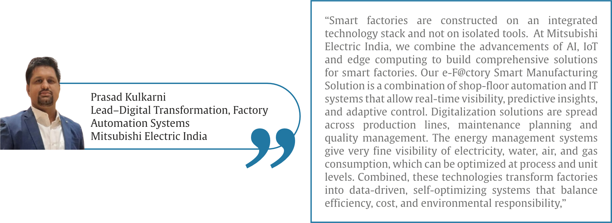
“The integration of AI and machine learning enables better human-machine collaboration where technology adapts to human needs on a real-time basis. IoT turns equipment into context-aware responsive assets. Digital twins enable engineers and operators to experiment in the virtual world, which is less risky and less cognitively demanding than the shop floor. Complex data is converted into easy-to-use visual and tactile interfaces with advanced HMIs, which can be used to make decisions faster and more safely,” reflects Prasad Kulkarni, Lead–Digital Transformation, Factory Automation Systems, Mitsubishi Electric India.
“Co” in Cobot
Imagine a workspace where a technician is hand-soldering a custom prototype while, just inches away, a robotic arm is flawlessly placing components the size of a grain of salt with 0.01mm precision. Meet your new favourite bench-mate. It doesn’t take coffee breaks, it never gets a “Monday morning” headache, and it can hold a PCB steady for hours without a single tremor. Cobots are the literal “Helping Hands” of Industry 5.0, filling the gap between rigid automation and the high-touch craftsmanship that modern electronics manufacturing requires.
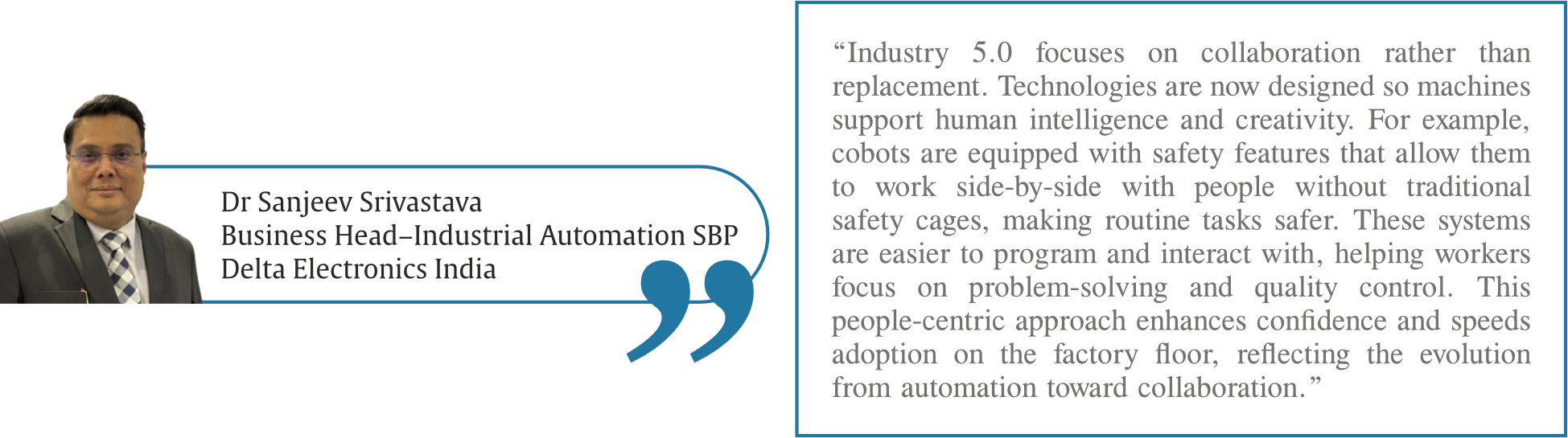
“Cobots are designed with safety and human collaboration in mind. They include sensors and control systems that detect human proximity and can instantly slow or stop motion to prevent accidents. Their flexibility and ease of programming make them suitable for varied tasks such as assembly, material handling, and packaging. These features help reduce worker fatigue and ergonomic risk while maintaining process consistency. When used properly, cobots enhance productivity and workplace safety, enabling humans to focus on tasks that require judgment and creativity,” underscores Dr Sanjeev Srivastava, Business Head–Industrial Automation SBP, Delta Electronics India.
Throwing light on the working mechanism of cobots, Prasad Kulkarni, Lead–Digital Transformation, Factory Automation Systems, Mitsubishi Electric India, detailed, “Cobots are designed with safety, flexibility, and ergonomics as core principles. They are specifically engineered to work safely alongside human operators. This is achieved through built-in safety mechanisms such as force and torque limitation, advanced vision systems, proximity sensing, and real-time feedback, which enable immediate response to human presence. From an efficiency standpoint, cobots deliver high consistency and precision in tasks such as calibration, complex assembly, inspection, sealant application, etc.”
Adoption and Challenges
The complete adoption of smart manufacturing under Industry 5.0 is still a work in progress, but “Adoption of Industry 5.0–aligned technologies is steadily increasing, particularly among organisations seeking flexibility, scalability, and workforce sustainability. While early adoption has been led by larger enterprises, interest from mid-sized manufacturers is also growing. In the long term, this trend will result in more resilient supply chains, faster response to market changes, and a workforce that is better supported by intelligent automation,” confirms Prateek Jain, COO and Co- founder of Addverb.
The International Federation of Robotics predicts that 35% of worldwide manufacturers will implement Industry 5.0 technologies (such as cobots) over the next decade to unite automated systems with human capabilities.
The shift is not expected to take too long; however, there are certain challenges that one may face in the course of time. “One challenge is integrating advanced automation with existing equipment and processes without overwhelming operators. Smart solutions must be powerful yet intuitive. Connectivity and cybersecurity are also critical as more systems communicate across networks. Additionally, helping the workforce upskill and get comfortable with new tools is essential. While intelligent automation can improve efficiency and safety, it requires thoughtful design and training support so technology feels empowering rather than disruptive in everyday operations,” explains Dr Sanjeev Srivastava, Business Head–Industrial Automation SBP, Delta Electronics India.
In Near Future
Industry 5.0 technologies are already in use across several industries, from automotive to electronics manufacturing. AI-based vision systems are supporting human-led quality inspection in the semiconductor and FMCG sectors for early detection of defects while allowing humans to take the final decisions. Simultaneously, “digital twins are widely used to simulate new production lines and train operators before commissioning, particularly in automotive and heavy industry, reducing ramp-up time and risk. At the same time, manufacturers in energy-intensive sectors such as automotive and metals are using data-driven energy optimisation to lower power consumption and emissions. Together, these examples show how factory automation is evolving to be more human-centric, sustainable, and resilient – not just more automated,” says Prasad Kulkarni, Lead–Digital Transformation, Factory Automation Systems, Mitsubishi Electric India.
Ultimately, Industry 5.0 marks a transition from “how fast can we build?” to “how well can we collaborate?” For the electronics B2B sector, this isn’t just a technical upgrade; it’s a cultural renaissance. By weaving the irreplaceable intuition of human craftsmanship into the tireless precision of smart manufacturing, we are moving beyond cold, rigid automation. The future of silicon and circuitry lies in this hybrid harmony where cobots and creators coexist to drive innovation that is as personal as it is powerful. In this new era, the most sophisticated component on the factory floor will always be the human touch.
By: Shreya Bansal, Sub-Editor
The post Industry 5.0 in Practice: Collaborative, Connected, and Conscious Manufacturing appeared first on ELE Times.
AI-Enabled Autonomous Testing for Mission-Critical Electronics
The rise of Artificial Intelligence (AI) and Machine Learning (ML) is transforming the landscape of electronics testing. Across the globe, electronics companies are under pressure to launch ever more sophisticated products at breakneck speed, all while upholding strict quality standards. Today’s system-on-chip (SoC) designs can pack in billions of transistors and a tangle of complex firmware, making comprehensive testing a daunting challenge. Traditional approaches—relying on preset test vectors and deterministic algorithms—are often outpaced by the sheer scale and complexity. Now, AI and ML are stepping into the spotlight, promising to revolutionise autonomous testing. By applying probabilistic reasoning, pattern recognition, and adaptive algorithms, these technologies are saving weeks of development cycles and boosting defect detection rates by as much as 25-40 percent, according to industry insiders.
AI Efficiency vs. Manual Testing
The story of testing in electronics has a quirky beginning: in 1945, engineers traced a malfunction to a real, fluttering moth inside a computer relay. Fast-forward a decade, and testing had become a specialised discipline. Yet, even as methods grew more sophisticated, manual testing remained laborious, vulnerable to human oversight, and often unable to keep pace with the demands of modern design. Enter a new era, where technology, not tradition, leads the charge, and the boundaries between human and machine blur in pursuit of precision.

Challenges in AI/ML for Testing
While there is no doubt that integration of AI and ML offers pace to the testing procedure, the real problem comes down to determining how much data is needed to feed the AI for thorough and accurate testing, mainly for start-ups and small teams.
“One of the primary challenges in developing AI-driven test systems is ensuring high-quality, unbiased data, as AI models depend heavily on reliable inputs. Maintaining transparency in AI-driven decisions and balancing automation with human expertise are also critical, particularly in regulated and safety-sensitive industries. NI addresses these challenges through its open, software-defined test architecture and engineer-led AI integration. By standardising data acquisition and validation at the source, NI ensures data consistency, traceability, and transparency before AI is applied. This same foundation enables efficient integration with emerging IoT technologies, as modular hardware and open software can easily connect with diverse sensors, devices, and communication protocols. Edge computing capabilities further support real-time data processing closer to IoT endpoints, reducing latency and improving responsiveness as IoT systems continue to evolve,” says Shitendra Bhattacharya, Country Head & Director, NI India, Emerson.
The “Black Box” issue is considered one of the most core challenges in the incorporation of AI in autonomous testing. It refers to the difficulty in understanding how complex models, especially deep learning systems, reach their decisions, treating them like opaque boxes with only inputs and outputs visible, leading to issues with trust, fairness, accountability, and debugging, as their intricate, multi-layered processes are hard to interpret, potentially hiding bias or errors.
“Each step of the way, decisions need to be made on parameters to optimise. The goal is to test as much as possible with as few test patterns as possible to manage costs,” explained Fadi Maamari, vice president of engineering for hardware analytics and test, Synopsys
Benefits of AI in Testing Solutions
“AI is already making a big impact in adaptive test optimisation and anomaly detection,” said Eduardo Estima de Castro, senior manager of R&D engineering at Synopsys. “Machine learning helps prioritise high-value test patterns, cut test time, and identify systemic yield issues. It also enables real-time adjustments to test limits, improving outgoing quality. These capabilities bring significant efficiency gains in high-volume production.”
AI has the capability to generate an extensive range of real-world scenarios for testing. The extensive range helps reduce the possibility of error and gives engineers a wider scope for creativity.
NLP-driven technologies analyse requirements and user stories to produce test cases that meet defined criteria. This approach guarantees full test coverage while reducing the manual labour required to create test cases. Additionally, AI and machine learning algorithms may prioritise test cases based on risk, criticality, and defect history. This prioritisation guarantees that the most critical tests are run first, hence optimising testing efforts and increasing coverage. AI-powered technologies may also do root cause analysis, identifying the underlying causes of faults and making meaningful recommendations for remediation. AI and ML technologies automate visual testing by comparing application aspects (e.g., UI components) to predicted results. The best feature is their ability to continuously learn from fresh data and adapt to changing requirements. This continual learning increases the accuracy and efficacy of test automation technologies, resulting in continued improvements to software testing.
Core Technology Involved
While different AI models are designed differently, throwing light on the core functioning of this concept, Shitendra Bhattacharya, Country Head & Director, NI India, Emerson said, “The foundation of this testing software is a software-defined, modular test architecture combined with AI-driven data intelligence. This design enables autonomous test systems that can adapt to changing requirements, learn from data, and improve performance over time. Open test software platforms such as NI LabVIEW, TestStand, SystemLink, and FlexLogger allow engineers to design, customise, and reuse test logic across products and industries while integrating seamlessly with third-party tools, cloud platforms, and emerging technologies. This is complemented by modular, software-connected hardware, including PXI, CompactDAQ, CompactRIO, and USRP, which decouples hardware from software logic, allowing systems to be upgraded or repurposed through software alone. An AI-ready data architecture further embeds analytics directly into the testing workflow, enabling real-time data collection, automated structuring, and intelligent analysis to detect patterns, predict failures, and flag anomalies early.”
Adoption Rate and Use Cases
AI is widely used to test software embedded in electrical devices, which falls under the wider umbrella of AI in software testing. The key areas of adoption include:
Self-healing tests: AI systems detect changes in the application’s UI or code and automatically update test scripts, eliminating the need for maintenance.
Test case and data generation: AI can create broad and realistic test data and scenarios based on user stories and historical data, including edge situations that human testers may overlook.
Predictive analytics: Artificial intelligence analyses past data to anticipate where problems are most likely to arise, allowing QA teams to focus testing on high-risk regions.
“Adoption of AI-enabled and autonomous testing is already accelerating, particularly in industries experiencing rapid growth in electronic complexity, including semiconductors, automotive and EVs, aerospace and defence, and advanced manufacturing. Today, adoption is most visible in R&D and validation environments, where AI helps analyse large test datasets, and in high-volume production testing, where automation improves speed, consistency, and yield. Looking ahead, AI-driven testing is expected to become the norm as systems become too complex for manual approaches. This shift will enable faster time-to-market, improve product reliability, and allow engineers to focus more on innovation and system-level problem-solving rather than repetitive test tasks,” explains Shitendra Bhattacharya, Country Head & Director, NI India, Emerson.
Manufacturers use AI-powered computer vision systems to inspect electronic components like PCBs for defects such as misaligned components, micro-cracks, and solder joint faults. These systems can identify anomalies with high accuracy and speed that are difficult for human inspectors or traditional camera systems to catch, leading to zero-defect manufacturing goals.
Agilent used AI vision tools to reduce defect rates by 49% in four months in one application. Companies like Jidoka and Averroes provide specific AI tools for PCB inspection that integrate with existing manufacturing lines and learn new defect types from minimal sample images.
What the Future Holds?
The future of AI and ML in test automation is bright, with continued advancements set to further revolutionise testing in the electronics industry. Here are some emerging trends to watch:
- Autonomous Testing: The ultimate goal of AI and ML in test automation is to achieve autonomous testing, where the entire testing process, from test case generation to execution and analysis, is fully automated with minimal human intervention. While this level of autonomy is still developing, ongoing advancements are bringing it closer to reality.
- Enhanced Collaboration: AI and ML are bound to drive better collaboration between development, QA, and operations teams by providing actionable insights and predictive analytics. These insights will allow teams to make informed decisions, refine testing strategies, and enhance overall software quality.
- Integration with Emerging Technologies: AI and ML will increasingly integrate with other emerging technologies such as the Internet of Things (IoT), blockchain, and edge computing. This integration will enable holistic testing of complex, interconnected systems, ensuring their reliability and performance in real-world scenarios.
• Continuous Learning and Improvement: AI and ML models will continue to evolve, learning from new data and adapting to changing requirements. This continuous learning will enhance the accuracy and effectiveness of test automation tools, driving ongoing improvements in software testing.
By: Shreya Bansal, Sub-Editor
The post AI-Enabled Autonomous Testing for Mission-Critical Electronics appeared first on ELE Times.
Vishay Intertechnology Extends Miniature Snap-in Power Aluminium Electrolytic Capacitors with New Voltage Ratings
Vishay Intertechnology has extended its 193 PUR-SI series of miniature snap-in power aluminium electrolytic capacitors with new voltage ratings of 550 V and 600 V. Traditionally, designers have used three 400 V to 450 V capacitors in series, with voltage balancing resistors across each device, to handle DC bus voltages up to 1100 V — an approach that adds design complexity and potential failure points. But with Vishay’s higher voltage ratings up to 600 V, the enhanced 193 PUR-SI series devices released allow designers to achieve this voltage range with fewer components, while eliminating the need for voltage balancing circuits — saving PCB space and reducing BOM costs. In addition, the added voltage headroom extends capacitor lifetimes and enhances overall system reliability.
Designed to withstand the demanding switching currents of today’s high power converters, the 193 PUR-SI series devices handle ripple currents up to 3.27 A. Their long useful life of 5000 hours at +105 °C permits use in demanding applications requiring more than 25 years of operation from capacitors in ambient temperatures up to +60 °C. Featuring a cylindrical aluminium case insulated with a blue sleeve, the devices offer capacitance from 47 µF to 820 µF in 25 compact case sizes ranging from 22 mm x
25 mm to 35 mm x 60 mm. The RoHS-compliant capacitors are also available with 3-pin keyed polarity snap-in terminals for more stable PCB mounting.
As polarized aluminum electrolytic capacitors with a non-solid electrolyte, the devices are ideally suited for smoothing, buffering, and DC-Link filtering in switch mode power supplies; chargers, battery management systems (BMS), and motor controls in electric (EV) and hybrid electric (HEV) vehicles; industrial motor drives and air conditioners; solar inverters; medical equipment; UPS; and welding equipment.
Device Specification Table:
| Case size (D x L in mm) |
22 x 25 to 35 x 60 |
|
| Capacitance range |
47 µF to 820 µF |
|
| Tolerance |
± 20 % |
|
| Rated voltage |
400 V to 450 V |
500 V to 600 V |
| Category temperature range |
-40 °C to +105 °C |
|
| Useful life at +105 °C |
5000 h |
|
| Max. ESR at 100 Hz |
120 mΩ to 3365 mΩ |
|
| Max. impedance at 10 kHz |
80 mΩ to 2700 mΩ |
|
| Sectional specification |
IEC 60384-4 / EN130300 |
|
| Climatic category IEC 60038 |
40 / 105 / 56 |
25 / 105 / 56 |
Samples of the extended 193 PUR-SI series capacitors are available from catalogue houses in small quantities. Production quantities are available now, with lead times of 18 weeks.
The post Vishay Intertechnology Extends Miniature Snap-in Power Aluminium Electrolytic Capacitors with New Voltage Ratings appeared first on ELE Times.
Shifting from preventive maintenance to predictive maintenance
Courtesy: RoHM
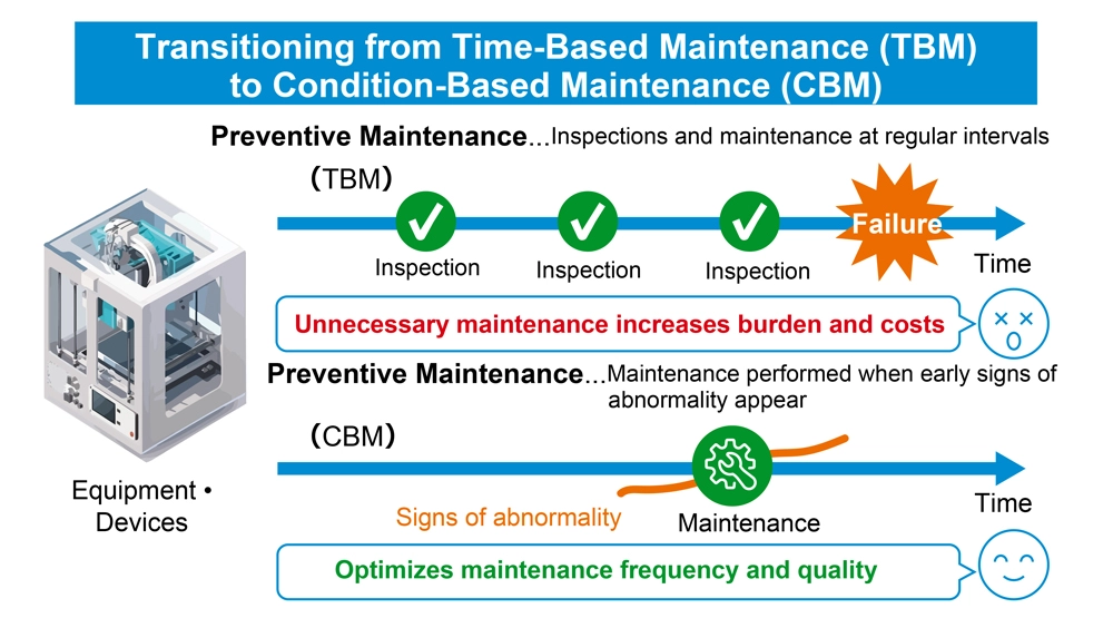
In the manufacturing industry, equipment maintenance has traditionally relied on preventive maintenance (TBM: Time-Based Maintenance), where inspections and part replacements are carried out at predetermined intervals. While effective to a degree, this approach often requires shutting down equipment that is still operating normally, resulting in unnecessary downtime, higher operating costs, and increased workload on production sites. In some cases, excessive inspection tasks can even introduce the problems they are intended to prevent—such as mistakes and human error.
Consequently, many manufacturers are now transitioning to predictive maintenance (CBM: Condition-Based Maintenance), which monitors equipment conditions in real time and performs maintenance only when early signs of abnormality are detected.
This white paper examines Solist-AI, ROHM’s AI-driven solution that enhances the efficiency and reliability of predictive maintenance.
- Transitioning from Time-Based Maintenance (TBM) to Condition-Based Maintenance (CBM)
The primary difference between preventive maintenance (TBM) and predictive maintenance (CBM) lies in how maintenance timing is determined. TBM schedules inspections and part replacements at fixed time intervals, independent of the equipment’s actual condition. In contrast, CBM performs maintenance only when truly necessary. AI plays a critical role in CBM by continuously monitoring parameters such as temperature, vibration, and current through sensors, processing large volumes of time-series data, and detecting early signs of abnormality from subtle pattern deviations.
By adopting predictive maintenance, manufacturers can avoid unnecessary shutdowns of equipment that is still operating normally. AI-driven optimisation of maintenance timing reduces operational costs and workload, while also preventing excessive inspections that may introduce procedural or human errors. Furthermore, because CBM ensures consistent maintenance quality without relying on technician intuition or experience, it is gaining attention as an effective solution to on-site challenges such as the shortage of skilled workers and persistent labour shortages.
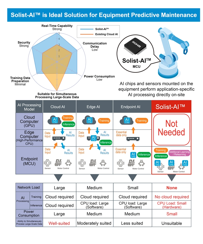
- Shifting from Cloud-Based to Endpoint-Based Architecture
Conventional cloud-based AI systems face several challenges, including communication latency, the complexity of building and maintaining network infrastructure, and the added burden of implementing security measures to prevent data leaks during transmission.
These systems also require large volumes of training data to be collected and prepared in advance, making it difficult to account for variations in operating environments and equipment-specific differences at each site. High-precision AI processing also demands significant computational resources such as CPUs and GPUs, which inevitably increases power consumption.
This has led to the growing adoption of endpoint AI as a more practical alternative. By performing both learning and inference directly on devices equipped with sensors and MCUs, endpoint AI can adapt to the characteristics of individual machines, perform real-time processing, and maintain exceptionally low power consumption. In addition, because no data is transmitted to the cloud, it ensures a high level of security.
To support this paradigm, ROHM developed Solist-AI, an on-device AI solution optimised for edge computing, which is the core technology behind predictive maintenance. The name is derived from ‘Solution with On-device Learning IC for Standalone AI.’ Just like a ‘solist’ in music who performs independently, Solist-AI completes the entire AI workflow, from learning to inference, locally on the device without relying on the cloud or external networks.
While Solist-AI delivers significant advantages for on-device AI, it is not designed for large-scale data processing or image-based workloads compared to conventional AI architectures (cloud, edge, or endpoint types). For advanced analytics, such as detailed image diagnostics, cloud-based AI remains the preferred solution.
For applications that do not require advanced analysis, Solist-AI offers a major benefit: substantial cost savings by eliminating expenses associated with network infrastructure and cloud service fees.
And with ongoing learning capabilities, Solist-AI can continuously update its understanding of equipment deterioration over time. This greatly improves responsiveness to both normal and abnormal conditions as machines age, making it a compelling alternative to traditional AI solutions.
- Solist-AI: The Optimal Solution for Predictive Maintenance
Unlike general-purpose AI processors, Solist-AI is purpose-built for targeted use cases such as failure prediction and anomaly detection. The ability to train and fine-tune models directly on-site based on the actual operating environment ensures flexible adaptation to equipment variations and changing ambient conditions.
At the heart of the solution is the Solist-AI MCU, which integrates ROHM’s proprietary AI accelerator AxlCORE-ODL (On-Device Learning). This accelerator performs a three-layer neural network and FFT (Fast Fourier Transform) processing in dedicated hardware, enabling real-time detection and notification of various anomalies and operational changes in the field.

The biggest advantage of Solist-AI lies in its simplicity as a standalone AI system, requiring only a sensor and MCU. Whereas conventional AI solutions depend on cloud access or network connectivity, Solist-AI operates completely independent of any network infrastructure. This allows it to be easily retrofitted into existing equipment while eliminating concerns related to communication delays and data leakage.
Equipped with a built-in AI accelerator, AxlCORE-ODL learns and infers data from sensors–such as vibration, temperature, and current—— in real time. By quantifying subtle deviations from normal patterns, it identifies and alerts users to early signs of abnormality.
Operating at an exceptionally low power level of approximately 40 mW, Solist-AI stands in stark contrast to conventional cloud-based AI systems that typically consume anywhere from 2W to 200W. This makes it well-suited for battery-powered devices and ideal for retrofitting into existing equipment. As a result, it enhances maintenance and operational efficiency across a wide range of industrial assets, including robots, motors, and cooling fans.
In addition, a variety of support tools are available, including Solist-AI Sim, which enables preliminary verification of AI suitability, and Solist-AI Scope, which offers real-time visualisation of AI behaviour. These tools enable implementation and evaluation without requiring specialised AI expertise, greatly lowering the barrier to adoption.

Example of Integration with AE (Acoustic Emission) Sensors
Combining AE sensors and Solist-AI enables high precision detection of abnormalities that are extremely difficult to identify manually, such as insufficient bearing lubrication or microscopic surface damage. The system analyses multiple AE sensor outputs (including peak amplitude, average value, energy, and event count) across multiple dimensions. The AI numerically quantifies the degree of abnormality, allowing early detection of emerging issues and supporting timely, condition-based maintenance. Because the progression of anomaly levels can be visually understood without requiring specialised expertise, this solution is widely regarded for its suitability in real-world on-site operation.
- Summary
ROHM’s Solist-AI is a true endpoint solution that functions independently of the cloud, delivering a practical approach to predictive maintenance. By completing both learning and inference in real-time using only a sensor and MCU, it eliminates the need for network connectivity, consumes very low power, and offers robust security for safe, reliable operation. Dedicated support tools allow even personnel without AI expertise to easily deploy and evaluate the system.
A wide range of proven application examples, including detecting abnormal fan motor vibrations and identifying changes in current waveforms, demonstrate how Solist-AI substantially lowers the barriers to implementation.
Going forward, ROHM is expanding the product lineup and developing higher-performance models to support broader use across maintenance and other applications. Solist-AI brings new value to manufacturing sites by quickly detecting ‘deviations from normal’ on the factory floor and autonomously prompting appropriate actions
To help engineers learn more about and fully leverage Solist-AI, ROHM invites users to connect through a dedicated community, ‘Solist-AI Open Lab: Getting Started’ on its technical platform, Engineer Social Hub (available in Japanese; registration/login required). In addition to accessing detailed information on Solist-AI, members can ask questions, share feedback, and discuss evaluation and implementation challenges, so we encourage you to participate.
The post Shifting from preventive maintenance to predictive maintenance appeared first on ELE Times.
How Can the High Voltage Intelligent Battery Shunt Reference Design Benefit You?
Courtesy: Element 14
Introduction
Accurate current measurement is a critical aspect of modern electrical engineering. Precision is essential everywhere – from battery management systems (BMS) to industrial automation. Traditional sensing methods are inadequate when temperatures fluctuate, leading to unreliable readings.
That’s where shunt resistors come to the rescue. These components produce a small, measurable voltage drop that reflects the amount of current flowing through them. However, their performance can be influenced by changes in temperature, which alter resistance and distort measurements. The temperature coefficient of resistance (TCR) quantifies this change, making low TCR shunt resistors essential for high precision applications.
Vishay’s WSBE8518 shunt resistor exemplifies such precision. Vishay offers the HV-IBSS-USB reference design – a sophisticated tool that simplifies testing and integration – to streamline its evaluation. This article explores the function of shunt resistors, the significance of low TCR, the impact of thermal drift, and how the HV-IBSS-USB reference design empowers engineers to achieve accurate current sensing in demanding environments.
Understanding Shunt Resistors in Current Sensing
A shunt resistor, also known as a current shunt resistor or an ammeter shunt, is a low resistance component placed in series with a load to measure voltage drop when current flows through it. This voltage drop, measured by an analogue-to-digital converter (ADC), is directly proportional to the current, enabling accurate current measurement using Ohm’s Law.
Shunt resistors are vital in precision current sensing across a wide range of high-reliability applications. These include monitoring charge and discharge cycles in BMS for electric vehicles (EV), energy storage systems, and portable devices, regulating output and detecting overcurrent in power supplies and motor control systems. Renewable energy setups like solar inverters and wind turbines ensure accurate power flow measurement, while industrial automation provides critical feedback for diagnostics and system reliability. They are also indispensable in network UPS systems, power meters, and high-precision environments such as aerospace and defence applications, where even minor deviations in current measurement can have critical consequences.
Selecting a shunt resistor involves balancing its resistance value, power rating, and TCR. For instance, the WSBE8518, with a 100 μΩ resistance and 36 W power rating at 70 °C, produces a 50 mV drop at 500 A – making it suitable for high current applications while maintaining accuracy. The WSBE series can support up to 1825 A with no noticeable resistance shift.
 Figure 1: A comparison of current measurement stability over temperature between Vishay’s Intelligent Battery Shunt System (IBSS) and a competing shunt
Figure 1 demonstrates that as the temperature rises from 25 °C to 80 °C, the standard shunt (in red) shows a current reading drift from 200 A to over 200.6 A, while Vishay’s (in blue) remains nearly flat at 200 A, highlighting its superior thermal stability. Vishay also delivers cleaner, less noisy measurements, unlike the standard shunt’s non-linear, noisier signal response.
Why Does TCR Matter in Precision Sensing?
Resistance isn’t constant—it changes with temperature. The TCR quantifies this change, expressed in parts per million per degree Celsius (ppm/°C). In simple terms, TCR tells us how much a resistor’s value will drift as the temperature fluctuates.
If a resistor has a positive TCR, its resistance increases with rising temperature. A negative TCR means resistance decreases as it gets warmer. In either case, too much variation can compromise measurement accuracy. A low TCR is critical in precision current sensing, especially in systems where even the slightest error can cascade into larger problems. Due to increased electron scattering, most metals naturally see resistance rise with temperature. However, specialized alloys — such as the manganese-copper used in Vishay’s WSBE8518 shunt resistor —can achieve remarkably stable performance, with TCRs as low as ± 10 ppm/°C. This makes them ideal for applications demanding high accuracy under wide temperature swings.
For instance, a 1 mΩ shunt with a TCR of ± 50 ppm/°C will experience a resistance change of ± 5 µΩ over a 100 °C temperature swing, which is equivalent to ± 0.5 % of its nominal resistance. That may seem insignificant, but in high precision environments such as battery charge balancing or power regulation, such deviations can skew current readings and disrupt system performance. The following equation calculates the maximum change in resistance value for a given TCR:
R = R0 X 1 [ 1 + α(T-T0)]
where,
R = final resistance
R0 = initial resistance
α = TCR
T = final temperature
T0 = initial temperature
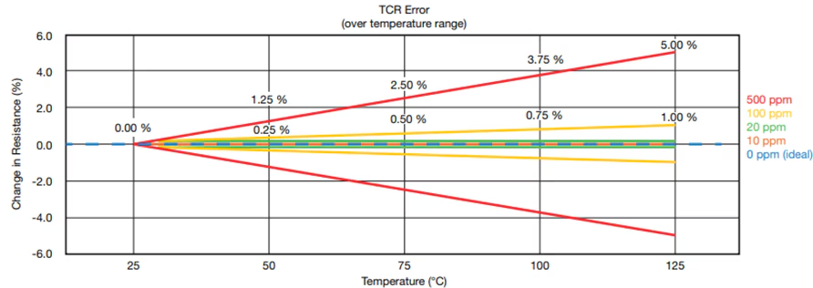 Figure 2: This graph compares different TCR levels as a percentage change in resistance versus increasing temperature from 25 °C
The benefits of low TCR are:
- Improved measurement accuracy: With resistance remaining stable across temperature variations, current sensing becomes more precise
- Better thermal stability: Minimal resistance drift, even under fluctuating ambient conditions or due to self-heating from applied power
- Ideal for high precision circuits: Supports applications that require consistent performance over wide temperature ranges
- Enhanced performance in harsh environments: Suitable for military and high-temperature electronics where reliability under thermal stress is critical
- Minimizes error in Kelvin configurations: Particularly advantageous in 4-terminal setups in which precise voltage sensing is critical
Figure 3 illustrates the superior thermal stability of WSBE series resistors (NiCr and CuMn) compared to standard shunt resistors. While the standard shunt exhibits a large resistance drift over temperature (indicative of poor TCR), the WSBE resistors maintain almost constant resistance across a broad thermal range.
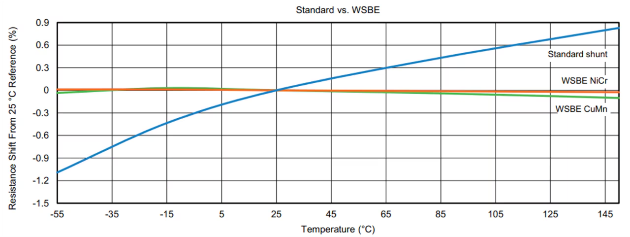 Figure 3: TCR comparison chart (WBSE series vs a standard shunt resistor)
Understanding Thermal Drift in Current Sensing
Thermal drift refers to changes in a component’s electrical characteristics caused by fluctuations in temperature. In shunt resistors, thermal drift alters resistance, directly affecting current measurement accuracy. For instance, copper, with a TCR of 3900 ppm/°C, can exhibit a 39 % resistance change over a 100 °C temperature range, severely compromising precision. Low TCR materials, such as the manganese-copper alloy in the WSBE8518, reduce this effect, maintaining high measurement accuracy.
Thermal drift can also arise from self-heating due to power dissipation during operation. Vishay’s HV-IBSS-USB mitigates this by combining a low TCR shunt with an efficient circuit design, minimizing temperature-induced errors. Kelvin (4-terminal) connections further enhance accuracy by reducing the impact of high TCR copper terminals, enabling consistent and repeatable measurements.
How the Reference Design Works
The HV-IBSS-USB reference design features two isolated domains: an HV analog front-end and an LV digital control section. Powered and interfaced via USB, the LV side hosts a microcontroller that manages data acquisition and communication. Power is transferred to the HV domain through a charge pump, where precision 22-bit sigma-delta ADCs and carefully selected analog components enable high-resolution current and voltage measurements.
The design compensates for thermal drift through automatic gain and offset calibration, ensuring accuracy across temperature variations. A dedicated voltage divider feeds the voltage signal directly to the ADC, eliminating amplifier drift. An NTC-based converter transmits a PWM signal across the isolation barrier for temperature monitoring. Data is available via a virtual COM port, auto-detected over USB, enabling seamless integration with PC-based tools.
- Current measurement: a third-order delta-sigma modulator converts the voltage drop across the WSBE8518 shunt into a digital signal, with automatic gain and offset calibration. The shunt’s TCR (10 ppm/°C) outperforms the analog circuitry’s drift (33.6 ppm/°C), ensuring high accuracy
- Voltage measurement: a 22-bit sigma-delta ADC measures voltage, divided by the CDMA2512 resistor to fit the ADC’s range
Temperature measurement: an NTC thermistor and multivibrator convert temperature to a frequency signal, transmitted as a PWM signal to the microcontroller
 Figure 5: Functional block diagram of the HV-IBSS-USB
Application: EVs
In BMS for EVs and other compact mobility vehicles such as electric two-wheelers, precise current measurement is critical for monitoring charge and discharge cycles, balancing cells, and ensure safe, efficient operation. The HV-IBSS-USB facilitates the evaluation of the WSBE8518 shunt in these demanding environments. Installed in series with the high voltage battery pack, the shunt accurately measures currents up to 500 A, which is ideal for applications where currents routinely exceed 100 A.
The reference design’s USB-C interface enables real-time data logging, allowing engineers to analyze current flow, detect anomalies, and fine-tune battery management algorithms. The WSBE8518’s low TCR ensures accurate measurements even as operating temperatures rise during rapid charging or high load discharge. Voltage measurements spanning 10 V to 850 V and integrated temperature sensing provide additional data for detecting faults or optimizing power distribution.
A typical application circuit places the shunt between the EV battery and the drive or charging system. The HV-IBSS-USB’s HV+ and HV + terminals connect to the shunt’s Kelvin terminals, and the USB-C port links to a computer for data acquisition and analysis.
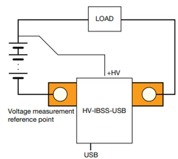 Figure 6: Typical application circuit
Conclusion
As current sensing requirements continue to tighten across EVs, energy storage, and high-power industrial systems, accuracy can no longer be left vulnerable to temperature effects and component drift. Vishay’s HV-IBSS-USB reference design, built around the ultra-low-TCR WSBE8518 shunt resistor, addresses this challenge head-on by combining material stability, Kelvin sensing, high-resolution ADCs, and intelligent calibration in a ready-to-evaluate platform. By minimizing thermal drift and simplifying high-voltage, high-current measurements, the design enables engineers to validate performance quickly, reduce development risk, and deploy more reliable battery and power management systems. In applications where every milliamp matters, the HV-IBSS-USB offers a practical pathway from precision measurement theory to real-world, production-ready accuracy.
The post How Can the High Voltage Intelligent Battery Shunt Reference Design Benefit You? appeared first on ELE Times.
The Move to 48 Volts in Transportation
Courtesy: Avnet
| Key Takeaways:
● 48V systems are being adopted in mobility, industrial, data centres, and automotive ● Higher voltage brings multiple benefits ● New 48V motor control kit offers flexibility and efficiency ● Battery management included |
Shifting to 48V isn’t just about higher voltage. What stands out here is how that shift enables lighter designs, longer battery life, and more efficient operation. Think drones that fly further, autonomous robots that run longer without a recharge, and electric vehicles that pack more punch without bulking up.
For OEMs looking at a new product line or planning upgrades, that’s more than a technical specification; it’s a competitive factor. Getting ahead of this voltage transition could mean catching the next wave in smart transportation and industrial automation.
The market’s responding, not just in automotive, but across sectors like logistics, warehousing, and even consumer robotics.
Put 48V on your roadmap
For teams evaluating roadmap priorities, the takeaway is that aligning with this voltage shift isn’t optional. It’s quickly becoming a baseline expectation for future-ready platforms.
NXP has introduced a high-power 48V motor control kit, and there’s quite a bit under the hood here. You’ve got flexibility for controlling single three-phase, dual three-phase, and single six-phase setups, plus compatibility with resolver, hall, and encoder sensors. That means it’s well-positioned for teams with complex motor demands. Those motors could be driving a range of applications, from drones to autonomous or guided robots.
From a strategic standpoint, having isolated communication and redundant power supply isn’t just a feature; it’s risk mitigation. Fault protection for things like overcurrent and overheating? That’s a game-changer for operational uptime. Add functional safety to the mix. It’s built for both industrial and automotive standards, so teams don’t have to choose between performance and compliance.
Development kit availability
Launch timing is crucial. NXP’s development kit is available from December for early access, but the full rollout lands in January. Contact your Avnet representative to register your interest. NXP is also bundling standard drivers and control libraries, so the barrier to entry is lower for engineering teams.
For OEMs that need deeper customisation, there’s a premium software tier with extra safety features and source code. The architecture is modular, too: controller board, adapter board, power stage, and heat sink, with motors left out for flexibility. That setup is deliberate, letting customers tailor the kit to their own requirements, rather than locking them into a one-size-fits-all hardware solution.
 The NXP development kit will be generally available from January 2026, with early access available by contacting your Avnet representative.
NXP MCUs are at the core, plus a GUI for streamlined control. It’s aimed at making deployment straightforward, whether for prototyping or scaling up production. That level of integration should make it easier for teams to hit aggressive timelines while still meeting compliance and quality bars.
Battery management for 48V systems
Let’s shift the focus to battery management. If you’re investing in next-gen mobility or industrial systems, BMS is at the heart of every decision. What’s new here is the scale. The product family now covers everything from 12 volts all the way up to 1500 volts, but the 48V range is the sweet spot for cost and flexibility. That’s not just for cars; it’s a fit for industrial energy storage, drones, and autonomous robots.
That creates a broader footprint, but what’s the real differentiator between these 48V solutions and the legacy setups? First, you’re seeing devices like the BMA 7518 that are exclusive to 48V, with others bridging up to higher voltages in industrial use. Certification’s a key lever. Everything’s aiming for ISO 26262 on the automotive side and IEC 61508 for industrial. Compliance isn’t just a checkbox; it moves the needle on market access and risk.
There’s a new software stack for active cell balancing, and “battery passport” tools are being rolled out to keep up with European compliance. Secure protocols are another layer, making sure the system’s ready for upcoming requirements. NXP is not just filling out the product line; it’s building for future-proofing and regulatory headwinds.
Early access to 48V solutions
Avnet is working with NXP to provide early access for select customers. If you’re aiming to build momentum before January, this is a real lever for market entry. By prioritising hands-on pilots and direct feedback loops, teams catch issues or feature requests early in the cycle.
If you are evaluating 48V systems, contact your Avnet representative to find out how you could benefit from these exciting developments.
The post The Move to 48 Volts in Transportation appeared first on ELE Times.
Сторінки

