
Новини світу мікро- та наноелектроніки
My Smart Wall Clock
 | I designed the case myself. Use esp32-c3 with WifiManager library. The time updates automatically:) [link] [comments] |
Just started the ICL7135-based multimeter
 | Yes, I will try to build a precise voltage/current measurment equipment from scratch just for fun. Wish me luck. One step at a time: - 5-digit multiplexed display with the К176ИД2 driver - MC34063 negative rail DC-DC converter - 555 timer 120kHz click source - REF3333 precise voltage reference [link] [comments] |
University of Sheffield to lead £12.5m UK Centre for Heterogeneous Integrated MicroElectronic and Semiconductor Systems
Low-cost MCUs enable smarter embedded devices

Leveraging ST’s 40-nm process and an Arm Cortex-M33 core, STM32C5 MCUs deliver increased speed for cost-sensitive embedded devices. The microcontrollers run faster than many entry-level chips, improving the capabilities of compact smart devices in factories, homes, cities, and infrastructure while keeping dynamic power consumption low (<80 µA/MHz).

Running at 144 MHz and achieving a CoreMark score of 593, the Cortex-M33 offers up to three times the performance of typical Cortex-M0+ devices. ST’s 40-nm cost-efficient manufacturing process supports higher clock speeds and larger on-chip memory. The STM32C5 series integrates 128 KB to 1024 KB of flash and 64 KB to 256 KB of RAM.
The MCUs are designed to meet SESIP3 and PSA Level 3 security requirements, with memory protection, tamper protection, cryptographic engines, and temporal isolation to protect processes such as secure boot and firmware updates. Variants with additional security provide hardware unique key support, secure key storage, and hardware cryptographic accelerators for symmetric and asymmetric operations.
The STM32C5 MCUs are entering production now and are available in packages ranging from 20 to 144 pins. Pricing starts at $0.64 each in 10,000-unit quantities.
The post Low-cost MCUs enable smarter embedded devices appeared first on EDN.
TinyEngine NPU powers AI in TI MCUs

TI’s MSPM0G5187 and AM13E23019 MCUs integrate the TinyEngine NPU, enabling efficient edge AI in systems ranging from simple to complex. These latest additions to TI’s portfolio of AI-enabled hardware, software, and tools allow engineers to deploy intelligence anywhere. This announcement moves TI closer to its goal of integrating the TinyEngine NPU across its entire microcontroller lineup.

The MSPM0G5187 is powered by an Arm Cortex-M0+ 32-bit core operating at up to 80 MHz and includes 128 KB of flash. Its TinyEngine NPU is capable of running AI models with up to 90× lower latency and more than 120× less energy per inference than comparable MCUs without an accelerator. By performing neural-network computation locally, the NPU operates in parallel with the primary CPU running application code. Priced at under $1 in 1,000-unit quantities, the MSPM0G5187 brings edge AI to simpler, smaller, and lower-cost applications.
Aimed at real-time motor control, the AM13E23019 leverages an Arm Cortex-M33 32-bit core operating at up to 200 MHz and includes 512 KB of flash. It maintains precise real-time control loops for up to four motors while the TinyEngine NPU runs adaptive control algorithms. An integrated trigonometric math accelerator performs calculations 10× faster than coordinate rotation digital computer (CORDIC) implementations, enabling more responsive motor control.
The MSPM0G5187 is available now in production quantities on TI.com, while the AM13E23019 is currently available in preproduction quantities.
The post TinyEngine NPU powers AI in TI MCUs appeared first on EDN.
Edge AI SoC integrates tri-radio

The i.MX 93W applications processor from NXP combines a dedicated AI NPU with secure tri-radio wireless connectivity in a single package. By eliminating the need for up to 60 discrete components, the SoC reduces board area, design complexity, and system-level costs.

Purpose-built to accelerate physical AI deployment, the i.MX 93W is supported by NXP’s software stack, eIQ AI enablement tools, and precertified reference designs that simplify RF integration. The device integrates a dual-core Arm Cortex-A55 processor and an Arm Ethos NPU capable of up to 1.8 eTOPS. Wireless connectivity is provided by the IW610 tri-radio, supporting Wi-Fi 6, Bluetooth Low Energy, and IEEE 802.15.4 for Matter and Thread.
The i.MX 93W SoC integrates an EdgeLock Secure Enclave (Advanced Profile) to support device security and regulatory frameworks such as the European Cyber Resilience Act. The enclave provides a hardware root of trust for secure boot, updates, device attestation, and device access. With NXP’s EdgeLock 2GO key management service, devices can be provisioned during manufacturing or in the field.
The i.MX 93W is slated to begin sampling in the second half of 2026.
The post Edge AI SoC integrates tri-radio appeared first on EDN.
200-V MOSFETs cut conduction losses

Two devices have joined iDEAL Semiconductor’s SuperQ 200-V MOSFET portfolio, offering very low RDS(on) in standard power packages. These two SuperQ devices are designed for demanding motor-drive applications that require high efficiency, robustness, and fault tolerance.

The iS20M5R5S1T achieves a maximum RDS(on) of just 5.5 mΩ in the compact TOLL package, enabling higher power density and reduced conduction losses in space-constrained designs. Similarly, the iS20M6R3S1P delivers a maximum RDS(on) of 6.3 mΩ in the rugged TO-220 package, providing high efficiency for applications that favor through-hole assembly, mechanical mounting, or direct heatsinking.
The new SuperQ MOSFETs feature high short-circuit withstand current and closely matched gate thresholds, with a variation of ±0.5 V, for easier paralleling. They are rated for 175 °C and can handle currents up to 151 A in the TOLL package and 172 A in the TO-220 package. Both devices are avalanche-rated and undergo 100% UIS testing in production.
In addition to motor drives, these MOSFETs are also suitable for switched-mode power supplies, secondary-side synchronous rectification, and other high-current industrial or battery-powered systems.
The iS20M5R5S1T and iS20M6R3S1P are in volume production and available through iDEAL’s global distribution channels.
The post 200-V MOSFETs cut conduction losses appeared first on EDN.
Sfera Labs debuts industrial Raspberry Pi edge systems

Sfera Labs has introduced an industrial Raspberry Pi-based edge server and PLC for industrial IoT and edge applications. The Strato Pi Plus server and Iono Pi v3 controller come in DIN-rail enclosures with an embedded Raspberry Pi 4 or 5 single-board computer (SBC), delivering industrial-grade systems for automation, field communications, and IoT edge deployments that require continuous, unattended operation.

The Strato Pi Plus features a hybrid architecture that pairs the Raspberry Pi SBC with an RP2354 MCU. The RP2354 operates independently of the main processor to manage critical real-time functions and system supervision, including an independent hardware watchdog. In-field firmware updates for the RP2354 are supported via OTA, managed directly through the Raspberry Pi. Serial connectivity includes four individually opto-isolated RS-485 ports and one CAN FD interface. The Strato Pi Plus operates from an integrated 10–50 V DC supply with surge and reverse-polarity protection and a 3.3 A resettable fuse.
The Iono Pi v3 industrial PLC integrates a 9–28 V DC power supply, four power relays, high-resolution analog voltage and current inputs, and seven configurable GPIO pins. Like the Strato Pi Plus, it implements a hardware watchdog in the RP2354 MCU that operates independently of the Raspberry Pi SBC. The device also includes a real-time clock with a temperature-compensated oscillator and replaceable backup battery. An embedded Microchip ATECC608 secure element enables hardware-based authentication and cryptographic key storage.
A timeline for availability of the Strato Pi Plus and Iono Pi v3 was not provided at the time of this announcement.
The post Sfera Labs debuts industrial Raspberry Pi edge systems appeared first on EDN.
I built a text-to-schematic CLI tool
 | There are a lot of "AI generates hardware" claims floating around, and most of them produce garbage. I've been working on a tool called boardsmith that I think does something actually useful, and I want to show what it really outputs rather than making abstract claims. Here's what happens when you run boardsmith build -p "ESP32 with BME280 temperature sensor, SSD1306 OLED, and DRV8833 motor driver" --no-llm: You get a KiCad 8 schematic with actual nets wired between component pins. The I2C bus has computed pull-up resistors (value based on bus capacitance with all connected devices factored in). Each IC has decoupling caps with values per the datasheet recommendations. The power section has a voltage regulator sized for the total current budget. I2C addresses are assigned to avoid conflicts. The schematic passes KiCad's ERC clean. You also get a BOM with JLCPCB part numbers (191 LCSC mappings), Gerber files ready for fab upload, and firmware that compiles for the target MCU. The ERCAgent automatically repairs ERC violations after generation. boardsmith modify lets you patch existing schematics ("add battery management") without rebuilding. And boardsmith verify runs 6 semantic verification tools against the design intent (connectivity, bootability, power, components, BOM, PCB). The tool has a --no-llm mode that's fully deterministic — no AI, no API key, no network. The synthesis pipeline has 9 stages and 11 constraint checks. It's computing the design, not asking a language model to guess at it. Where it falls short: 212 components in the knowledge base (covers common embedded parts, but you'll hit limits). No high-speed digital design — no impedance matching, no differential pairs. No analog circuits — no op-amp topologies, no filter design. Auto-placed PCB layout is a starting point, not a finished board. It's fundamentally a tool for the "boring" part of embedded design — the standard sensor-to-MCU wiring that experienced engineers can do in their sleep but still takes 30 minutes. Open source (AGPL-3.0), built by a small team at ForestHub.ai. I'd love feedback from people who actually design circuits — is this solving a real annoyance, or am I in a bubble? [link] [comments] |
CEA-Leti and NcodiN partner to industrialize 300mm silicon photonics for bandwidth-hungry AI interconnects
CCTV Controller - Running on a RP2040 Microcontroller using circuit python KMK firmware for switching between camera feeds
 | I posted this a bit ago for the keyboard diode matrix I made. Please ignore the shoddy soldering on the prototype board lol. But this project has been my first dive into microcontrollers, and after watching some videos on how easy circuit python KMK firmware ( https://github.com/KMKfw/kmk\_firmware ) was to install and configure I just knew I had to do it. In essence this thing is just a clunky big macro board that I made as a proof of concept before I make a nicer one. The software it's intended to be used with is a bit of python that I used gemini / chatgpt to make ( https://github.com/IvoryToothpaste/rtsp-viewer ) that maps all the camera feeds to a specific hotkey via the config file. This thing was a lot of fun to make, and I'm excited to post the final version of everything :) [link] [comments] |
ROHM’s TRCDRIVE pack, HSDIP20 and DOT-247 silicon carbide molded power modules now available online
Impact of AI on Computing and the Criticality of Testing
Courtesy: Teradyne
Artificial intelligence (AI) is transforming industries, enhancing our daily lives, and improving efficiency and decision-making, but its need for computing power is growing at an astonishing rate, doubling every three months (Figure 1). To maintain this pace, the semiconductor industry is moving beyond traditional chip development – it has entered the era of heterogeneous chiplets in advanced integrated packages.
 (Figure 1: The Growth of Compute Requirements. Source: https://openai.com/index/ai-and-compute/)
The Rise of Chiplets
Chip companies like NVIDIA and AMD are rewriting the rules, designing architectures that combine multiple CPUs and GPUs in a single advanced package along with high bandwidth memory (HBM). AI workloads require rapid access to vast amounts of data, made possible by integrating HBMs. This approach, combining two, four, or more processing cores with HBM stacks, requires a complex, advanced packaging technique developed by TSMC called CoWos® – Chip-on-Wafer-on-Substrate, typically referred to as 2.5/3D packaging (Figure 2). These packages can exceed 100 mm x 100 mm in size and will require wafer interposer probers that can handle large CoW modules/stacks and also meet significantly larger thermal dissipation requirements, as discussed below.
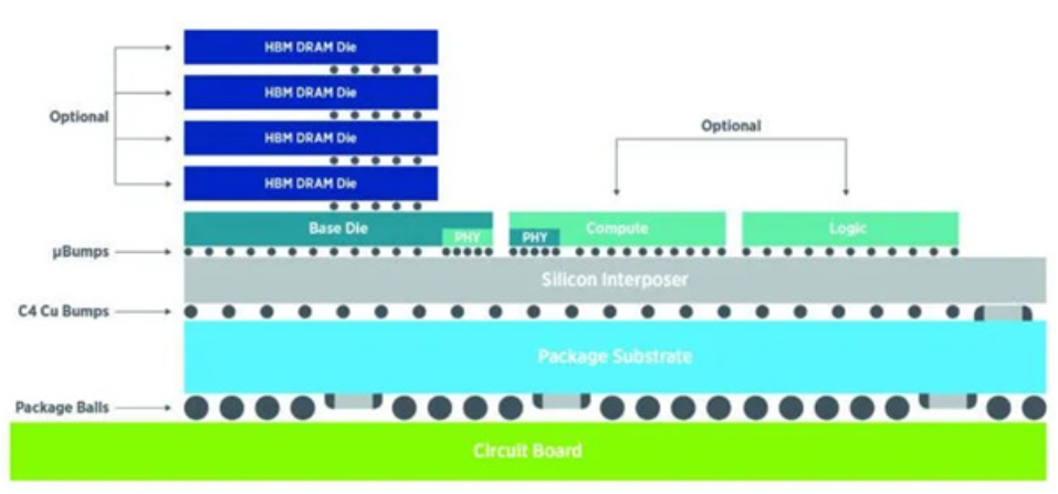 (Figure 2: 2.5D/3D packaging architecture, Source: Teradyne)
To maintain peak performance, these heterogeneously integrated advanced packaging devices need proprietary high-speed interfaces to communicate efficiently. All these requirements contribute to an increasingly complex semiconductor landscape.
Testing Becomes More Complex in Step with Chip Advancements
As package complexity increases, so does the need for more deliberate test strategies. In the transition from monolithic dies to chiplets, long-established test methods are not always directly transferable because test IP is now distributed across multiple dies and, in some cases, across different design teams or companies. This fragmentation requires a clearer definition of what must be tested at each stage—die, bridge, interposer, substrate, and stack—and which standards or techniques apply to each scope.
Packing multiple dies into a single chiplet-based system is a major advancement, but it raises a key challenge: verifying that every component functions correctly before final assembly. Multi-die packages require rigorous screening to avoid yield loss, and it is not enough to qualify only the dies. Interposers, substrates, bridges, and stacks also need to be validated, using test techniques appropriate to each layer. The industry is thus moving into “known-good-everything”, from known-good-die (KGD) to known-good-interposer (KGI), to known-good-CoW (KG-CoW), and so on. (Figure 3)
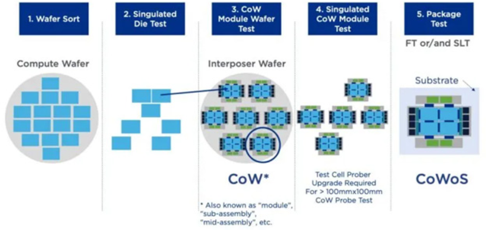 (Figure 3: Possible test insertions to ensure KGD and KG-CoW. Source: Teradyne)
High-speed communication between chiplets introduces an additional layer of complexity. Dies must exchange data at extreme speeds – such as during GPU-to-HBM transfers – yet their physical and electrical interfaces vary by manufacturer. Open standards like Universal Chiplet Interconnect Express (UCIe ) continue to evolve, but chiplet interfaces still differ widely. To support this diversity, test solutions increasingly need interface IP that behaves like the device’s native protocol to avoid electrical overstress or probe-related damage. Some suppliers now offer UCIe-compliant PHY and controller IP that device makers can integrate, enabling automated test equipment (ATE) platforms to test high-speed links safely and consistently.
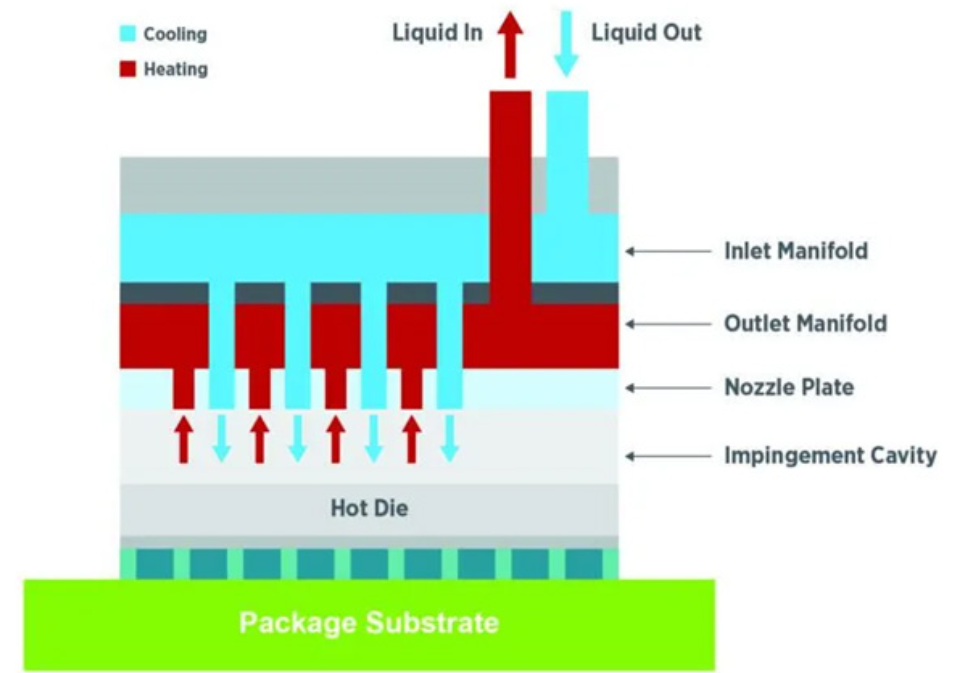 (Figure 4: Chip-level bare cooling, Source: Teradyne)
Manufacturers and test operators must also pay close attention to thermal management. More processing power means more heat dissipation issues, requiring advanced cooling methods – perhaps even liquid cooling inside the package itself (Figure 4). More die in the package means more connections, and thus, more resources are needed in the tester. More transistors mean higher power supply current requirements, more power supply instruments, and an increased set of thermal challenges that demand innovative cooling solutions and advanced adaptive thermal control (ATC) strategies.
Lastly, manufacturing test operations must consider the interposer, a physical interface layer that electrically connects a chip to a substrate or other active component. For example, a multilayer or 2.5D package includes multiple dies on an interposer assembled on top of a substrate. That interposer functions as a mini silicon board, routing signals from the upper floor die to the bottom floor die. It’s critical that the interposer is also a known good die or known good interposer (KGI) to ensure adequate yields for advanced packages.
The Future of AI and Semiconductor Testing
There has been an uptick in industry recognition that semiconductor testing is an integral part of today’s chiplet and advanced packaging trend. As this unfolds, AI computing will continue its pace of unprecedented evolution, relying on semiconductor testing to fill a crucial role in ensuring quality devices get to market in the shortened timelines today’s market demands. Semiconductor test will remain the unsung hero of AI-driven computing, steadily enabling the next wave of technological breakthroughs.
The post Impact of AI on Computing and the Criticality of Testing appeared first on ELE Times.
A long-ago blow leads to water overflow: Who could know?

Mechanical analogies to electronics symbols are common in other engineering disciplines. We might refer to this one, then, as akin to a battery with an internal short circuit?
I’ll warn you upfront that this particular blog post has nothing specific to do with electronics (aside, I suppose, from the potential for electrocution caused by a water-soaked calamity). That said, I’ll also postulate upfront that (IMHO, at least) it has a great deal to do with engineering in general, specifically as it exemplifies the edge and corner cases that were the subject of a 2.5+ year back previous post from yours truly. Read on or not, as you wish. That said, I hope you’ll proceed!
I kicked off that prior writeup with the following prose:
Whether or not (and if so, how) to account for rarely encountered implementation variables and combinations in hardware and/or software development projects is a key (albeit often minimized, if not completely overlooked) “bread and butter” aspect of the engineering skill set… I’ve always found case studies about such anomalies and errors fascinating, no matter that I’ve also found them maddening when I’m personally immersed in them!
Speaking of the personal angle…and immersion, for that matter…
At our peak, my wife and I have had (several times so far…blame me, not her) up to five four-legged mammal companions concurrently sharing our residence with us. Therein explaining the sizeable (4-gallon/15-liter reservoir) Petmate Aspen Pet Lebistro Cat and Dog Water Dispenser that we bought through Amazon at the beginning of 2020:

Amazon’s packaging robustness can be hit-and-miss; when this particular order arrived at our front door, the reservoir and base were detached and loose. And the outer box contained no packing material, far from inner boxes for either/both constituent piece(s). Unsurprisingly, therefore, the reservoir tank had a dent in one corner (the below is a more recent picture…keep reading):

I pushed it back into place as best I could:

and then filled-and-tested the tank, which still seemed to be watertight. And then, driven by a broader longstanding abhorrence for sending functionally sound albeit cosmetically compromised stuff to the landfill, I decided to keep it and press it into service, accompanied by a successful partial-refund request made to Amazon customer service.
Fast-forward six years. We’re down (for the moment, at least) to only one (canine) companion, a factoid which as you’ll soon see likely ended up being key. And we started finding puddles of standing water in proximity to the water dispenser on the (watertight vinyl, thankfully) laundry room floor. Did we initially accuse the dog of bumping into the dispenser, causing spills? Yes, we did. Did subsequent observation convince us that our initial theory was off base? Yes, it did. And did we then feel badly for unjustly initially blaming the dog? Yes…we did. Bad humans. Bad!
In-depth painstaking engineering analysis (cough) eventually led to the realization that the water spills were preceded by slow-but-sure filling of the bowl all the way to the lip (and then beyond, therefore the puddles), versus the inch-below-the-lip level that the dispenser traditionally stuck to. But what had changed? Figuring this out required that I first learn about how gravity water bowls function in the first place. How do they initially fill only to the inch-below-the-lip level, and how do they then automatically maintain this level as the water is consumed by canine and feline companions, until drained (if one of the humans had forgotten to refill it, that is)?
I learned the answer from, as I’m more generally finding of late, Reddit. Specifically, from a post in the cleverly named “Explain Like I’m Five” subreddit (I’m doing my best not to take offense) titled “How do self-filling/gravity fed pet water bowls not overflow and spill everywhere?”. The entire discussion thread is fascinating, again IMHO, containing exchanges such as the following:
- ender42y: This works for a stack up to 32 ft or 9 meters tall (at standard atmospheric pressure) at which point the top of the water tank would actually start to form a vacuum.
- bloc97: It is a bit shorter in practice as the water will start to boil at ~2 kpa (assuming 20c).
- MindStalker: That’s exactly why you are limited to a column that’s about 9 meters tall, anything above that boils away.
- bloc97: Yes, as there are two processes that determines the column height (density and vapor pressure of the fluid), we just need to make sure not to confuse the two.
Again: . That said, have I yet admitted what a devoted follower of the TV personality Mr. Wizard I was as a wee lad (we didn’t have YouTube back then)?
That admission explains (more than) a few things, yes? Speaking of vacuums, here’s the “money quote” from that Reddit post thread, with kudos to Redditor nestcto:
Recapping the basics, the opening acts as both the exit for the water, and the entrance for air. The air is obviously needed because under normal circumstances, you can’t just have nothing in the bottle. The water must be replaced with something. That’s where the air comes in.
So making the water leave the bottle is easy. You just have to make sure the water is creating more outward pressure to leave the bottle, than the vacuum inside trying to replace it with air.
To keep the water in, you have to make sure the water can’t create more pressure to leave the bottle than the vacuum trying to suck in air. This is more difficult because water is heavy, so gravity pushes it down a lot. The more water, the more pressure. The more pressure, the easier to overcome the vacuum.
Viscosity is a factor here as well, that I won’t go into too much. Basically, the thicker something is, the harder it is to get through a small opening.
Water isn’t very thick, but it’s much thicker than air. So there’s a point where the opening is small enough that water has trouble getting through it without some pressure behind it. The force of gravity isn’t strong enough to push the water through the small opening, and the internal vacuum is too weak to suck air in since no water has left yet to create a vacuum. So there’s a standstill.
When this happens, you may notice that you can actually make the water flow outwards by agitating the bottle. Take a needle or toothpick, and swish it around the opening. You’ll notice that some water leaves the bottle. This causes a small vacuum to replace the water. Which sucks in air. The air displacing the water to rise upwards can destabilize gravitational pressure towards the opening, causing more water to leave, and more air to come in, and next thing you know, the whole thing is emptying due to a cycle of pressure. Water out. Vacuum created. Air in. Vacuum satisfied. Water out. Vacuum created…and so on.
Now, the point at which you reach that standstill depends on a LOT of factors. But it’s pretty much always a lot easier to accomplish with less water, because you have less downward pressure to fight against due to gravity.
Ok, that’s all well and good. But it still doesn’t explain why my “self-filling/gravity fed pet water bowl” “destabilized”, as nestcto referred to it. For that, keep scrolling through the thread (admittedly, I particularly resonated, for different reasons, with the last two):
- MrBulletPoints: Yeah if you were to jam something sharp into the top of that setup and make a hole, it would allow air in and the bowl would definitely overflow
- verronbc: Yeah… I like to call myself smart sometimes. The first bowl like this we had our dumb 70 lb dog was scared of the bubbles it made after he drank a bit out of the bowl. My simple solution, “Oh, I know I’ll just drill a hole in the top then the air will fill from the top” yeah in a moment of weakness I forgot exactly why and how these work and caused a lot of water to drain on the floor. My girlfriend still teases me about it.
- [deleted]: That’s why you have to punch a hole in the beer can before you shotgun it. It’s the same concept.
- stoic_amoeba: As an engineer, I’ve genuinely had this idea cross my mind because the bowl is HEAVY when you fill it all the way. Also, as engineer, I’m a bit ashamed I didn’t immediately realize how bad an idea that’d be. I haven’t done it, thank goodness, but I should know better.
Ahem. At least some of you likely realize what happened next. I went back and looked at that reservoir again, eventually realizing that after six years, the dent had finally become slightly compromised. If I filled the reservoir, turned upside-down from its normal position (so it was resting on its top), left it in the sink and waited a long time, I’d eventually find that a few drops of water had leaked out of it.
The same compromise was true (in reverse) for air, of course, when it was oriented correctly and in place. And it very well might have been like this for a while, counterbalanced by the frequent water intake of multiple pets. Drop the count down to one dog, though, and…puddles. We replaced it with a smaller dispenser from the same manufacturer, the first example of which also arrived from Amazon dented, believe it or not (I shipped it back for replacement this time):

and we’re happily back to an always-dry floor again.
I’ll close with a few photos of the original base, both initially intact and then disassembled:


The way these things work is that, after filling the reservoir with water, you screw on the lid:

then turn it upside down and quickly rotate it to lock it in place here:

The lid’s hole diameter is also key, by the way, as I learned one time when I put the reservoir in place without remembering to screw on the lid first (speaking of water all over the floor)…
Note the gap around the repository where the lid fits. I’m guessing this is where the air comes from to replace the displaced water in the reservoir, but I haven’t come across another Reddit thread to supplement my ignorance on this nuance. Reader insights on this, or anything else which my case study has stimulated, are as-always welcome in the comments!
—Brian Dipert is the Principal at Sierra Media and a former technical editor at EDN Magazine, where he still regularly contributes as a freelancer.
Related Content
The post A long-ago blow leads to water overflow: Who could know? appeared first on EDN.
Advanced Aerospace Materials: Driving Hypersonic, Stealth and High-Efficiency Defence Systems
By- Shreya Bansal, Sub-Editor
The aerospace and defence sector is undergoing a materials revolution driven by escalating performance demands that conventional alloys and composites can no longer meet. As military and commercial aircraft push toward hypersonic speeds, extended operational ranges, and stealth capabilities, traditional materials face fundamental limitations in thermal tolerance, weight-to-strength ratios, and electromagnetic properties. This article examines the current landscape of advanced materials, including ceramic matrix composites, high-entropy alloys, graphene-enhanced structures, and metamaterials that are displacing legacy materials in critical applications.
The transition isn’t merely about incremental improvement; it represents a paradigm shift in how aerospace components are designed and manufactured. Engineers are abandoning materials that have dominated the industry for decades in favour of solutions that enable previously impossible capabilities: jet engines operating at temperatures that would melt nickel super alloys, airframe structures that self-repair micro-damage, and radar-absorbing surfaces engineered at the molecular level. Through expert interviews with materials scientists and aerospace engineers, this article explores why this transition is happening now, what technical and economic factors are driving adoption, and which materials are positioned to define the next generation of aerospace and defence systems.
The Materials Revolution Redefining Aerospace and DefenceThe aerospace and defence sector is undergoing a profound materials transformation. As aircraft and defence systems push toward hypersonic velocities, extended mission endurance, lower radar signatures, and improved fuel efficiency, conventional materials such as aluminium alloys, titanium, and nickel-based superalloys are reaching their performance ceilings.
The next generation of aerospace capability is no longer driven solely by aerodynamics or propulsion; it is increasingly defined by materials science. From ceramic matrix composites (CMCs) that withstand temperatures exceeding traditional alloy limits to high-entropy alloys (HEAs) engineered at the atomic scale, advanced materials are enabling systems once considered technologically unattainable.
Vern Benson, Northrop Grumman Technical Fellow (2026):
“Previous generations of aircraft were mostly made of metal, while newer versions are approximately 50% composite materials, with an even higher percentage for military aircraft… In order to compete with metals, we have to be highly automated in our manufacturing process.”
For decades, aerospace engineering relied on aluminium alloys, titanium, and nickel-based superalloys as the backbone of structural and propulsion systems. These materials delivered an optimal balance of strength, weight, corrosion resistance, and manufacturability for subsonic and supersonic flight regimes. However, modern mission profiles, ranging from hypersonic vehicles and advanced fighter aircraft to long-endurance unmanned systems, have exposed the inherent limitations of these conventional materials. Aluminium alloys lose strength rapidly at elevated temperatures, titanium becomes cost-prohibitive at scale, and nickel superalloys are approaching their thermal operating thresholds in next-generation turbine engines. As propulsion systems push for higher combustion temperatures to improve efficiency, and as airframes demand lighter structures to extend range and payload capacity, traditional materials no longer provide sufficient performance margins. These realities have shifted material selection from being a secondary design consideration to a primary performance enabler in aerospace and defence programs. Conventional materials, while proven and reliable, were engineered for a different era of performance requirements. Aluminium alloys struggle under extreme thermal loads. Titanium offers strength but at a weight and cost penalty. Nickel superalloys approach thermal limits in advanced jet engines.
Baba Kalyani, Chairman & MD, Bharat Forge (2025):
“At a time of heightened geopolitical and supply-chain uncertainty… the emphasis is firmly on upgrading platforms, systems and technologies… we must emerge as an ‘Innovation driven Economy’ that manufactures and exports best-in-class products.”
Hypersonic systems and next-generation combat aircraft demand materials that can endure sustained extreme heat while maintaining structural integrity. The tipping point for abandoning traditional materials often occurs during thermal modelling or fatigue simulations, where safety margins erode under mission stress scenarios.
Engineers are increasingly identifying material limitations during early-stage digital twin simulations, triggering a search for advanced alternatives before physical prototyping even begins.
Ceramic Matrix Composites and High-Entropy Alloys: From Research to RealityAdvanced materials such as ceramic matrix composites (CMCs) and high-entropy alloys (HEAs) are redefining what aerospace components can endure. CMCs, for example, can withstand temperatures hundreds of degrees higher than conventional superalloys while weighing significantly less. Their integration into turbine shrouds and combustor liners has enabled engines developed by companies such as GE Aerospace to operate at higher efficiencies while reducing cooling requirements. Similarly, HEAs, engineered with multiple principal elements rather than one dominant base metal, exhibit exceptional strength, oxidation resistance, and thermal stability. These materials are transitioning from laboratory experimentation to production-grade deployment, driven by advances in additive manufacturing and precision powder metallurgy. What was once considered experimental is now becoming operational, marking a fundamental shift in aerospace material qualification and deployment timelines.
Five years ago, advanced materials comprised a niche percentage of aerospace structural systems. Today, in next-generation engines and airframes, they are becoming integral rather than experimental.
Lifecycle Economics: Justifying Advanced Material InvestmentWhile advanced materials often command higher upfront costs, their value becomes evident when evaluated over the full lifecycle of an aerospace platform. Lighter airframes reduce fuel consumption, directly lowering operational expenditures and emissions. Higher-temperature engine materials increase thermodynamic efficiency and reduce maintenance frequency. Extended component durability minimises downtime and replacement cycles, factors critical for both commercial airlines and military operators. Leaders at organisations such as RTX Corporation have emphasised that procurement decisions are increasingly based on total ownership cost rather than acquisition price alone. Moreover, as production volumes scale and supply chains mature, the cost gap between conventional and advanced materials continues to narrow. When assessed across decades of operational service, advanced materials frequently offer compelling economic advantages despite their initial premium.
Fuel savings, extended maintenance intervals, and enhanced durability can offset initial procurement premiums.
Yet supply chain maturity remains a gating factor. Dependency on rare earth elements, specialised ceramic fibres, or advanced powder metallurgy inputs introduces geopolitical and availability risks.
Government R&D partnerships, particularly in the U.S., Europe, and Asia, have played a critical role in de-risking early-stage adoption by subsidising demonstration programs and pilot manufacturing lines.
Manufacturing Evolution: Scaling Advanced Materials SafelyThe adoption of advanced materials requires a parallel transformation in manufacturing methodologies and quality assurance frameworks. Unlike traditional metal alloys that rely on well-established forging and casting processes, materials such as CMCs and ultra-high-temperature ceramics demand specialised fabrication techniques, including fibre weaving, matrix infiltration, and controlled sintering. Additive manufacturing has further expanded possibilities, enabling complex geometries that were previously impossible to machine. However, these innovations introduce new challenges in inspection, certification, and scalability. Companies like Boeing are investing heavily in digital twins, advanced non-destructive evaluation methods, and automated production systems to ensure reliability and repeatability. Successfully integrating advanced materials into flight-ready systems requires not only material innovation but also synchronised advances in manufacturing science, workforce training, and regulatory certification standards.
Dr. G. Satheesh Reddy, Former Chairman, DRDO (2025):
“While precision manufacturing of the stealth airframe is critical, the speciality materials, including RAM (Radar Absorbent Material), have already been developed… Manufacturing the aircraft itself won’t be a challenge if we work entirely from the provided designs and material lists with disciplined scaling.”
CMC production, for instance, requires precision fibre weaving and matrix infiltration processes not used in conventional metallurgy. Quality assurance shifts from visual inspection and ultrasonic testing to advanced microstructural evaluation.
Organisations must also retrain engineers and technicians in new fabrication techniques, creating workforce transition challenges alongside technological ones.
Strategic and Geopolitical Implications of Materials LeadershipIn aerospace and defence, materials innovation is no longer purely a technical matter; it is a strategic asset. Advanced composites enable stealth characteristics through radar absorption and electromagnetic manipulation. Ultra-high-temperature ceramics support hypersonic weapon systems capable of withstanding extreme aerodynamic heating. Lightweight structures extend operational reach and payload flexibility, enhancing mission effectiveness. As global competition intensifies, control over critical materials, precursor chemicals, and advanced manufacturing capabilities has become a national security priority. Organisations such as Airbus and major U.S. defence contractors increasingly view materials science as a pillar of competitive differentiation. Nations investing heavily in advanced material research are positioning themselves to define the performance boundaries of next-generation aircraft, spacecraft, and defence platforms.
From a defence perspective, material science leadership is increasingly viewed as a domain of geopolitical competition similar to semiconductors and AI. Control over precursor materials, advanced manufacturing capabilities, and a proprietary composite formulation carries strategic weight.
Dependence on foreign-sourced rare materials or advanced fibres presents vulnerabilities that governments are actively addressing through domestic production incentives.
Looking Ahead – The Next Frontier in Aerospace MaterialsLooking ahead, the next frontier in aerospace materials will be shaped by computational design, artificial intelligence, and sustainability imperatives. AI-driven materials discovery platforms can simulate atomic interactions and predict performance characteristics before physical prototypes are fabricated, dramatically accelerating development cycles. At the same time, environmental considerations are becoming central to material selection. Recyclable composites, bio-derived resins, and low-emission manufacturing processes are gaining traction as aerospace companies commit to long-term decarbonization goals. Future “smart materials” may combine self-healing properties, adaptive electromagnetic behaviour, and extreme thermal resistance within a single multifunctional structure. As aerospace systems grow more complex and mission demands intensify, the integration of digital engineering and advanced materials science will define the trajectory of innovation for decades to come. AI-driven materials discovery platforms now simulate atomic structures and predict performance before physical synthesis, dramatically reducing time-to-certification.
Future “dream materials” would combine:
- Extreme thermal resistance
- Structural strength
- Lightweight properties
- Electromagnetic tunability
- Sustainability
Such materials would enable sustained hypersonic travel, near-zero-emission propulsion systems, and adaptive stealth platforms.
The post Advanced Aerospace Materials: Driving Hypersonic, Stealth and High-Efficiency Defence Systems appeared first on ELE Times.
Disruptions from Wide Bandgap Continue Turbulence
Courtesy: Avnet
When we experience major shifts in the technology landscape, we should expect disruption and turbulence. OEMs, suppliers and distributors are coming together to navigate rough waters.
The shift from conventional silicon toward wide bandgap (WBG) substrates for power applications, predominantly Silicon Carbide (SiC) and Gallium Nitride (GaN), isn’t without its challenges. The supply chain for WBG solutions is now maturing, which means we’re seeing consolidation, acquisition and even some attrition.
This turbulence, while a cause for concern, is predictable and surmountable. Confidence in WBG technology remains high, but the market conditions and geopolitical risks must be acknowledged as contributing factors.
New applications are exhibiting polarised conditions. Demand for electric vehicles (EVs) has plateaued in some regions, while the thirst for AI data centres seems unquenchable. Both are served by WBG devices. The technological benefits of WBG are clear, but challenges around its use can still be a barrier. Recently, we asked SiC market leader onsemi for its thoughts and recommendations.
With a fully vertically integrated supply chain, from crystal growth to final packaging, onsemi is addressing scalability, quality control and cost efficiencies in-house. While it sees yield and the transition from 150mm to 200mm wafers as ongoing challenges, demand volatility can cause inventory fluctuations. This is a key contributor to the turbulence we’re seeing, but it’s part of the natural evolution of new technology.
Partnerships with companies including Vitesco and Magna, and long-term agreements are part of onsemi’s strategy to secure supply and fund capacity expansion. Its recent acquisition of Qorvo’s SiC JFET technology and the United Silicon Carbide subsidiary further strengthened its position.
The impact of increased demand
As demand increases, higher volumes will drive down per-unit pricing, which justifies the investments being made in larger wafer sizes and new fabs. Onsemi currently operates fabs and packaging facilities in multiple regions, helping to avoid supply chain disruptions related to geopolitical tensions and export controls.
As capacity expands due to demand, suppliers will see higher returns on their investments. This will support the industry’s virtuous cycle of investment in capacity. As technology matures, production volumes and yields improve and lead to greater process stability. Also, onsemi contributes to JEDEC (Joint Electron Device Engineering Council), Automotive Electronics Council (AEC) and the European Centre for Power Electronics’ Working Group “Automotive Qualification Guidelines” (AQG) to define SiC standards, which promote stability and interoperability between suppliers.
Turbulence will give way to stability
WBG is a transformative technology. It brings benefits to critical applications, including EVs, AI data centers and renewable energy. The strategic investments being made by suppliers, such as onsemi, demonstrate the industry’s commitment.
Pairing the right technology with key applications is crucial. For example, data centre power and circuit protection are applications where SiC JFETs are differentiated by their low on-resistance and switching frequencies, surpassing GaN and even SiC MOSFETs.
Market conditions and the challenges of adopting new technology are contributing to the turbulence we’re seeing in the market. But demand continues to grow, paving the way to stability.
The post Disruptions from Wide Bandgap Continue Turbulence appeared first on ELE Times.
Scintil releases DWDM laser source evaluation kit for scale-up AI networks
GaN fundamentals: 2DEG, crystal structure, and figure of merit

Gallium nitride (GaN) power devices are redefining the limits of switching converters by combining wide bandgap physics with lateral HEMT structures optimized for fast, low-loss operation. This article describes GaN as the natural successor to silicon MOSFETs in the 100–650 V class, showing how material figures of merit directly translate into lower on-resistance, higher switching frequency, and much higher power density at competitive cost.
Silicon power MOSFETs have driven the evolution of switch-mode power conversion since the late 1970s, replacing bipolar transistors, thanks to majority-carrier operation, ruggedness, and ease of drive. For decades, continuous structural improvements—cell pitch, trench, and superjunction—pushed RDS(on) down while keeping breakdown capability and manufacturability. However, silicon is now essentially at its theoretical limit for unipolar devices in the 100–600 V range.
The bandgap of a semiconductor is related to the strength of the chemical bonds between the atoms in the lattice. Stronger bonds make it more difficult for electrons to transition between atomic sites. This leads to several important consequences, including lower intrinsic leakage currents and the ability to operate at higher temperatures. Based on scientific data, both GaN and silicon carbide (SiC) exhibit significantly wider bandgaps than silicon.
The theoretical specific on-resistance RDS(on) of a majority-carrier device is constrained by the material’s critical electric field, permittivity, and mobility. For a one square millimeter device area, the drift region controls the trade-off between breakdown voltage and conduction loss.
The approximate breakdown voltage can be written as:
VBR = ½ wdrift Ecrit
wdrift is the drift region thickness and Ecrit is the material’s critical electric field.
The number of electrons available in the drift region between two terminals is calibrated by a simplified, one-dimensional Poisson relation:
q ND = ε0 εr Ecrit wdrift
Where q is the electron charge, ND the doping concentration (or equivalent electron density), ε0 the vacuum permittivity, and εr the relative permittivity.
Combining this with the usual expression for resistance of the drift region (for area = 1 mm²) results in the below equation:
RDS(on) = w_drift / (q μn ND)
It yields the well-known relation between specific on-resistance and breakdown voltage:
RDS(on) = 4 VBR² / (ε0 εr μn Ecrit³)
This equation shows the dominant role of the critical field: RDS(on) scales as VBR² but inversely as Ecrit³. A material that can withstand a much higher electric field and maintain good mobility will deliver orders of magnitude lower specific resistance at the same breakdown voltage.

Figure 1 See theoretical on-resistance for a one square millimeter device versus blocking voltage capability for Si-, SiC-, and GaN-based power devices. Source: Efficient Power Conversion (EPC)
In Figure 1, silicon, 4H-SiC, and GaN theoretical limits diverge dramatically as breakdown voltage increases. At 600 V, GaN’s theoretical specific RDS(on) is roughly two orders of magnitude lower than silicon, and significantly better than SiC, highlighting why GaN is particularly attractive in the 100–650 V class.
Crystal structure and 2DEG formation
GaN’s crystal structure is a key enabler for these performance gains. Crystalline GaN adopts a wurtzite hexagonal structure, while 4H-SiC also has a hexagonal lattice but with different stacking. Both materials are mechanically robust, chemically stable, and tolerant of high operating temperatures, but GaN additionally exhibits strong piezoelectric effects due to the asymmetry of the wurtzite lattice. This effect brings GaN to achieve very high conductivity compared with either silicon or silicon carbide.
When a thin layer of AlGaN is grown on top of GaN, lattice mismatch and spontaneous polarization create strain at the interface. This strain, combined with the intrinsic polarization of the wurtzite structure, generates a strong internal electric field. To compensate this, a two-dimensional electron gas (2DEG) forms at the AlGaN/GaN interface with sheet carrier density on the order of 1013 cm-2 and electron mobility significantly higher than bulk GaN (up to 1500–2000 cm²/V·s versus ~1000 cm²/V·s). This ultra-thin, highly conductive channel is at the heart of the GaN HEMT.

Figure 2 Simplified cross section of a GaN/AlGaN heterostructure shows the formation of a 2DEG created due to the strain-induced polarization at the interface between the two materials. Source: Efficient Power Conversion (EPC)
From an electrical standpoint, this 2DEG behaves like a very low-resistance sheet: the product of carrier density and mobility (ns μn) is much higher than in a doped silicon drift region, while the conduction path is extremely short and lateral. This combination is what allows GaN devices to reach very low RDS(on) for a given chip area and breakdown rating. In addition, the wide bandgap (3.39 eV vs. 1.12 eV for silicon) yields much lower intrinsic leakage and supports higher operating temperatures.
GaN, SiC, and silicon: Material figures of merit
Let’s compare key material parameters for Si, GaN, and 4H-SiC: bandgap, critical field, electron mobility, permittivity, and thermal conductivity. Both SiC and GaN have wider bandgap and much higher critical fields than silicon. In addition to its wide bandgap, GaN exhibits significantly higher electron mobility than both silicon and silicon carbide, enabling faster carrier transport, higher current density, and superior high-frequency performance.
Moreover, GaN’s Ecrit is about 3.3 MV/cm, compared to 0.23 MV/cm for silicon, allowing a much thinner drift region for the same breakdown voltage. The previous RDS(on)–VBR equation directly shows that increasing Ecrit reduces the specific on-resistance by orders of magnitude.
Silicon carbide has even better thermal conductivity than GaN, which is an advantage for very high-power densities and high-voltage systems (>1 kV). However, in the mid-voltage range up to a few hundred volts, GaN’s combination of lateral HEMT structure, very high Ecrit, and 2DEG conduction gives it a superior theoretical figure of merit compared to both silicon and SiC. This positions GaN as the primary technology for replacing MOSFETs in most 40–650 V applications.
From depletion-mode to enhancement-mode GaN HEMTs
The native GaN HEMT is a depletion-mode device: at zero gate bias the 2DEG under the AlGaN barrier provides a low-resistance channel between source and drain, and a negative gate voltage is required to pinch it off. Source and drain contacts reach the 2DEG through the AlGaN layer, while the gate sits on top and modulates the channel by depleting or restoring that electron gas.
This normally-on behavior is acceptable in RF power amplifiers, but it’s problematic in switching converters, where a device that conducts at VGS = 0 V can cause shoot-through during startup or fault conditions.
For power conversion, enhancement-mode operation (normally-off) is therefore essential. With an enhancement-mode HEMT, the 2DEG is suppressed at zero gate bias and re-formed only when a positive gate voltage is applied, making its behavior similar to a power MOSFET.
Several device architectures implement this transition from depletion- to enhancement-mode:
- In recessed-gate structures, the AlGaN barrier is locally thinned beneath the gate. Reducing the barrier thickness lowers the internal polarization-induced field to the point where the 2DEG vanishes at VGS = 0 V. A positive gate voltage then recreates the channel and allows current to flow.
- Fluorine-implanted gates introduce negative charge into the AlGaN barrier by ion implantation. The fixed negative charge depletes the 2DEG under the gate at zero bias, shifting the threshold into the positive range. Applying a positive gate voltage compensates this charge and restores conduction.
- In p‑GaN gate HEMTs, a thin p-type GaN layer is grown on top of the AlGaN barrier. The positive charge in this p-GaN region creates a built‑in potential that overcomes the polarization field and depletes the 2DEG at zero gate bias. When a positive voltage is applied to the gate, electrons are again attracted to the interface and the 2DEG reforms, turning the device on.
- Hybrid solutions combine a low-voltage enhancement-mode silicon MOSFET with a depletion-mode GaN HEMT in series. In the cascode configuration, the MOSFET gate becomes the external control terminal. When the MOSFET turns on, the GaN gate is effectively driven to a voltage that enables the HEMT; when the MOSFET turns off, the GaN gate is driven negative, and the composite behaves as a normally‑off device.
All these approaches pursue the same goal: eliminate conduction at VGS = 0 V using an architecture that remains compatible with practical gate‑drive levels and offers stable threshold voltage. In practice, p‑GaN gate devices have become the most widely used in commercial power conversion, while cascode hybrids are attractive at higher voltages where the on‑resistance of the silicon MOSFET adds only a small penalty to the GaN device.

Figure 3 An enhancement-mode (e-mode) device depletes the 2DEG with zero volts on the gate (a). By applying a positive voltage to the gate, the electrons are attracted to the surface, re-establishing the 2DEG (b). Source: Efficient Power Conversion (EPC)
The second and final part of this article series about GaN technology fundamentals will explain hybrid structures and RDS(on) penalty as well as vertical GaNs and how to build a GaN HEMT transistor.
 Maurizio Di Paolo Emilio is director of global marketing communications at Efficient Power Conversion (EPC), where he manages worldwide initiatives to showcase the company’s GaN innovations. He is a prolific technical author of books on GaN, SiC, energy harvesting and data acquisition and control systems, and has extensive experience as editor of technical publications for power electronics, wide bandgap semiconductors, and embedded systems.
Editor’s Note:
The content in this article uses references and technical data from the book GaN Power Devices for Efficient Power Conversion (Fourth Edition) authored by Alex Lidow, Michael de Rooij, John Glaser, Alejandro Pozo Arribas, Shengke Zhang, Marco Palma, David Reusch, Johan Strydom.
Related Content
- SiC vs. GaN: Who wins
- The advantages of Vertical GaN Technology
- A brief history of gallium nitride (GaN) semiconductors
- A new IDM era kickstarts in the gallium nitride (GaN) world
- New GaN Technology Makes Driving GaN-Based HEMTs Easier
The post GaN fundamentals: 2DEG, crystal structure, and figure of merit appeared first on EDN.
Navitas appoints former Lattice chief accounting officer as CFO
Navitas adds top-side-cooled QDPAK and low-profile TO-247-4L to package line-up in 5th-generation GeneSiC technology
Сторінки

