
Новини світу мікро- та наноелектроніки
Scintil releases DWDM laser source evaluation kit for scale-up AI networks
GaN fundamentals: 2DEG, crystal structure, and figure of merit

Gallium nitride (GaN) power devices are redefining the limits of switching converters by combining wide bandgap physics with lateral HEMT structures optimized for fast, low-loss operation. This article describes GaN as the natural successor to silicon MOSFETs in the 100–650 V class, showing how material figures of merit directly translate into lower on-resistance, higher switching frequency, and much higher power density at competitive cost.
Silicon power MOSFETs have driven the evolution of switch-mode power conversion since the late 1970s, replacing bipolar transistors, thanks to majority-carrier operation, ruggedness, and ease of drive. For decades, continuous structural improvements—cell pitch, trench, and superjunction—pushed RDS(on) down while keeping breakdown capability and manufacturability. However, silicon is now essentially at its theoretical limit for unipolar devices in the 100–600 V range.
The bandgap of a semiconductor is related to the strength of the chemical bonds between the atoms in the lattice. Stronger bonds make it more difficult for electrons to transition between atomic sites. This leads to several important consequences, including lower intrinsic leakage currents and the ability to operate at higher temperatures. Based on scientific data, both GaN and silicon carbide (SiC) exhibit significantly wider bandgaps than silicon.
The theoretical specific on-resistance RDS(on) of a majority-carrier device is constrained by the material’s critical electric field, permittivity, and mobility. For a one square millimeter device area, the drift region controls the trade-off between breakdown voltage and conduction loss.
The approximate breakdown voltage can be written as:
VBR = ½ wdrift Ecrit
wdrift is the drift region thickness and Ecrit is the material’s critical electric field.
The number of electrons available in the drift region between two terminals is calibrated by a simplified, one-dimensional Poisson relation:
q ND = ε0 εr Ecrit wdrift
Where q is the electron charge, ND the doping concentration (or equivalent electron density), ε0 the vacuum permittivity, and εr the relative permittivity.
Combining this with the usual expression for resistance of the drift region (for area = 1 mm²) results in the below equation:
RDS(on) = w_drift / (q μn ND)
It yields the well-known relation between specific on-resistance and breakdown voltage:
RDS(on) = 4 VBR² / (ε0 εr μn Ecrit³)
This equation shows the dominant role of the critical field: RDS(on) scales as VBR² but inversely as Ecrit³. A material that can withstand a much higher electric field and maintain good mobility will deliver orders of magnitude lower specific resistance at the same breakdown voltage.

Figure 1 See theoretical on-resistance for a one square millimeter device versus blocking voltage capability for Si-, SiC-, and GaN-based power devices. Source: Efficient Power Conversion (EPC)
In Figure 1, silicon, 4H-SiC, and GaN theoretical limits diverge dramatically as breakdown voltage increases. At 600 V, GaN’s theoretical specific RDS(on) is roughly two orders of magnitude lower than silicon, and significantly better than SiC, highlighting why GaN is particularly attractive in the 100–650 V class.
Crystal structure and 2DEG formation
GaN’s crystal structure is a key enabler for these performance gains. Crystalline GaN adopts a wurtzite hexagonal structure, while 4H-SiC also has a hexagonal lattice but with different stacking. Both materials are mechanically robust, chemically stable, and tolerant of high operating temperatures, but GaN additionally exhibits strong piezoelectric effects due to the asymmetry of the wurtzite lattice. This effect brings GaN to achieve very high conductivity compared with either silicon or silicon carbide.
When a thin layer of AlGaN is grown on top of GaN, lattice mismatch and spontaneous polarization create strain at the interface. This strain, combined with the intrinsic polarization of the wurtzite structure, generates a strong internal electric field. To compensate this, a two-dimensional electron gas (2DEG) forms at the AlGaN/GaN interface with sheet carrier density on the order of 1013 cm-2 and electron mobility significantly higher than bulk GaN (up to 1500–2000 cm²/V·s versus ~1000 cm²/V·s). This ultra-thin, highly conductive channel is at the heart of the GaN HEMT.

Figure 2 Simplified cross section of a GaN/AlGaN heterostructure shows the formation of a 2DEG created due to the strain-induced polarization at the interface between the two materials. Source: Efficient Power Conversion (EPC)
From an electrical standpoint, this 2DEG behaves like a very low-resistance sheet: the product of carrier density and mobility (ns μn) is much higher than in a doped silicon drift region, while the conduction path is extremely short and lateral. This combination is what allows GaN devices to reach very low RDS(on) for a given chip area and breakdown rating. In addition, the wide bandgap (3.39 eV vs. 1.12 eV for silicon) yields much lower intrinsic leakage and supports higher operating temperatures.
GaN, SiC, and silicon: Material figures of merit
Let’s compare key material parameters for Si, GaN, and 4H-SiC: bandgap, critical field, electron mobility, permittivity, and thermal conductivity. Both SiC and GaN have wider bandgap and much higher critical fields than silicon. In addition to its wide bandgap, GaN exhibits significantly higher electron mobility than both silicon and silicon carbide, enabling faster carrier transport, higher current density, and superior high-frequency performance.
Moreover, GaN’s Ecrit is about 3.3 MV/cm, compared to 0.23 MV/cm for silicon, allowing a much thinner drift region for the same breakdown voltage. The previous RDS(on)–VBR equation directly shows that increasing Ecrit reduces the specific on-resistance by orders of magnitude.
Silicon carbide has even better thermal conductivity than GaN, which is an advantage for very high-power densities and high-voltage systems (>1 kV). However, in the mid-voltage range up to a few hundred volts, GaN’s combination of lateral HEMT structure, very high Ecrit, and 2DEG conduction gives it a superior theoretical figure of merit compared to both silicon and SiC. This positions GaN as the primary technology for replacing MOSFETs in most 40–650 V applications.
From depletion-mode to enhancement-mode GaN HEMTs
The native GaN HEMT is a depletion-mode device: at zero gate bias the 2DEG under the AlGaN barrier provides a low-resistance channel between source and drain, and a negative gate voltage is required to pinch it off. Source and drain contacts reach the 2DEG through the AlGaN layer, while the gate sits on top and modulates the channel by depleting or restoring that electron gas.
This normally-on behavior is acceptable in RF power amplifiers, but it’s problematic in switching converters, where a device that conducts at VGS = 0 V can cause shoot-through during startup or fault conditions.
For power conversion, enhancement-mode operation (normally-off) is therefore essential. With an enhancement-mode HEMT, the 2DEG is suppressed at zero gate bias and re-formed only when a positive gate voltage is applied, making its behavior similar to a power MOSFET.
Several device architectures implement this transition from depletion- to enhancement-mode:
- In recessed-gate structures, the AlGaN barrier is locally thinned beneath the gate. Reducing the barrier thickness lowers the internal polarization-induced field to the point where the 2DEG vanishes at VGS = 0 V. A positive gate voltage then recreates the channel and allows current to flow.
- Fluorine-implanted gates introduce negative charge into the AlGaN barrier by ion implantation. The fixed negative charge depletes the 2DEG under the gate at zero bias, shifting the threshold into the positive range. Applying a positive gate voltage compensates this charge and restores conduction.
- In p‑GaN gate HEMTs, a thin p-type GaN layer is grown on top of the AlGaN barrier. The positive charge in this p-GaN region creates a built‑in potential that overcomes the polarization field and depletes the 2DEG at zero gate bias. When a positive voltage is applied to the gate, electrons are again attracted to the interface and the 2DEG reforms, turning the device on.
- Hybrid solutions combine a low-voltage enhancement-mode silicon MOSFET with a depletion-mode GaN HEMT in series. In the cascode configuration, the MOSFET gate becomes the external control terminal. When the MOSFET turns on, the GaN gate is effectively driven to a voltage that enables the HEMT; when the MOSFET turns off, the GaN gate is driven negative, and the composite behaves as a normally‑off device.
All these approaches pursue the same goal: eliminate conduction at VGS = 0 V using an architecture that remains compatible with practical gate‑drive levels and offers stable threshold voltage. In practice, p‑GaN gate devices have become the most widely used in commercial power conversion, while cascode hybrids are attractive at higher voltages where the on‑resistance of the silicon MOSFET adds only a small penalty to the GaN device.

Figure 3 An enhancement-mode (e-mode) device depletes the 2DEG with zero volts on the gate (a). By applying a positive voltage to the gate, the electrons are attracted to the surface, re-establishing the 2DEG (b). Source: Efficient Power Conversion (EPC)
The second and final part of this article series about GaN technology fundamentals will explain hybrid structures and RDS(on) penalty as well as vertical GaNs and how to build a GaN HEMT transistor.
 Maurizio Di Paolo Emilio is director of global marketing communications at Efficient Power Conversion (EPC), where he manages worldwide initiatives to showcase the company’s GaN innovations. He is a prolific technical author of books on GaN, SiC, energy harvesting and data acquisition and control systems, and has extensive experience as editor of technical publications for power electronics, wide bandgap semiconductors, and embedded systems.
Editor’s Note:
The content in this article uses references and technical data from the book GaN Power Devices for Efficient Power Conversion (Fourth Edition) authored by Alex Lidow, Michael de Rooij, John Glaser, Alejandro Pozo Arribas, Shengke Zhang, Marco Palma, David Reusch, Johan Strydom.
Related Content
- SiC vs. GaN: Who wins
- The advantages of Vertical GaN Technology
- A brief history of gallium nitride (GaN) semiconductors
- A new IDM era kickstarts in the gallium nitride (GaN) world
- New GaN Technology Makes Driving GaN-Based HEMTs Easier
The post GaN fundamentals: 2DEG, crystal structure, and figure of merit appeared first on EDN.
Navitas appoints former Lattice chief accounting officer as CFO
Navitas adds top-side-cooled QDPAK and low-profile TO-247-4L to package line-up in 5th-generation GeneSiC technology
Securing Humanoid Robotics with TPM-Anchored FPGAs
Courtesy: Lattice Semiconductor
The humanoid robotics market is rapidly transitioning from experimental prototypes to early commercial deployments. What once belonged in research labs is now appearing in factories and controlled service environments, driven by advances in sensing, actuation, and edge intelligence.
Humanoids represent what many describe as the ultimate expression of physical AI — but the market is still early. “The market is still early, but it is moving quickly,” says Eric Sivertson, VP of the Security Business at Lattice. “We are seeing humanoid robotics transition from research and pilot stages into early commercial deployments. Humanoids represent the ‘physical AI’ ultimate instantiation, but adoption is not yet widespread — although the momentum is real.”
With companies such as Tesla, Boston Dynamics, Figure AI, and Agility Robotics pushing forward, analysts anticipate a significant inflexion point around 2026–2027.
But scaling humanoids to production-grade systems demands more than innovation. It requires trust.
Reliability Before Scale
Industrial buyers expect 99.99% uptime, seamless integration into human environments, and safe 24/7 operation. Yet developers continue to face challenges in reliability, dexterity, battery life, and real-world autonomy.
Sivertson notes that many prototypes still fall short of industrial expectations: “Utility is one of the most common concerns. Because the technology is still early, many prototypes and pilots fall short of industrial-grade expectations such as 99.99 per cent uptime, continuous 24/7 operation, and safe integration into human environments.”
Among the most persistent technical gaps are dexterity, failure-free operation, and energy efficiency. These challenges push developers toward hardware architectures capable of deterministic, low-latency control.
Determinism at the Hardware Layer
Humanoid systems require dense sensor fusion and sub-microsecond motor control loops. Variable latency is not acceptable when stabilising balance or controlling fine manipulation. Unlike CPUs and GPUs that execute instructions through pipelines, FPGAs implement functionality directly in hardware.
“Unlike instruction-based processors constrained by pipelines, FPGAs implement functionality directly in hardware. That enables critical operations to execute predictably within a single clock cycle,” explains Sivertson. This deterministic execution becomes foundational when motors, joints, and actuators must respond instantly and predictably under all conditions — including fault scenarios.
Security Is Now a First-Order Requirement
As humanoids move into human-shared spaces, cybersecurity becomes inseparable from physical safety.
Sivertson is unequivocal: “With humanoids, it’s impossible to separate safety and security.” A compromised humanoid is not simply a system failure — it can cause physical harm, exfiltrate enterprise data, violate privacy, or coordinate attacks across shared vulnerabilities.
He warns against applying legacy models: “It’s very easy to fall into a square peg in a round hole design fallacy. Humanoids are not traditional IT, industrial robotics, or consumer IoT — even though they incorporate elements of all three.”
Perhaps the most dangerous mindset is postponing security. “Security cannot be bolted on at the end. It must be considered throughout the design process and across the full lifecycle. The idea of ‘functionality first, harden later’ usually introduces more risk than intended.”
TPM-Anchored FPGAs and Hardware Root of Trust
To establish trust at scale, developers are increasingly adopting TPM-anchored FPGA architectures aligned with Trusted Computing Group specifications.
These architectures provide:
- Authenticated boot
- Per-node cryptographic identity
- Secure firmware updates
- Runtime attestation
- Hardware Root of Trust (HRoT)
Sivertson emphasises that TPM alone is not enough in dynamic humanoid systems: “In static systems, TPM-based attestation can sometimes be sufficient. In humanoids, it is only the beginning of an attestation-to-cyber-resilience chain. Active, real-time monitoring and immediate mitigation are also required.”
By combining TPM-based identity with FPGA-enforced deterministic control, developers can embed strong protections at the robot’s most critical physical interfaces. Lock-step redundancy, parallel fail-safe mechanisms, and real-time validation of attack surfaces further reduce cascading risks.
The Safety–Security Tension
One of the more subtle engineering challenges lies in the philosophical difference between safety and security systems.
“In a safety system, you monitor malfunctions and maintain a controlled course of action. In a secure system, if a breach occurs, the response is often to shut down or deny. While the monitoring mechanisms may be similar, the prescribed responses can be fundamentally opposed.” Designing humanoids requires setting clear precedence between these responses — without compromising either domain.
Building Trustworthy Physical AI
As humanoids evolve from pilots to scaled deployments, the competitive advantage will belong to platforms built on trusted foundations. Lattice Semiconductor positions its low-power, Root-of-Trust-enabled FPGAs at this intersection of determinism and embedded security — enabling developers to advance without sacrificing reliability or safety.
The potential of humanoids is enormous. But as Sivertson suggests, the responsibility is equally significant. The future of physical AI will not be defined solely by dexterity or autonomy — but by whether these machines can be trusted to operate safely in the real world.
The post Securing Humanoid Robotics with TPM-Anchored FPGAs appeared first on ELE Times.
Keysight Expands Digital‑Layer Error Performance Validation for High‑Speed 1.6T Interconnects in AI Data Centres
Keysight Technologies, Inc. introduced the Functional Interconnect Test Solutions (FITS) portfolio and FITS-8CH, the suite’s first product. FITS-8CH delivers digital-layer bit error ratio (BER) and forward error correction (FEC) performance validation for high-speed optical and copper interconnects used in network equipment and production network infrastructures.
As interconnect speeds increase and designs grow more complex, manufacturers of chips, optical and copper interconnects, and network equipment face mounting pressure to ensure reliability before products reach mass production and throughout the manufacturing process. Traditional physical-layer test tools play a vital role in validating electrical lanes against industry specifications, establishing a strong compliance baseline. Building on this foundation, system-level validation helps extend insight into the performance of fully integrated interconnects and operational sub-assemblies, including error behaviour in realistic environments.
Accurate assessment of real‑world system conditions is only possible when all interconnect electrical or optical lanes undergo high-speed error-performance validation. Without this testing, the risk of production delays or costly failures in the field increases. This includes validating error performance for high‑speed PAM4 electrical lanes operating at 53 Gb/s, 106 Gb/s, and 212 Gb/s, which underpin today’s 400GE, 800GE, and 1.6T Ethernet network architectures.
FITS-8CH addresses this system-level error performance gap by providing multiple-lane error performance validation at the digital layer, supporting PAM4 error performance assessment across all relevant electrical lane speeds and extending beyond physical-layer measurements. This enables reliable validation throughout the design, development, and manufacturing of high-speed interconnects for high-volume deployment in large-scale networks. The chassis also integrates with Keysight’s physical layer test solutions, expanding the number of applications and topologies it supports.
Built for reliability, scale, and manufacturing readiness, FITS‑8CH supports today’s network-testing demands, where even marginal error performance can impact large-scale deployments. Key benefits include:
- Multiple-lane BER and FEC Validation: Enables simultaneous, bi‑directional real-time testing on all eight transmit and eight receive channels, supporting PAM4 signalling speeds from 53 Gb/s to 212.5 Gb/s. Validating system‑level error performance using BER and FEC enables testing of complete optical and copper interconnect assemblies rather than isolated measurements at critical stages, including R&D, product development, in‑process manufacturing, end‑of‑line testing, and system‑level qualification. Using this approach, manufacturers can confidently release verified pre‑production designs to mass production and benchmark reliability under real‑world operating conditions.
- Flexible Channel Architecture: Two complementary channel groups — high‑drive outputs and chip‑to‑module (C2M) interfaces — support a broader range of electrical fixtures and interconnect topologies. This architecture gives teams greater flexibility to support more configurations of electrical fixtures, Ethernet interconnects, active cables, and silicon topologies without redesigning test setups or compromising signal fidelity.
- High‑Quality Signal Generation: IEEE P802.3dj‑compliant signal generation and excellent signal integrity performance, even under difficult conditions, provide clean, well‑controlled transmit signals required for accurate BER and FEC measurements at all supported channel speeds. By delivering signals that meet defined requirements, teams can evaluate error performance based on the true behaviour of the device or interconnect under test, rather than limitations introduced by the test environment. This is especially important in high‑speed, multiple-lane designs, where small signal variations can lead to borderline or misleading results.
- Automated Lane Tuning: Optimises PAM4 signal output performance with lane‑by‑lane tuning that automatically adjusts transmit tap settings and opens the electrical eye of the PAM4 signal for each lane. This improves measurement consistency and repeatability, reducing the risk of passing assemblies with marginal or borderline error performance.
- Early Detection of Manufacturing and Configuration Issues: Identifies problems such as mechanical misalignment, thermal failures, and non-optimised or incorrect digital signal processor (DSP) tap settings during in‑process or end‑of‑line testing—reducing the costly impact and likelihood of defective products reaching customers.
Kenji Liao, High‑Speed Interconnect PM Director, UDE Corporation, said: “With FITS‑8CH, Keysight provides the digital‑layer error performance analysis we need to verify 1.6T AEC BER‑per‑lane requirements under realistic operating conditions. The ability to characterise lane‑level error behaviour across complete interconnect assemblies helps us identify margin issues earlier and maintain consistency as we transition designs into volume production. Integrating this solution into our development and manufacturing workflow strengthens our confidence that UDE’s high‑speed interconnects will meet the stringent performance targets our customers expect. The partnership between UDE and Keysight allows us to use this new solution to support error performance validation across development and manufacturing.”
Ram Periakaruppan, Vice President and General Manager, Network Test & Security Solutions, Keysight, said: “As validation requirements move up the stack from the physical layer, our customers increasingly need solutions that scale across development, manufacturing, and deployment. FITS‑8CH represents Keysight’s expansion into digital‑layer interconnect validation, combining years of deep measurement expertise with the global reach, field support, and portfolio continuity customers rely on for production environments, including AI data centres.
This is the first offering in our FITS portfolio, a new series of solutions designed to support error performance validation across the entire product lifecycle.”
The post Keysight Expands Digital‑Layer Error Performance Validation for High‑Speed 1.6T Interconnects in AI Data Centres appeared first on ELE Times.
CEA-Leti and NcodiN Collaborate on 300 mm Silicon Photonics for Bandwidth-Consuming AI Interconnects
CEA-Leti and NcodiN, a French deep-tech startup pioneering nanolaser-enabled photonic interconnects, announced a strategic collaboration to industrialise NcodiN’s optical interposer technology on a 300 mm integrated photonics process.
NcodiN, which received €16 million in seed financing last November, is developing optical interconnects designed to relieve a critical data-movement bottleneck limiting performance in next-generation semiconductors. The collaboration will accelerate the company’s proof-of-concept work into industrial-grade 300 mm processes—moving beyond copper interconnects and marking a major step toward scalable, in-package, long-reach optical links for future computing architectures and artificial intelligence (AI) chips.
As AI systems demand orders of magnitude increases in bandwidth and energy efficiency, the industry is shifting from copper to optical interconnects.
‘World’s Smallest Laser on Silicon’
NcodiN is building NConnect, the integrated optical interconnect platform powered by the world’s smallest laser on silicon—500× smaller than today’s industry-standard devices. The company’s nanolaser-enabled photonic interposers pave the way to ultra-dense integration (>5,000 nanolasers/mm²) and record-low energy operation (~0.1 pJ/bit). Building on CEA-Leti’s advanced photonics integration expertise, NcodiN is transitioning its nanolaser to a 300 mm silicon photonics platform. This is a foundational step toward scalable, wafer-level optical interconnects for high-end computing and AI applications.
“NcodiN’s nanolaser-enabled photonic interconnects overcome the long-standing bottleneck of bulky, inefficient photonic components that have prevented large-scale adoption,” said Francesco Manegatti, co-founder and CEO of NcodiN. “Our collaboration with CEA-Leti aims to demonstrate NConnect’s compatibility with 300 mm wafers, which is essential for commercial-scale production and cost-effective adoption in AI-centric processors and high-bandwidth computing systems.”
‘Turning Point for Optical Interconnects’
Sébastien Dauvé, CEO of CEA-Leti, said the partnership underscores the two parties’ shared commitment to enabling scalable photonic infrastructure capable of meeting tomorrow’s computing demands.
“Transitioning photonics to a 300 mm CMOS-compatible process is a turning point for optical interconnects that can finally be produced at the scale, cost, and reliability the AI industry requires,” he said. “This collaboration with NcodiN highlights a key part of CEA-Leti’s mission: transferring advanced semiconductor and microelectronics technologies to industry, where they serve a range of vital markets.”
The post CEA-Leti and NcodiN Collaborate on 300 mm Silicon Photonics for Bandwidth-Consuming AI Interconnects appeared first on ELE Times.
Mating pitch
 | submitted by /u/1Davide [link] [comments] |
SK keyfoundry develops 450–2300V SiC planar MOSFET process platform
Custom DIY LCR SMD fixture for low-Z components

Many folks have bench type LCR meters available and employ the usual general purpose Kelvin type clips or direct connect fixtures for most measurements. When encountering SMD components these measurement tools/methods can become difficult and frustrating for quality repeatable measurements, especially true for low Z components.
Wow the engineering world with your unique design: Design Ideas Submission Guide
The specialized SMD fixtures which utilize horizontal “plungers” perform well except with very low-Z components. The difficulty is due to the force and sense Kelvin connections being made at the small brass bolt that threads into the bottom of each plated brass plunger.
This leave the path from the small brass bolt through the plunger to the device under test (DUT) surface connection uncompensated and relies on the zero/short calibration for correction, which often leaves more measurement uncertainty than desired. Which is especially noticeable with very-low-Z SMD components such as resistive current sensing shunts, where one desires an accurate and repeatable low resistance measurement.
Having suffered with low-Z SMD components and measurement issues often, this created an opportunity to investigate other approaches outside the usual expensive OEM solutions (well out of budget). One idea came to mind was the technique of utilizing a lever toggle arm that worked well in the SMD adapter created for the Tek 577 Curve Tracer.
A custom PCB was developed to directly connect via 4 BNC connectors to the benchtop LCR meter, similar to the way OEM LCR meter fixtures behave. The SMD DUT would be held in place against the PCB exposed surface with the lever toggle arm similar to the concept with the Tek 577 adapter.
Both sides of the PCB were originally utilized to allow the lever arm to be located on the left or right and not interfere with the LCR meter controls and display as shown in Figure 1. This also shows the Tek 577 adapter along with another PCB version which doesn’t have direct BNC connections.

Figure 1 A custom PCB developed to directly connect to the benchtop LCR meter via 4 BNC connectors.
Figure 2 shows the LCR meter connection on a Tonghui TH2830 bench LCR meter.

Figure 2 The custom PCB connected to a Tonghui TH2830 benchtop LCR meter.
The LCR meter and SMD DUT fixture connections for meter Hcur (force) and Lcur (sense) contribute significant impedances, some meters can deliver over 100 mA, which can produce errors in the meters sense terminal Hpot and Lpot affecting results.
Using the PCB split-Kelvin technique developed where the DUT SMD makes contact with the exposed PCB surface but the force and sense connections are made separately by the DUT end conductive terminals because the PCB contact area is “split” between force and sense on the high and low sides. This allows the impedances “looking back towards the meter” and the highly variable DUT contact impedance to be within the meter Kelvin control grasp and significantly reducing DUT measurement uncertainty.
Another PCB version was also developed where the PCB doesn’t host the BNC connectors, but is smaller and fits onto a smaller supporting case with the BNC connectors that is a repurposed cheap LCR meter Kelvin cable/clips case as shown in Figure 3 and Figure 4.

Figure 3 Layout of another custom PCB version developed to directly connect to the benchtop LCR meter via 4 BNC connectors.

Figure 4 The alternative fixture developed, where the PCB does not host the BNC connectors. Instead, it is smaller and fits onto a smaller supporting case with the BNC connector.
Note in Figure 5 where a shield was added in the case between the high- and low-side BNC connectors to improve isolation.

Figure 5 Wiring inside the smaller, alternative fixture that directly connects to the benchtop LCR meter via 4 BNC connectors.
Various PCBs were investigated over the span of a few months and it was observed that the PCB surface contact with the SMD DUT could be improved by having gold-plated contact areas and/or by increasing surface contact roughness.
Surface roughness was improved by adding copper filings mixed with solder paste and flux and reflowed onto the DUT contact, see Figure 6.

Figure 6 Surface roughness was improved by adding copper filings mixed with solder paste and flux and reflowed onto the DUT contact.
A small piece of thin copper sheet cut to 2512 size makes a good zero/short calibration reference device. Caution with the so called “zero-ohm” SMD components, these were found to have significant impedance for most all sizes, and the thin copper custom cut proved the better reference.
Operation with the Hioki IM3536 LCR meter is shown in Figure 7.

Figure 7 Testing “zero-ohm” SMD components on the custom fixture for low-z components with the Hioki IM3536 LCR meter.
Anyway, these various custom fixtures have proven beneficial in daily LCR SMD measurements, and the latter version with the repurposed case (Figures 4, 5 and 6) especially useful and highly stable and repeatable. Hopefully others will find these custom DIY LCR Meter fixtures useful.
Michael A Wyatt is a life member with IEEE and has continued to enjoy electronics ever since his childhood. Mike has a long career spanning Honeywell, Northrop Grumman, Insyte/ITT/Ex-elis/Harris, ViaSat and retiring (semi) with Wyatt Labs. During his career he accumulated 32 US Patents and in the past published a few EDN Articles including Best Idea of the Year in 1989. All posts by Mike Wyatt below:
Related Content
- DIY custom Tektronix 576 & 577 curve tracer adapters
- Tracing a transistor’s curves
- Throw it a curve (tracer)
- Trace voltage-current curves on your PC
- Using oscilloscope X-Y displays
The post Custom DIY LCR SMD fixture for low-Z components appeared first on EDN.
How good are ultra-low bitrate speech codecs?
Courtesy: Rhode and Schwarz
Quality Evaluation of Speech Coding Technologies
A comprehensive quality test was conducted to evaluate the perceived quality of various speech coding technologies under realistic conditions. The study compared current mobile network codecs with traditional low-bitrate codecs and emerging AI-based ultra-low bitrate speech coding solutions.
In the test, a set of German speech samples spoken by various speakers was processed through each codec type. A controlled listening experiment was applied to assess overall speech quality with respect to the naturalness of reproduced speech, combined with typical transmission impairments such as packet loss and bandwidth constraints. The evaluation aimed to reflect real-world usage scenarios, including mobile calls, popular IP-based voice services, and speech transmission over satellite links.
To achieve statistically meaningful results, a formal listening test was conducted in a standardised acoustic environment following the ITU-T P.800 methodology using the Absolute Category Rating (ACR) approach. A total of 32 participants – men and women from various age groups – were invited to rate the speech samples. The test ensured balanced demographic representation and controlled conditions to obtain reliable subjective quality scores. Participants evaluated multiple samples per codec type, and the results were statistically analysed to identify significant differences in perceived quality.
Key categories included:
- Modern Mobile Codecs: Including EVS and AMR-WB, which are widely deployed in LTE and 5G networks. Additionally, OPUS (used in WhatsApp) and Satin (used in MS Teams) were considered under real transmission conditions. These codecs offer high fidelity and robustness, especially under variable network conditions.
- Legacy Low-Bitrate Codecs: Such as MELP and LPC-10, and the amateur radio codec Codec2, representing earlier generations of strong speech compression. These codecs were originally designed for extremely bandwidth-constrained environments and are still used in specialised applications.
- Ultra-Low Bitrate AI-Based Codecs: Leveraging deep learning models for end-to-end speech representation and reconstruction. The tested codecs operate in the bitrate range of approximately 600 bit/s to 3 kbit/s. For comparison, 600 bit/s is only one hundredth of the well-known ISDN transmission rate (64 kbit/s) and just one fortieth of the bitrate typically used in VoLTE (24 kbit/s).
Ultra-low bitrate codecs are of particular interest for use in satellite-based communication systems (e.g., Non-Terrestrial Networks, NTN) in Direct-to-Cell or Direct-to-Device mode (smartphones receive signals directly from satellites), where bandwidth is highly constrained, and latency is critical. They are also relevant in military and tactical communication scenarios, where efficient spectrum usage and resilience to transmission errors are essential.
Performance of AI-Based Codecs
The new AI-based codecs support 8 kHz wideband and 12 kHz super-wideband audio and demonstrate a significant leap in perceived speech quality and naturalness compared to classical low-bitrate codecs. Some AI-based solutions approached the performance level of high-quality codecs such as AMR-WB and EVS, making them promising candidates for future communication systems under strong bitrate constraints or high network load situations. The computational complexity of these codecs was not investigated in this study; however, some implementations introduce only a short delay that is acceptable for use in real-time communication.
These codecs deliver speech that sounds natural and pleasant to the listener without question. However, they do not always reproduce all speaker-specific characteristics with full accuracy. For example, pitch and intonation may be slightly altered, and in some cases, initial phonemes or consonants may be replaced or smoothed. While this may be acceptable for everyday conversation, it can limit their applicability in scenarios requiring speaker identification, authentication, or mission-critical communication.
The following table shows some representative results of the listening experiment; the Mean Opinion Score (MOS) rates the subjectively perceived quality on a scale from 1 (bad) to 5 (excellent):
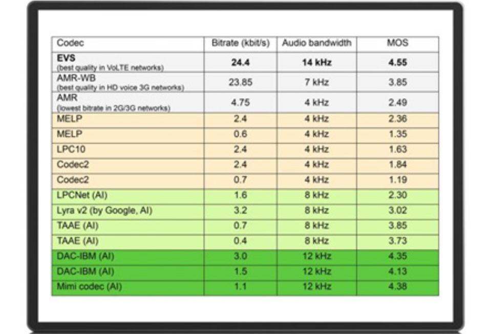
The detailed results of this evaluation, including statistical analysis, codec performance rankings, and listener feedback, are presented at the ITU-T SG12 meeting in September 2025. These insights are expected to contribute to ongoing discussions around codec standardisation, the definition of “quality,” and its automated prediction, particularly in the context of future mobile and satellite communication systems.
The post How good are ultra-low bitrate speech codecs? appeared first on ELE Times.
Photon Bridge and CPFC partner to validate path to scalable multi-wavelength light engines
NXP CoreRide Puts Automakers on Fast Path to 48 V Scalable Zonal Architectures
NXP Semiconductors introduced its NXP CoreRide Z248 zonal reference system – the semiconductor industry’s first pre-validated, design-ready zonal foundation that combines advanced 48 V energy distribution, deterministic data handling, functional safety, and real-time responsiveness. The hardware-software foundation is designed to optimise system performance, reduce system integration effort, shorten development cycles, and allow OEMs and Tier 1s to focus investment where it matters most. It sets a new benchmark for accelerating the journey from zonal architecture concepts to production‑ready implementations.
Built on NXP’s S32K5 microcontroller series, its integrated advanced MRAM technology unlocks ultra-fast, ultra-frequent over-the-air updates throughout the entire vehicle lifecycle. At the software level, the Z248 integrates a comprehensive pre-validated software stack that streamlines complex development of smart data energy network (SDEN) functionalities such as impedance, power and protection monitoring, intelligent data routing, AI‑enabled virtual sensing, diagnostics, and audio.
With its built-in, validated remote protocol stack (RCP), it supports the up-integration of end node functions and ECU consolidation to enable new cost-optimised vehicle architectures. It also addresses key challenges of 48 V zonal systems by managing energy conversion, distribution, and protection within a single, integrated architecture.
The Z248 is rigorously validated through thousands of system-level tests demonstrating outstanding low-power modes, fast boot and fast wake-up response. It is supported by a modern, collaborative continuous integration, continuous testing and continuous delivery (CI/CT/CD) development environment that allows significantly faster test loops with OEMs and tier 1s, shortening validation cycles.
Why it matters: Automakers are being asked to move faster, scale broader, and spend smarter – even as safe zonal consolidation, hybrid power systems, and AI-enabled features dramatically increase architecture complexity. NXP’s new CoreRide zonal reference system brings scalability to this rising architectural complexity. It reduces risk by helping OEMs and tier 1s accelerate development into production, and it eases the switch from legacy platforms and lower total cost of ownership – freeing them from complex integration to put them on a path to production.
“As new E/E architectures redefine vehicle design, our focus is simple: give the automotive ecosystem the foundation to move faster and differentiate with confidence,” said Sébastien Clamagirand, SVP and General Manager, Automotive Systems & Platforms at NXP Semiconductors. “The NXP CoreRide zonal reference system Z248 delivers a performance-optimised, scalable 48 V foundation that intelligently fuses power, data and software, while dramatically simplifying system integration, reducing time to market, and enabling OEMs to focus on vehicle differentiation and long‑term value creation.”
More details: The Z248 zonal reference system is delivered with a complete Board Support Package (BSP) with pre-integrated software from the NXP CoreRide partner ecosystem, including GLIWA’s performance monitoring suite, Green Hills’ software compiler and Vector’s embedded software and tools. The full package undergoes extensive validation to help ensure optimised performance, while continuously improving processing efficiency and power consumption based on the primary use cases of a zonal ECU.
It’s a scalable, safe and secure hardware-software stack that adapts easily to different variants of SDV E/E architectures and integrates naturally with NXP’s broader system offering. It leverages technologies across computing, networking, power management and 48 V energy distribution, including NXP’s S32K566 zonal microcontroller featuring on-chip MRAM that significantly accelerates ECU programming times, both in factory settings and during over-the-air (OTA) updates.
The reference system also integrates 48‑volt‑capable power components such as eFuse, PMIC and DC‑DC converters, robust in‑vehicle networking through Ethernet PHY and CAN transceivers, and built-in audio support. In addition, it introduces a new concept for zonal I/O extension. Designed for broad applicability with housing and a wiring loom, the new NXP CoreRide Z248 zonal reference system can be deployed across ICE, hybrid and BEV platforms, supporting the industry’s move toward zonal processing and ECU consolidation.
Ecosystem Voices
Peter Gliwa, CEO and Founder of GLIWA
“NXP understood that the eco-system, the tooling around a new platform, is essential for its success. With our Analysis Suite T1 built into the NXP CoreRide Z248 zonal reference system, high efficiency, proper timing analysis and timing verification are very well addressed.”
Dan Mender, Vice President of Business Development at Green Hills Software
“Green Hills is proud to play a central role in NXP’s transformative reference solution strategy, which simplifies and accelerates production-focused automotive ECU development through pre-integrated hardware and software optimised for zonal automotive architectures. By leveraging Green Hills’ integrated software solutions, customers can develop high-quality, safety-critical applications with a minimal footprint and optimal performance, while significantly reducing time to deployment.”
Sam Yeh, Chairman of Inventec
“In response to the automotive E/E architecture trend toward zonal and centralised designs, Inventec is collaborating with NXP Semiconductors to support the advancement of next-generation zonal architectures. Through this collaboration, Inventec can provide hardware design and JDM support to OEMs as part of NXP’s zonal E/E architecture initiatives.”
Jochen Rein, Senior Vice President, Business Unit Software Platform at Vector
“The combination of the NXP CoreRide platform and Vector’s software foundation provides a robust basis for next‑generation zonal architectures. We enable our joint customers to reduce their time- to-market due to a pre-integrated and highly optimised software stack.” Vector contributes as an NXP CoreRide partner, providing pre‑integrated software and tools that help streamline development and ensure smooth integration within the zonal ECU architecture.”
The post NXP CoreRide Puts Automakers on Fast Path to 48 V Scalable Zonal Architectures appeared first on ELE Times.
5 decade antilogarithmic PWM current source

The pages of Design Ideas (DIs) have recently been awash in a veritable cascade of designs for variable frequency oscillators with frequency ranges tunable over multiple decades:
- Self-oscillating sawtooth generator spans 5 decades of frequencies
- 555 VCO revisited
- 5 octave linear(ish)-in-pitch power VCO
- Tune 555 frequency over 4 decades
- Wide-range tunable RC Schmitt trigger oscillator
But despite the size of this crowd, a notable feature missing from all is provision for digital control (e.g., from an MCU GPIO pin) of the oscillation frequency. This DI will address that topic.
Wow the engineering world with your unique design: Design Ideas Submission Guide
When starting the design of any digital to analog interface, the first question to be answered is how much resolution (bits) do we need? For the applications listed above, the answer isn’t obvious. That’s because of the extremely wide range of the analog quantity (frequency) involved, e.g., 100,000:1 for Christopher Paul’s 5-decade 10 Hz to 1 MHz sawtooth generator.
5 decimal decades = 10ppm and is equivalent to a linear binary resolution of 16.6 bits. So even if we went with the overkill choice of 16bits (1/65536 = 15ppm), we’d still lose resolution at the bottom end. The first least significant bit (lsbit) increment up from 10 Hz would comprise a 15 ppm of 1 MHz = 15 Hz jump to 25 Hz, nearly trebling the output frequency.
Figure 1’s circuit takes an approach very different from linear conversion. Working from mere 8bit PWM, it makes lsbit incremental resolution constant and uniformly distributed at ~5% of output. Here’s how it works.
 Figure 1 Antilogarithmic 8-bit PWM gives s constant incremental ~5% per lsbit. Asterisked parts are 1% or better precision (metal film or C0G).
Antilog conversion occurs in a four step ~1ms cycle defined by the combined states of the GPIO PWM bit and D flip/flop decoded by the 4052 analog switch as shown in Figure 2.

Figure 2 Tw = antilog RtCt timeout = 1 to 250 counts = 2 to 500 µs, where
PWM = 1 + 21.63*Ln(Imax/Iout)
The antilog conversion sequence is as follows:
- BA = 3. duration 12 µs. Timing capacitor Ct charged to Vdd – 1.24 V.
- BA = 2. duration Tw = 2 µs to 500 µs. Ct exponentially discharged toward Vdd with time-constant RtCt = 43.4 µs.
- BA = 1: duration 0 to 498 µs. Ct residual charge transferred to Csh sample and hold cap.
- BA = 0: duration 2 µs to 500 µs. Ct residual charge continues to transfer to Csh.
At the end of each 4-step, 1024-µs cycle, Csh will converge toward a charge relative to Vdd between 12 µV and 1.2 V, determined by the antilog of the 2 µs to 500 µs duration of phase 2 of the conversion sequence. The 1-µV typical input offset of the LT2066 makes this adequate for (reasonably) accurate digital to analog conversion. Convergence of Vcsh to 8-bit precision takes a maximum of 8 cycles = 8.2 ms.
Final conversion of the resulting 5-decade current source to a 5-decade frequency output (the point of the exercise) can be done simply (if admittedly kind of crudely) with the circuit in Figure 3.

Figure 3 A minimal 5-decade sawtooth oscillator that enables final conversion of the resulting 5-decade current source to a 5-decade frequency output.
Or it can be done much more precisely with Christopher Paul’s DI by substituting Figure 1 for his original resistor-programmed current source (highlighted in yellow), as shown in Figure 4.

Figure 4 Maximal 5-decade sawtooth oscillator, using Christopher Paul’s DI.

Figure 5 Log (red) and linear (black) plot of source current versus PWM.
Stephen Woodward‘s relationship with EDN’s DI column goes back quite a long way. Over 200 submissions have been accepted since his first contribution back in 1974. They have included best Design Idea of the year in 1974 and 2001.
Related Content
- Self-oscillating sawtooth generator spans 5 decades of frequencies
- 555 VCO revisited
- 5 octave linear(ish)-in-pitch power VCO
- Tune 555 frequency over 4 decades
- Wide-range tunable RC Schmitt trigger oscillator
The post 5 decade antilogarithmic PWM current source appeared first on EDN.
Microchip Helps Manufacturers Meet Cybersecurity Regulations, Expands Security Services in the Trust Platform
The post Microchip Helps Manufacturers Meet Cybersecurity Regulations, Expands Security Services in the Trust Platform appeared first on ELE Times.
Sivers to supply lasers and optical amplifiers worth $53–138m over customer’s product life-cycle
POET demos hybrid laser and next-gen high-power external light source for AI at OFC
Fuel cell sensors: From breath to benchmark

Fuel cell sensors are electrochemical devices designed for precise measurement. In measurement applications, they have become the gold standard for breath alcohol concentration detection, valued for their ethanol specificity, stability, and courtroom-grade accuracy. Compact and low power, they form the backbone of law enforcement breathalyzers, workplace safety programs, and consumer devices, consistently outperforming semiconductor and infrared (IR) alternatives.
Their proven reliability in complex breath matrices has made them indispensable for safety and compliance, while ongoing innovation is extending their reach into broader analytical domains. And while fuel cells generate clean energy, fuel cell sensors generate precise measurements—a distinction that defines their unique role in modern technology.
Applications and history
Before we get into the basics of how fuel cell sensors work, it’s worth noting their application landscape. While research has explored microbial fuel cell biosensors for environmental monitoring and niche industrial uses, the overwhelming commercial reality today is breath alcohol concentration (BAC) measurement.
Fuel cell sensors have become synonymous with BAC detection because of their unmatched ethanol specificity, stability, and courtroom-grade accuracy. Although BAC formally refers to blood alcohol concentration, in practice it is estimated through breath alcohol analysis. This singular focus has defined their role in law enforcement, workplace safety, and consumer devices, making BAC not just their flagship application but essentially their identity in the marketplace.
Technology itself traces its roots to the 1960s, when early electrochemical cells were adapted to detect ethanol in breath samples. By the late 1970s and early 1980s, law enforcement agencies began adopting fuel cell-based breathalyzers, recognizing their superior specificity compared to semiconductor sensors.
Over time, improvements in miniaturization, catalyst stability, and calibration protocols transformed them from bulky instruments into compact, portable devices. This evolution cemented fuel cell sensors as the trusted backbone of alcohol detection, setting the stage for their enduring role in safety and compliance.

Figure 1 A compact breathalyzer with a fuel cell breath alcohol sensor—Alcotest 4000—simplifies portable BAC measurement. Source: Dräger
As a quick aside, while fuel cells rely on chemical reactions, IR spectroscopy uses light to identify alcohol’s unique spectral fingerprint. By directing an IR beam through a breath sample, the instrument measures the specific wavelengths absorbed by ethanol molecules.
This physics-based method is non-destructive and highly precise, enabling real-time detection of “mouth alcohol” that could otherwise distort results. Because of their sophistication, accuracy, and long-term stability, IR units are reserved as definitive, desktop-based instruments in police stations, providing the courtroom-grade evidence required for testimony.
Fuel cell breath alcohol sensors
Now is the time for a gentle dive into a bit of theory and practice. At their core, these sensors operate on an electrochemical principle: ethanol molecules in exhaled breath are oxidized at a platinum electrode, producing an electrical current directly proportional to concentration. This reaction is simple yet elegant, converting chemical energy into a measurable signal that reflects blood alcohol concentration (BAC).
In practice, this design delivers a combination of portability, stability, and specificity that has made fuel cell sensors the dominant choice for breath alcohol testing. Unlike semiconductor sensors, which can be affected by other volatile compounds, fuel cells respond almost exclusively to ethanol.
Their compact form factor allows integration into handheld devices, while their long-term consistency ensures reliable results in roadside, workplace, and consumer contexts. This balance of theory and application explains why fuel cell sensors remain the benchmark technology for BAC measurement today.
In a nutshell, a fuel cell breath alcohol sensor is essentially a pair of platinum electrodes immersed in a dilute acid electrolyte. When a trace amount of ethanol from exhaled breath reaches the electrodes, it undergoes oxidation, releasing electrons that flow as current. The magnitude of this current is directly proportional to ethanol concentration, providing a simple yet highly reliable way to quantify blood alcohol concentration.
And fundamentally, the fuel cell breath alcohol sensor consists of a porous, chemically inert layer coated on both sides with finely divided platinum black. The porous layer is impregnated with an acidic electrolyte solution, and platinum wire connections are attached to the platinum black surfaces. The assembly is mounted in a plastic case with a gas inlet for introducing a breath sample. While manufacturers add proprietary refinements to this design, the basic configuration is shown in Figure 2.

Figure 2 Drawing illustrates the basic construction of a fuel cell breath alcohol sensor. Source: Author
Hands-on with fuel cell alcohol detection
For those eager to explore fuel cell alcohol sensors, the FS00702 electrochemical ethanol content module offers a robust solution. This fuel cell–type sensor operates through oxidation and reduction reactions at the working and counter electrodes, generating charges that form a measurable current. Current’s magnitude is directly proportional to alcohol concentration, in accordance with Faraday’s law, enabling accurate determination of ethanol levels.
Equipped with a high-stability gas sensor and a high-performance microprocessor, the module supports both UART and analog signal outputs for seamless integration. Its precise automatic calibration and advanced detection systems minimize human interference, ensuring consistent accuracy and reliability in large-scale production environments.

Figure 3 Highlighting FS00702 key specs: enabling makers to detect ethanol with precision, rapid updates, and easy microcontroller integration. Source: Henan Fosen Electronics Technology
As a side note worth mentioning, ethanol is one specific type of alcohol—the compound found in beverages and fuels—whereas “alcohol” broadly refers to a family of related molecules such as methanol, propanol, and isopropanol.
Fuel cell sensors like FS00702 are calibrated for ethanol detection since it’s the relevant analyte for intoxication measurement and fuel monitoring. While the sensor may respond to other alcohols, its accuracy is optimized for ethanol, making precise terminology important in technical contexts.
Practically speaking, sourcing high-quality fuel cell alcohol sensors for hobbyist projects is challenging, since most manufacturers prioritize finished breathalyzer units or bulk industrial modules.
Still, there are accessible alternatives to FS00702 for makers who value the accuracy and specificity of fuel cell technology. The Dart Sensors 2-Electrode fuel cell is considered a gold standard for precision, though it requires a custom amplifier circuit.
Fosensor’s FS00701 provides a smaller footprint than FS00702, ideal for portable builds. Meanwhile, FS00702 itself remains versatile, offering both raw analog output for custom conditioning and a built-in UART option for straightforward microcontroller integration.
Winsen’s ZE321 automotive alcohol module offers a compact design with a convenient UART interface, making it more user-friendly for DIY integration. The ZE321 module operates on the fuel cell electrochemical principle. When the built-in pressure sensor detects exhaled air flowing through the sampling tube at the required rate, the solenoid valve quickly opens to admit a measured volume of breath.
Within the sensor, alcohol and oxygen undergo a redox reaction, generating an electrical current proportional to ethanol concentration. The module’s circuitry measures this current and, after algorithmic processing, outputs an accurate determination of breath alcohol content.

Figure 4 The ZE321 automotive alcohol module monitors exhaled breath flow, samples a fixed volume of gas, and actively detects alcohol content through its fuel cell electrochemical reaction. The onboard circuitry processes the resulting current signal to deliver accurate breath alcohol measurements. Source: Winsen
Accuracy today, innovation ahead
In practical terms, fuel cell–based alcohol testing devices deliver the highest accuracy in measuring breath alcohol content, leaving little room for error. Even so, it’s wise to allow for a small margin of discrepancy. When evaluating any alcohol detection instrument—whether for personal safety, workplace compliance, or automotive use—the sensor type is critical. If precision matters most, fuel cell sensor technology remains the benchmark to aim for.
For makers and engineers, the challenge is clear: fuel cell sensors are not confined to alcohol testing; they are gateways to precision sensing, sustainable energy, and inventive applications across domains. Experiment boldly, share your builds, and push the boundaries of what these devices can achieve. The next breakthrough could start on your workbench.
 T. K. Hareendran is a self-taught electronics enthusiast with a strong passion for innovative circuit design and hands-on technology. He develops both experimental and practical electronic projects, documenting and sharing his work to support fellow tinkerers and learners. Beyond the workbench, he dedicates time to technical writing and hardware evaluations to contribute meaningfully to the maker community.
Related Content
- Hydrogen Fuel-Cell Vehicles
- Paper-Based Biofuel Cells Power Disposable Electronics
- xEVs Opening New Opportunities for Sensor Development
- Designing a portable system for in situ failure prediction in fuel cells
The post Fuel cell sensors: From breath to benchmark appeared first on EDN.
Everspin Launches New Generation of Unified Memory for Embedded Systems
Everspin Technologies, a leading developer and manufacturer of magnetoresistive random access memory (MRAM) persistent memory solutions, today announced the UNISYST MRAM family, a new generation of unified memory designed to fundamentally change how embedded systems store and access code and data.
“System designers are running into the physical and performance limits of NOR flash, especially as process nodes move below 40 nanometers and workloads become more demanding,” said Sanjeev Aggarwal, president and CEO of Everspin Technologies. “With UNISYST, we are extending our MRAM roadmap to higher densities while giving customers a practical way to start with PERSYST today and migrate to a code-and-data MRAM architecture as soon as it is available.”
UNISYST is a unified code-and-data MRAM architecture that bridges traditional configuration memory and higher-density persistent storage, extending MRAM into traditional NOR flash applications where superior performance, endurance and reliability are valued. Built as a natural extension of Everspin’s existing PERSYST MRAM platform, UNISYST gives customers a practical, simple migration path from today’s serial MRAM devices to higher-density unified memory without requiring changes to system architecture or software.
Everspin will initially offer the UNISYST family in densities ranging from 128 megabits to 2 gigabits, using a standard xSPI interface operating up to octal SPI at 200MHz. The devices are planned to feature AEC-Q100 Grade 1 qualification and minimum 10-year data retention at extreme temperatures, supporting demanding environments across automotive, aerospace, industrial and edge AI applications.
“As generative AI models move from the cloud to embedded systems, we’re suddenly dealing with assets that are tens or even hundreds of megabytes in size,” said Kwabena W. Agyeman, President and Co-founder of OpenMV. “Storing those models is only part of the challenge — updating them quickly during development and deployment is equally important. High-speed, non-volatile Everspin UNISYST MRAM changes what’s practical for edge AI systems by removing the write bottlenecks associated with traditional flash.”
UNISYST delivers high-bandwidth read and write speeds in a non-volatile memory device, enabling fast boot, rapid updates and predictable performance without the tradeoffs of traditional flash-based designs. By combining high-speed access with persistent storage, UNISYST supports software-defined systems that require frequent reconfiguration while maintaining data integrity across power cycles.
Everspin MRAM has been deployed in mission-critical storage applications for nearly two decades, valued for its endurance and reliability. UNISYST builds on Everspin’s proven MRAM foundation with capabilities designed to support more complex, software-defined systems:
- Code-and-data MRAM architecture designed as a next-generation alternative to other non-volatile memory
- Standard xSPI interface operating up to octal SPI at 200MHz
- Read bandwidth of up to 400 MB/s and write bandwidth of approximately 90 MB/s, over 400 times faster than NOR flash
- Write endurance up to 10 times higher than typical NOR
- AEC-Q100 Grade 1 qualification and minimum 10-year data retention for high-reliability designs
UNISYST is aimed at applications where non-volatile memory must combine high bandwidth, high endurance and predictable behaviour over temperature and time. Target use cases include:
- AI at the edge: Fast AI weight updates, critical storage at the edge, local code-and-data storage for workloads that need fast boot, rapid reconfiguration and non-volatile operation close to the sensor, with the ability to execute in place, removing the need for multiple system memories
- Military and aerospace: Field-programmable gate array (FPGA) configuration and code storage for mission-critical systems, including low-Earth orbit satellites and other platforms that require frequent over-the-air updates
- Automotive: Control, logging and configuration memory in systems that must meet Grade 1 temperature requirements and long-term data retention
- Industrial and casino gaming: High-traffic logging and configuration in environments that demand fast writes, long endurance and persistent storage supporting data logging
The launch of UNISYST represents a platform-level expansion of Everspin’s MRAM portfolio, extending the company’s role from a niche memory supplier to a mainstream memory player serving a multibillion-dollar market. By unifying code storage and data memory, Everspin is addressing the growing demands of software-defined systems that require faster boot times, frequent updates and predictable behaviour over long operating lifetimes.
The post Everspin Launches New Generation of Unified Memory for Embedded Systems appeared first on ELE Times.
Photon Design showcasing new HAROLD QD laser simulator and silicon modulator design tool at OFC
Сторінки


![[link]](https://i.redd.it/p67zykun3iog1.jpeg)